Plasmonic Nano-Gap Tilings: Light-Concentrating Surfaces for Low-Loss Photonic Integration
Abstract
Owing to their ability to concentrate light on nanometer scales, plasmonic surface structures are ideally suited for on-chip functionalization with nonlinear or gain materials. However, achieving a high effective quantum yield across a surface not only requires strong light localization but also control over losses. Here, we report on a particular class of tunable low-loss metasurfaces featuring dense arrangements of nanometer sized focal points on a photonic chip with an underlying waveguide channel. Guided within the plane, the photonic wave evanescently couples to the nano-gaps, concentrating light in a lattice of hot-spots. In studying the energy transfer between photonic and plasmonic channels of single trimer molecules and triangular nano-gap tilings in dependence on element size, we identify different regimes of operation. We show that the product of field enhancement, propagation length and element size is close-to-constant in both the radiative and subwavelength regimes, opening pathways for device designs that combine high field enhancements with large propagation lengths.
-
Nano-gap tiling, Low-loss plasmonics, Silicon photonics, Waveguide integration, Mode hybridization
![[Uncaptioned image]](/html/1305.2839/assets/x1.png)
Mediated by subwavelength interactions with metallic particles, nanoplasmonic surfaces can alter the localization and propagation characteristics of light at interfaces.1, 2, 3 The steady progress in lithographic4, 5 and self-assembly techniques6, 7 makes it possible to shape metallic surface elements with increasing precision, reaching towards sub-nm scales.8 In the wake of this technological development, schemes involving coupled plasmonic particle clusters and arrays have been designed, fabricated and studied, exploring their potential to slow or stop light, 9, 10, 11 to nano-focus light in the gaps between or at the edges of the nano-particles,12, 13 to resonantly transport energy along particle chains,14 to control the phase,15, 16, 17 polarization16, 18 and to refract light at negative angles.15, 17
As research continues to explore nanoplasmonic surfaces with engineered optical properties and their functionalization with nonlinear and quantum gain 19, 20 materials as diverse as gases 21, semiconductors22, dyes 23 and graphene24 there is a growing gap between the wealth of potential applications and practical concepts for on-chip integration with photonic technologies. In fact, until now, plasmonic and metamaterial surfaces are mostly operated out-of-plane; i.e. by illumination under normal incidence or evanescent excitation with near-field microscope tips;25, 26, 27 two well-established techniques that are convenient to perform, yet with limited potential for on-chip integration. Fundamentally, integration with photonic circuitry requires keeping light confined and in interaction with the structured surface, without inducing uncontrolled scattering or excessive dissipative loss. The usual trade-off is that a stronger confinement of light to the metallic surface increases attenuation and heat generation due to Ohmic losses.28, 29, 30 Hybrid metal-dielectric waveguide structures 31, 32, 33, 34 offer one possibility to break the interdependency of loss and localization, but require careful design to achieve good loss-performance and compatibility with established photonic architectures. Furthermore, from a fabrication and integration perspective, it is highly desirable to establish a platform where light waves, guided within a photonic layer, can be manipulated on subwavelength scales using metallic nano-structures on the surface.35 Such hybrid platforms may not only provide well-defined interfaces for on-chip integration of plasmonic devices (e.g. sensors or spectroscopic elements) with photonic signal-processing circuits, but also offer practical routes towards active nanoplasmonic components that exploit the enhanced surface-interaction with fluorescent,36 magneto-optic37 or nonlinear materials.21
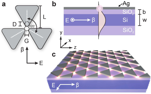
In this article we report on a particular class of integrated plasmonic surface structures, plasmonic nano-gap tilings (NGTs), featuring dense lattices of focal points (1). To understand the general properties of plasmonic NGTs, we theoretically study one of the simplest structures: triangular surface patches of fixed orientation arranged in a triangular lattice. The chosen combination of shape and lattice was guided by our aim to concentrate light in a dense array of hot-spots to achieve a strong enhancement of the surface fields.
The surface structure is fully characterized by the pitch , given by the projection of lattice vectors and in the propagation direction, the gap and the element corner rounding of diameter (1a). The triangular NGTs borrow symmetry and light-enhancing properties from the trimer molecule. As shown in 1(a) both the symmetry of the molecule and two sets of directional axes of excitation ( and ) are retained in the assembled 2D tiling (1c).
We consider thick silver () structures on top of a planar dielectric stack consisting of silicon oxide () substrate, a planar thick silicon () waveguide, and a buffer layer of tunable thickness (1b). To maintain the lateral mode profile, we operate at a fixed wavelength of where the guiding layer supports only the fundamental transverse electric (TE) and magnetic (TM) modes. At this wavelength the complex permittivity of the silver38 can be approximated by .
RESULTS AND DISCUSSION
Waveguide Integration.
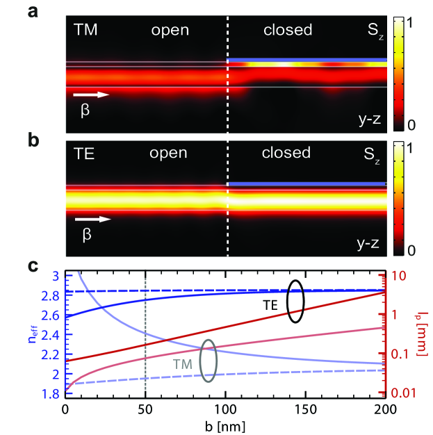
To characterize the fundamental properties of the hybrid platform, we first study modes impinging on the interface between the open (i.e. uncovered) and closed (i.e. metal covered) waveguide sections. For TM polarization (2a), the mode hybridizes33 with the surface plasmon polariton (SPP) mode at the metal-buffer interface, concentrating the energy in the low index buffer.39, 40, 41 As a consequence, both the mode profiles and the effective refractive index (2c; light blue lines) between the two sections mismatch strongly; in particular for . In contrast, the TE mode (2b) retains its photonic character across the discontinuity and, while being slightly pushed down into the low-index substrate, experiences a considerably smaller perturbation of its profile and a change in its effective index (2c; dark blue lines). More specifically, at , the effective refractive index mismatch, , between the open and closed sections for a TE excitation amounts to , compared to in the TM case. We also note that the propagation length of the TE mode is consistently larger than that of the TM mode and rises strictly exponential with increasing buffer height (2c; red lines, right axis). This exponential behavior at small buffer heights indicates that, for TE excitation, losses are induced by the evanescent tail of the mode profile touching the metallic surface rather than the direct coupling in the case of the TM mode. At , we record a value of ; roughly twice as high as the corresponding TM value confirming that the TE mode not only features the better matched mode profile, but is also more favorable in terms of dissipative loss.
Trimer Surface Antenna: Scattering Spectra.
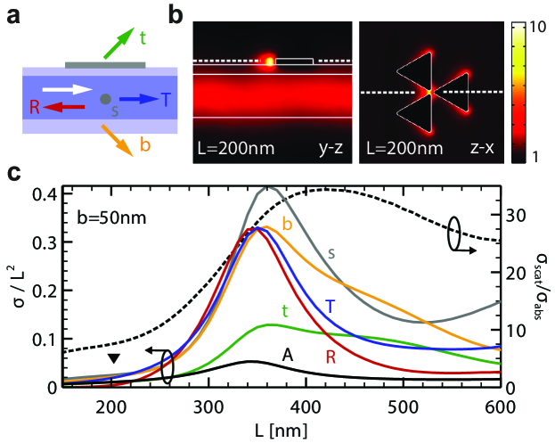
Field concentration in the focal points is achieved via evanescent interaction of the guided TE mode with surface elements. To explore this mechanism we first consider an isolated trimer molecule42 (1a) of individual element size . The isolated trimer can be understood as a plasmonic surface antenna that is evanescently driven by the photonic field, absorbing and scattering energy into the various in- and out-of-plane channels (3a). 3c shows the scattering and absorption cross-sections associated with the different channels. The ratio of scattered energy to the absorbed energy (dashed line, right axis) shows that the absorption is times lower than scattering, as the antenna cannot be considered small compared to the effective wavelength of . For , in the subwavelength regime, the scattering cross-sections are smaller than . With increasing , the various scattering cross-sections (left axis) rise and peak at , due to the excitation of localized surface plasmon resonances (LSPRs). Owing to the strong refractive index mismatch between the air cladding and silicon waveguide, the top scattering is weakest while the scattering to the side achieves the highest cross-section of just above . Beyond the dipolar resonance the scattering cross-sections drop, except those related to the out-of-plane scattering (channels and ) that exhibit a characteristic shoulder. This suggests the presence of another radiative resonance at around . The exceptional stability of the driving photonic field, even at resonance, is one of the characteristics of TE excitation that makes this configuration inherently suitable for the optically driven chip-integrated plasmonic antennas.
Trimer Surface Antenna: Field Enhancement.
Despite the weaker evanescent surface interaction, the TE-polarized photonic field can lead to strong lateral charge separation within the metallic surface elements. This can lead to capacitive coupling in the nano-gaps between the elements inducing strong fields which peak at resonance.43, 44As shown in 3b, the field concentrates on the surface into bright spots at the corners of the antenna, while the propagating field in the waveguide below remains mostly unperturbed.
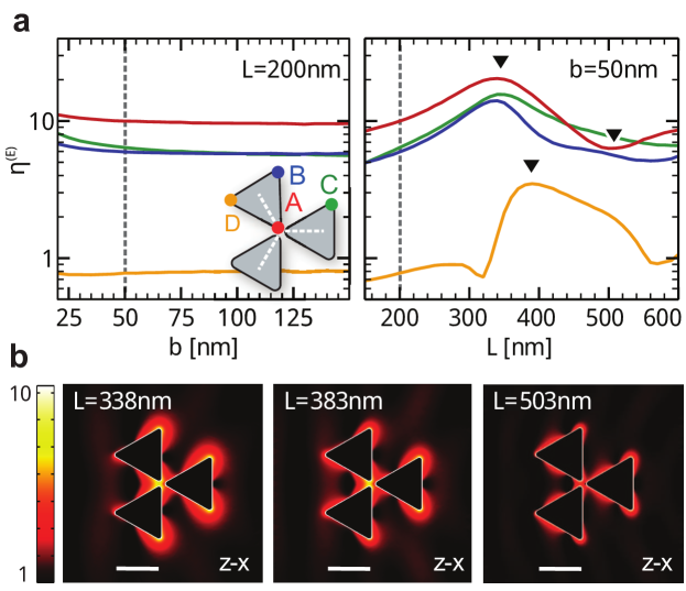
To quantify the achieved light concentration, we measure the relative surface enhancement, , of the electric field at the different corners of the trimer (4a; inset) by dividing the field amplitude averaged over a small volume around the respective corner by the same surface field without the antenna, i.e. (). The results in 4 give a strong indication that the spot-enhancements are largely independent of buffer height (4a; left panel), as the evanescent surface field is effectively funneled into the central focus point without a significant perturbation of the mode propagating within the waveguide. With increasing size , the antenna (4a; right panel) becomes resonant (at ) and the field enhancement at the center position increases from to . The position of the enhancement peaks (and dips) depends critically on the position of evaluation. The most distinct features are the peaks of , and at around , the broad peak of at , and the dip of at around (see markers in 4a). 4b shows the two resonant states of the antenna, characterized by a strong lateral charge separation (; left panel) and an additional longitudinal charge separation (; middle panel). With increasing size additional nodal planes in the longitudinal direction become visible (; right panel) as a signature of wave retardation. As the element size becomes comparable to the effective wavelength of the waveguide mode, the polarizing electric field changes orientation across the antenna, exciting higher order (subradiant) modes. This retardation effect also illuminates the otherwise dark corner and causes, in weakening the lateral resonance, a decrease of the enhancement in the center.
Nano-Gap Tiling: Scattering Spectra.
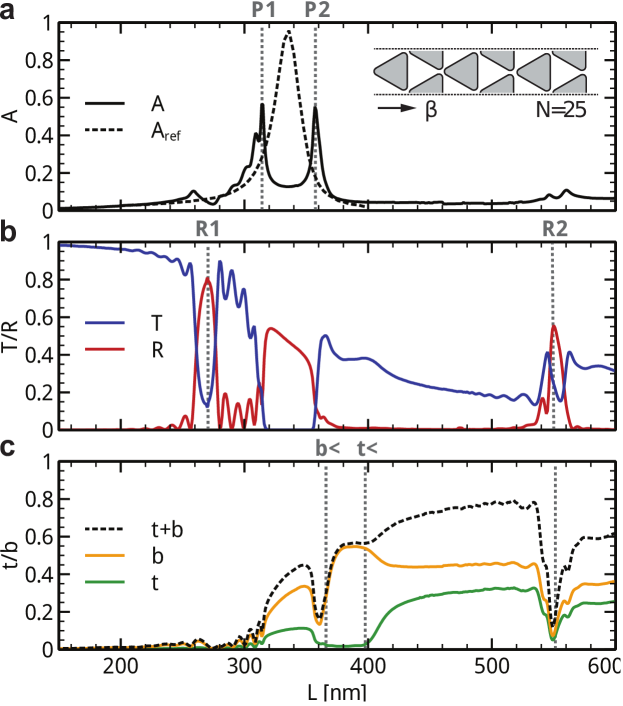
Having established how light is focused and scattered by a single trimer molecule on the surface, we proceed to study the optical characteristics of triangular nano-gap tiling (NGTs), which can be understood as a dense array of coupled trimer molecules. These structures are of particular practical interest as they allow for in-plane excitation of a dense array of bright spots accessible from the surface. For the following we chose a laterally periodic array of triangular elements in propagation direction. To gain an understanding of the photonic and plasmonic resonances of integrated NGTs, we first compare the change of absorption of the triangular NGTs for out-of-plane excitation (via total internal reflection) and in-plane excitation (from the waveguide) with varying element pitch .
5a (solid black line) shows the calculated absorption spectrum for in-plane excitation for buffer and waveguide heights of and , respectively. The absorption spectrum shows two distinct peaks, marking, as can be seen from the spectra in 5b, the edges of a transmission stop-band. To understand the origin of the hybridization in the waveguide-integrated configuration, we compare the in-plane absorption spectrum with the absorption of the NGT under out-of-plane excitation. We place the NGT on a thick buffer of thereby isolating the NGT from the influence of the silicon layer. To recreate the same conditions of excitation as for in-plane excitation we inject a plane wave from a semi-infinite substrate (prism) below the buffer at an incident angle of . At this angle the injected plane wave experiences total internal reflection at the / interface and can only evanescently couple to the surface tiling with an in-plane projection of the wave vector that precisely matches the propagation constant of the waveguide mode. The result, plotted as dashed line in 5a, shows a single broad plasmonic resonance at around centered between the two in-plane absorption peaks. The splitting of the plasmonic resonance and the emergence of a transmission stop-band is a result of the interaction between the plasmonic resonances of the tiling with the propagating mode in the waveguide. When the trimer molecules are coupled in a dense array, the LSPRs couple to a plasmonic band that supports propagation of SPPs along the chain of nanoparticles.14 The mutual coupling of the propagating plasmonic and photonic modes leads to the formation of waveguide-plasmon polaritons, which, due to the strong coupling (low buffer height), anti-cross at the point where the frequencies and -vectors of the plasmonic and waveguide modes match.45 As a consequence of the mode hybridization, the observed mode-splitting increases with decreasing buffer size as the coupling parameter between the waveguide and the surface plasmonic modes become exponentially stronger.
A fundamental difference between in-plane and out-of-plane excitation concerns the number of available scattering channels. While plane-wave ATR spectroscopy measurements record energy transfer into absorption (A), transmission (T) and reflection (R) channels, one must, for integrated designs, also consider the scattering into the superstrate (t; top) and the substrate (b; bottom). In 5b/c we show the scattering coefficients of the triangular NGT over in the range to . With the structure becoming resonant to the effective wavelength (), it acts as a plasmonic crystal.46, 47, 48 Both plasmonic and photonic scattering are mediated by the triangular lattice of the NGT. In the propagation direction, the projection of the incident wave vector (the propagation constant ) on the reciprocal lattice vectors ( and ) are equal. The -matching condition dictates that the in-plane projection of the scattered wave vector equals the incident wave vector plus multiples of the effective lattice vector . Using we associate with the scattering angle relative to the surface-normal and the refractive index of the scattering channel. Resolving this condition with respect to gives
| (1) |
Apart from the plasmonic stop-band between and (5a), there are two more stop-gaps (at and ) in the spectrum (see 5b), which can be explained by resonant back-scattering. Setting and in (1) gives , the Bragg conditions for the first and second () order reflection peaks at and , which are in excellent agreement with 5b. In contrast, out-of-plane scattering into the substrate () and air () can occur over the whole lower and upper half-space. Again using equation (1), we mark the points for as and for scattering to the top and bottom respectively. We also note that the second Bragg peak at always coincides with normal-to-plane scattering into the substrate and superstrate, reducing the proportion of energy transmitted into these channels.
Nano-Gap Tiling: Surface Field Enhancement.
Changing the pitch of the NGT does not only affect the scattering of energy into the various channels but has a strong impact on the concentration of energy on the surface as the plasmonic resonance and localization of fields in the waveguide changes. To investigate the enhancement of fields we (as before) inject a waveguide mode into a NGT with elements and record the laterally (along -direction) averaged intensities on the surface and in the center of the waveguide . To obtain the relative field intensities on the surface and inside the waveguide, we divide by and , the bare intensities without the NGT on the surface (6; left panels). Finally, to quantify the net enhancement of the field we average the normalized intensities on the surface and inside the waveguide along the propagation direction (6; right panels). The results show that the normalized surface intensities peak at the hybrid resonances at and . Both the plasmonic stop gap and the Bragg resonances inhibit propagation in the waveguide, leading to strong attenuation of the fields in the propagation direction. However, owing to the excitation of SPPs, energy keeps propagating in form of SPPs on the surface with less attenuation, leading to an elevated surface field enhancement in these spectral regimes (compare 6a and 6b).
For pitch lengths above the plasmonic resonances the surface intensities weaken due to the onset of out-of-plane scattering. In contrast, below the first Bragg resonance, in the subwavelength regime, the strength of the surface intensities settles at an average value of , while the average intensity in the waveguide remains across the length of the NGT. This off-resonant enhancement of surface intensities can be attributed to the lightning rod effect,49 which leads to a concentration of field strength into the focal points of the NGT without inducing high plasmonic losses.
For functionalization of the surface (e.g. with polymers, dyes, etc.) we are interested in the effective enhancements of the linear and nonlinear susceptibilities of the material deposited. To find the enhancement for a particular process, we divide the ’th power of the normalized surface field by the normalized electric field within the waveguide and integrate over the area of the NGT. For example the effective intensity enhancement () is given by
| (2) |
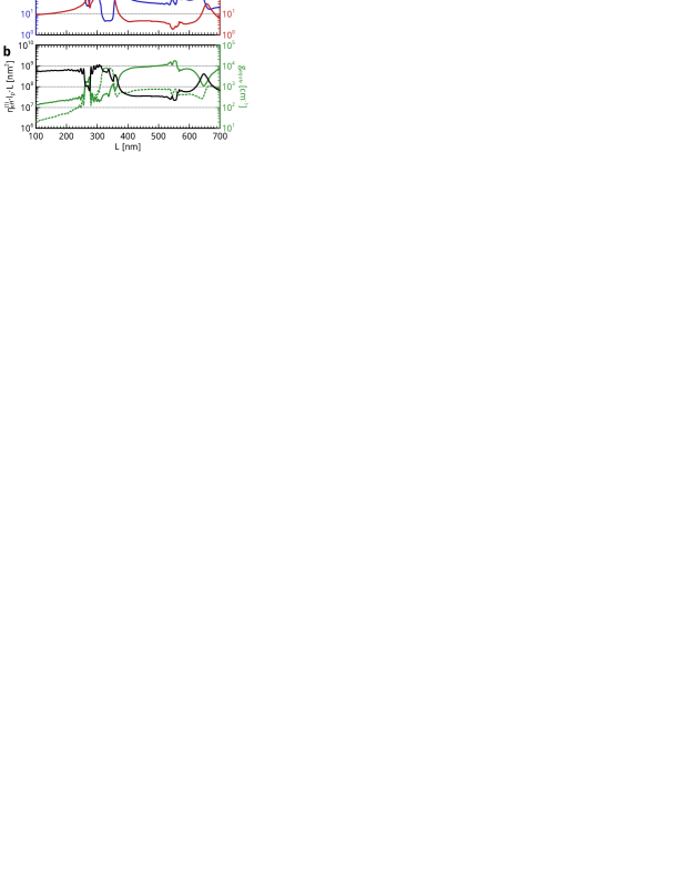
The fact that we divide the surface intensities at every point by the intensity in the waveguide underneath allows us to eliminate propagation effects such as attenuation, back-reflection and standing wave patterns. This approach is valid as the evanescent interaction of the waveguide fields with the surface structure does not involve significant retardation effects. The so-obtained effective enhancement of the surface intensity is plotted in 7a (red line) together with the unit-less effective propagation length (blue line) over the pitch . One notices that, in the off-resonant regime, the per element propagation length decreases exponentially for decreasing pitch values, while the effective enhancement of the surface intensity asymptotically approaches a value of . When the pitch approaches the plasmonic resonance of the NGT at around , the effective propagation length is at a minimum as the plasmonic stop gap prevents propagation of the wave. The effective intensity enhancement is strongest in this regime as the NGT is excited resonantly, leading to high field concentrations (relative to the waveguide fields) in the gaps that propagate in form of SPPs along the surface. For pitch values larger than , where out-of-plane scattering dominates, the values of and change only slightly with the pitch.
Nano-gap Tiling: Equivalent Gain.
Although the achieved intensity enhancement in the subwavelength regime is comparably low, the propagating photonic field experiences low attenuation and remains in interaction with the NGT. To quantify the trade-off between field concentration and attenuation we introduce an effective attenuation cross-section
| (3) |
which is shown in 7b (black line). Strikingly, this cross-section is close-to-constant in the subwavelength regime (below ) and in the radiative regime before the second Bragg resonance (). In these regimes
| (4) |
which means that the ability of the NGT to concentrate energy on the surface is proportional to the density of hot-spots () and the normalized attenuation (). This relation is of particular relevance in the context of device functionalization with nonlinear50 and gain materials.51, 52, 53 As an application, we imagine an active material deposited on the surface. To fully compensate the dissipative and radiative losses we require an equivalent gain of
| (5) |
introducing the confinement factor
| (6) |
which quantifies the proportion of energy that interacts with the gain region ( in the gain-filled section and 0 elsewhere). For the given structure we find that for a layer of gain media deposited on the buffer, in between the elements of the plasmonic NGT. The retrieved equivalent gain values are plotted as green line in 7b. In the subwavelength regime where the attenuation cross-section reaches a value of there is a linear increase of the equivalent gain with from at to at . At the first Bragg resonance () the gain values peak at before they drop again to values of only in the plasmonic stop gap, where the propagation constant is lowest but the effective enhancement highest (see 7a). Beyond the plasmonic resonances, radiative loss dominates and the field enhancement is low. This leads to high equivalent gain values of that would be required to compensate attenuation losses. The results illustrate that loss-compensation in the proposed hybrid structure is a realistic prospect even in the resonant plasmonic regime. Finally, we note that using epitaxially grown InGaAsP based semiconductors structures gain can also be introduced directly into the waveguide structure. In this case (keeping the geometric dimensions) the confinement factor is but there is no plasmonic field enhancement, resulting in the dashed green line in 7b. While the required gain for loss-compensation is generally lower, this is particularly not true in the regime where the waveguide mode couples to the surface plasmon resonances of the surface.
CONCLUSION
In conclusion we reported on a new class of low-loss integrated surface structures, plasmonic nano-gap tilings (NGTs), which can concentrate light on the surface of a photonic chip in a lattice of bright-spots. To understand their unique properties, we investigated triangular trimers in an integrated configuration, showing their potential to scatter and concentrate light on the surface of the chip in dependence of their size. For the assembled NGT we identified different regimes of operation depending on the pitch length: the off-resonant regime, where the NGT acts as true light-concentrating metasurface, and regimes dominated by in-plane (back) scattering, excitation of plasmonic modes, and out-coupling of radiation. Using a novel technique for the extraction of the field enhancement, we were able to define an effective attenuation cross-section, which plateaus in the off-resonant and radiative regime. The equivalent gain required for loss-compensation on the surface and in the waveguide illustrate that loss-compensation in these structures is realistically possible. The triangular structure that forms the basis of this work is one of many possibilities to cover a surface with a regular 2D tiling. The chosen combination of particle shape (triangles) and crystal lattice (hexagonal) was guided by our aim to concentrate light in a dense array of hot-spots on the surface. Tilings with higher symmetry, such as a checkerboard tiling (diamonds on a square lattice), are possible but do not achieve the same surface field enhancement, as, for a given propagation direction, only half of the nano-gaps are excited. We note that waveguide-integrated plasmonic surface arrays are not limited to the passive SOI platform, but can be also be integrated on active semiconductor material systems (e.g. III-V semiconductors). While surface functionalization with gain materials were considered in this work, other nonlinear materials can be conveniently deployed on the surface. The observed hybrid waveguide plasmon-polariton resonances are also highly sensitive to changes in the dielectric constant54 and could be employed for waveguide-integrated dielectric sensing applications that would additionally benefit from the field enhancement on the surface. In combining the low-loss, light-enhancing and resonant properties of plasmonic and photonic structures with NGT structures may offer new routes to hybrid devices, such as on-chip sensors, plasmonic couplers, active surface emitters, switches and all-optical modulators.
METHODS
Numerical Simulations.
All numerical simulations were performed in frequency domain using the full-vectorial finite-element method. To calculate the spectras of the isolated trimer elements we carried out scattering simulations with COMSOL using a two-step process: First we solved for the background field of the waveguide without the antenna using a combination of port boundary conditions (at the front and back) for waveguide mode injection, perfect electric boundary conditions (on the left and right) and perfectly matched layers (PMLs) on top and bottom. The calculation of the background field was followed by scattered-field calculations where the antenna was placed onto the waveguide. For this second step the PEC and PML boundaries have been replaced by PMLs enabling outward propagation of the scattered fields in all directions to determine the scattered energy flux. For the simulation of the finite NGT, we performed single step simulations using JCMwave. Periodic boundary conditions (PBC) were used for the sides of the structure to simulate a laterally infinite tiling. PMLs were used for the continuation of the sub- and superstrate layers, and the continuation of the forward and backward waveguide stack . The distance of the PMLs was chosen sufficiently large to avoid spurious backreflections and to accurately resolve the out-of-plane energy flow and the in-plane transmission and reflection coefficients.
The simulations were carried out for perfectly periodic structures and for a fixed direction of excitation by injection of a TE waveguide mode along the -axis. To investigate off-axis propagation and the impact of imperfections, such as spatially varying gap sizes or corner radii, one would need to conduct systematic studies on laterally and longitudinally large (and finite) structure samples, which are subject to future works.
Acknowledgement: The authors would like to thank the EPSRC and the Leverhulme Trust for supporting this work.
References
- Murray and Barnes 2007 Murray, W. A.; Barnes, W. L. Plasmonic Materials. Adv. Mater. (Weinheim, Ger.) 2007, 19, 3771–3782
- Radko et al. 2009 Radko, I. P.; Volkov, V. S.; Beermann, J.; Evlyukhin, A. B.; Søndergaard, T.; Boltasseva, A.; Bozhevolnyi, S. I. Plasmonic Metasurfaces for Waveguiding and Field Enhancement. Laser Photonics Rev. 2009, 3, 575–590
- Schuller et al. 2010 Schuller, J. A.; Barnard, E. S.; Cai, W.; Jun, Y. C.; White, J. S.; Brongersma, M. L. Plasmonics for Extreme Light Concentration and Manipulation. Nat. Mater. 2010, 9, 193–204
- Henzie et al. 2009 Henzie, J.; Lee, J.; Lee, M. H.; Hasan, W.; Odom, T. W. Nanofabrication of Plasmonic Structures. Annu. Rev. Phys. Chem. 2009, 60, 147–165
- Boltasseva 2009 Boltasseva, A. Plasmonic Components Fabrication via Nanoimprint. J. Opt. A: Pure Appl. Opt. 2009, 11, 114001
- Stebe et al. 2009 Stebe, K. J.; Lewandowski, E.; Ghosh, M. Oriented Assembly of Metamaterials. Science 2009, 325, 159–60
- Fan et al. 2010 Fan, J. A.; Wu, C.; Bao, K.; Bao, J.; Bardhan, R.; Halas, N. J.; Manoharan, V. N.; Nordlander, P.; Shvets, G.; Capasso, F. Self-Assembled Plasmonic Nanoparticle Clusters. Science 2010, 328, 1135–1138
- Duan et al. 2012 Duan, H.; Fernández-Domínguez, A. I.; Bosman, M.; Maier, S. A.; Yang, J. K. W. Nanoplasmonics: Classical Down to the Nanometer Scale. Nano Lett. 2012, 12, 1683–1689
- Tsakmakidis et al. 2007 Tsakmakidis, K. L.; Boardman, A. D.; Hess, O. ’Trapped Rainbow’ Storage of Light in Metamaterials. Nature 2007, 450, 397–401
- Zhang et al. 2008 Zhang, S.; Genov, D. A.; Wang, Y.; Liu, M.; Zhang, X. Plasmon-Induced Transparency in Metamaterials. Phys. Rev. Lett. 2008, 101, 47401
- Liu et al. 2009 Liu, N.; Langguth, L.; Weiss, T.; Kästel, J.; Fleischhauer, M.; Pfau, T.; Giessen, H. Plasmonic Analogue of Electromagnetically Induced Transparency at the Drude Damping Limit. Nat. Mater. 2009, 8, 758–762
- Kravets et al. 2010 Kravets, V. G.; Schedin, F.; Kabashin, A. V.; Grigorenko, A. N. Sensitivity of Collective Plasmon Modes of Gold Nanoresonators to Local Environment. Opt. Lett. 2010, 35, 956–958
- Zhou and Odom 2011 Zhou, W.; Odom, T. W. Tunable Subradiant Lattice Plasmons by Out-of-Plane Dipolar Interactions. Nat. Nanotechnol. 2011, 6, 423–427
- Maier et al. 2003 Maier, S. A.; Kik, P. G.; Atwater, H. A.; Meltzer, S.; Harel, E.; Koel, B. E.; Requicha, A. A. G. Local Detection of Electromagnetic Energy Transport Below the Diffraction Limit in Metal Nanoparticle Plasmon Waveguides. Nat. Mater. 2003, 2, 229–232
- Yu et al. 2011 Yu, N.; Genevet, P.; Kats, M. A. M.; Aieta, F.; Tetienne, J.-P.; Capasso, F.; Gaburro, Z. Light Propagation with Phase Discontinuities: Generalized Laws of Reflection and Refraction. Science 2011, 334, 333–337
- Yu et al. 2012 Yu, N.; Aieta, F.; Genevet, P.; Kats, M. A. M.; Gaburro, Z.; Capasso, F. A Broadband, Background-Free Quarter-Wave Plate Based on Plasmonic Metasurfaces. Nano Lett. 2012, 12, 6328–6333
- Ni et al. 2012 Ni, X.; Emani, N. K.; Kildishev, A. V.; Boltasseva, A.; Shalaev, V. M. Broadband Light Bending with Plasmonic Nanoantennas. Science 2012, 335, 427
- Lin et al. 2013 Lin, J.; Mueller, J. P. B.; Wang, Q.; Yuan, G.; Antoniou, N.; Yuan, X.-C.; Capasso, F. Polarization-Controlled Tunable Directional Coupling of Surface Plasmon Polaritons. Science 2013, 340, 331–334
- Hess and Tsakmakidis 2013 Hess, O.; Tsakmakidis, K. L. Applied Physics. Metamaterials with Quantum Gain. Science 2013, 339, 654–655
- Hess et al. 2012 Hess, O.; Pendry, J. B.; Maier, S. A.; Oulton, R. F.; Hamm, J. M.; Tsakmakidis, K. L. Active Nanoplasmonic Metamaterials. Nat. Mater. 2012, 11, 573–584
- Kim et al. 2008 Kim, S.; Jin, J.; Kim, Y.-J.; Park, I.-Y.; Kim, Y.; Kim, S.-W. High-Harmonic Generation by Resonant Plasmon Field Enhancement. Nature 2008, 453, 757–760
- Tanaka et al. 2010 Tanaka, K.; Plum, E.; Ou, J. Y.; Uchino, T.; Zheludev, N. I. Multifold Enhancement of Quantum Dot Luminescence in Plasmonic Metamaterials. Phys. Rev. Lett. 2010, 105, 227403
- Xiao et al. 2010 Xiao, S.; Drachev, V. P.; Kildishev, A. V.; Ni, X.; Chettiar, U. K.; Yuan, H.-K.; Shalaev, V. M. Loss-Free and Active Optical Negative-Index Metamaterials. Nature 2010, 466, 735–738
- Kravets et al. 2013 Kravets, V. G.; Schedin, F.; Jalil, R.; Britnell, L.; Gorbachev, R. V.; Ansell, D.; Thackray, B.; Novoselov, K. S.; Geim, A. K.; Kabashin, A. V. et al. Singular Phase Nano-Optics in Plasmonic Metamaterials for Label-Free Single-Molecule Detection. Nat. Mater. 2013, 12, 304–309
- Hecht et al. 1996 Hecht, B.; Bielefeldt, H.; Novotny, L.; Inouye, Y.; Pohl, D. W. Local Excitation, Scattering, and Interference of Surface Plasmons. Phys. Rev. Lett. 1996, 77, 1889–1892
- Krenn et al. 2002 Krenn, J. R.; Lamprecht, B.; Ditlbacher, H.; Schider, G.; Salerno, M.; Leitner, A.; Aussenegg, F. R. Non-Diffraction-Limited Light Transport by Gold Nanowires. Europhys. Lett. 2002, 60, 663–669
- Brun et al. 2003 Brun, M.; Drezet, A.; Mariette, H.; Chevalier, N.; Woehl, J. C.; Huant, S. Remote Optical Addressing of Single Nano-Objects. Europhys. Lett. 2003, 64, 634–640
- Takahara et al. 1997 Takahara, J.; Yamagishi, S.; Taki, H.; Morimoto, A.; Kobayashi, T. Guiding of a One-Dimensional Optical Beam with Nanometer Diameter. Opt. Lett. 1997, 22, 475–477
- Bozhevolnyi et al. 2005 Bozhevolnyi, S. I.; Volkov, V. S.; Devaux, E.; Ebbesen, T. W. Channel Plasmon-Polariton Guiding by Subwavelength Metal Grooves. Phys. Rev. Lett. 2005, 95, 046802
- Oulton et al. 2008 Oulton, R. F.; Bartal, G.; Pile, D. F. P.; Zhang, X. Confinement and Propagation Characteristics of Subwavelength Plasmonic Modes. New J. Phys. 2008, 10, 105018
- Holmgaard and Bozhevolnyi 2007 Holmgaard, T.; Bozhevolnyi, S. I. Theoretical Analysis of Dielectric-Loaded Surface Plasmon-Polariton Waveguides. Phys. Rev. B 2007, 75, 245405
- Oulton et al. 2008 Oulton, R. F.; Sorger, V. J.; Genov, D. A.; Pile, D. F. P.; Zhang, X. A Hybrid Plasmonic Waveguide for Subwavelength Confinement and Long-Range Propagation. Nat. Photonics 2008, 2, 496–500
- Ditlbacher et al. 2008 Ditlbacher, H.; Galler, N.; Koller, D. M.; Hohenau, A.; Leitner, A.; Aussenegg, E. R.; Krenn, J. R. Coupling Dielectric Waveguide Modes to Surface Plasmon Polaritons. Opt. Express 2008, 16, 10455–10464
- Sorger et al. 2011 Sorger, V. J.; Ye, Z.; Oulton, R. F.; Wang, Y.; Bartal, G.; Yin, X.; Zhang, X. Experimental Demonstration of Low-Loss Optical Waveguiding at Deep Sub-Wavelength Scales. Nat. Commun. 2011, 2, 331
- Sidiropoulos et al. 2012 Sidiropoulos, T. P. H.; Maier, S. A.; Oulton, R. F. Efficient Low Dispersion Ccompact Plasmonic-Photonic Coupler. Opt. Express 2012, 20, 12359–12365
- Fort and Grésillon 2008 Fort, E.; Grésillon, S. Surface enhanced fluorescence. J. Phys. D: Appl. Phys. 2008, 41, 013001
- Jain et al. 2009 Jain, P. K.; Xiao, Y.; Walsworth, R.; Cohen, A. E. Surface Plasmon Resonance Enhanced Magneto-Optics (SuPREMO): Faraday Rotation Enhancement in Gold-Coated Iron Oxide Nanocrystals. Nano Lett. 2009, 9, 1644–1650
- Johnson and Christy 1972 Johnson, P.; Christy, R. W. Optical Constants of the Noble Metals. Phys. Rev. B 1972, 6, 4370
- Oulton et al. 2009 Oulton, R. F.; Sorger, V. J.; Zentgraf, T.; Ma, R.-M.; Gladden, C.; Dai, L.; Bartal, G.; Zhang, X. Plasmon Lasers at Deep Subwavelength Scale. Nature 2009, 461, 629–632
- Dai and He 2009 Dai, D.; He, S. A Silicon-Based Hybrid Plasmonic Waveguide with a Metal Cap for a Nano-Scale Light Confinement. Opt. Express 2009, 17, 16646–16653
- Alam et al. 2010 Alam, M. Z.; Meier, J.; Aitchison, J. S.; Mojahedi, M. Propagation Characteristics of Hybrid Modes Supported by Metal-Low-High Index Waveguides and Bends. Opt. Express 2010, 18, 12971–12979
- Koh et al. 2011 Koh, A. A. L.; Fernández-Domínguez, A. I.; McComb, D. D. W.; Maier, S. A.; Yang, J. K. W. High-Resolution Mapping of Electron-Beam-Excited Plasmon Modes in Lithographically Defined Gold Nanostructures. Nano Lett. 2011, 11, 1323–1330
- Mühlschlegel et al. 2005 Mühlschlegel, P.; Eisler, H.-J.; Martin, O.; Hecht, B.; Pohl, D. W. Resonant Optical Antennas. Science 2005, 308, 1607–1609
- Ghenuche et al. 2008 Ghenuche, P.; Cherukulappurath, S.; Taminiau, T. H.; van Hulst, N. F.; Quidant, R. Spectroscopic Mode Mapping of Resonant Plasmon Nanoantennas. Phys. Rev. Lett. 2008, 101, 116805
- Christ et al. 2003 Christ, A.; Tikhodeev, S.; Gippius, N.; Kuhl, J.; Giessen, H. Waveguide-Plasmon Polaritons: Strong Coupling of Photonic and Electronic Resonances in a Metallic Photonic Crystal Slab. Phys. Rev. Lett. 2003, 91, 183901
- Barnes et al. 1996 Barnes, W.; Preist, T. W.; Kitson, S. C.; Sambles, J. R. Physical Origin of Photonic Energy Gaps in the Propagation of Surface Plasmons on Gratings. Phys. Rev. B 1996, 54, 6227–6244
- Salomon et al. 2001 Salomon, L.; Grillot, F.; Zayats, A. V.; de Fornel, F. Near-Field Distribution of Optical Transmission of Periodic Subwavelength Holes in a Metal Film. Phys. Rev. Lett. 2001, 86, 1110–1113
- Zayats et al. 2005 Zayats, A. V.; Smolyaninov, I. I.; Maradudin, A. Nano-Optics of Surface Plasmon Polaritons. Phys. Rep. 2005, 408, 131–314
- Gersten and Nitzan 1980 Gersten, J.; Nitzan, A. Electromagnetic Theory of Enhanced Raman Scattering by Molecules Adsorbed on Rough Surfaces. J. Chem. Phys. 1980, 73, 3023
- Baumberg et al. 2005 Baumberg, J. J.; Kelf, T. A.; Sugawara, Y.; Cintra, S.; Abdelsalam, M. E.; Bartlett, P. N.; Russell, A. E. Angle-Resolved Surface-Enhanced Raman Scattering on Metallic Nanostructured Plasmonic Crystals. Nano Lett. 2005, 5, 2262–2267
- Wuestner et al. 2010 Wuestner, S.; Pusch, A.; Tsakmakidis, K. L.; Hamm, J. M.; Hess, O. Overcoming Losses with Gain in a Negative Refractive Index Metamaterial. Phys. Rev. Lett. 2010, 105, 127401
- Hamm et al. 2011 Hamm, J. M.; Wuestner, S.; Tsakmakidis, K. L.; Hess, O. Theory of Light Amplification in Active Fishnet Metamaterials. Phys. Rev. Lett. 2011, 107, 167405
- Pusch et al. 2012 Pusch, A.; Wuestner, S.; Hamm, J. M.; Tsakmakidis, K. L.; Hess, O. Coherent Amplification and Noise in Gain-Enhanced Nanoplasmonic Metamaterials: A Maxwell-Bloch Langevin Approach. ACS Nano 2012, 2420–2431
- Zentgraf et al. 2009 Zentgraf, T.; Zhang, S.; Oulton, R. F.; Zhang, X. Ultranarrow Coupling-Induced Transparency Bands in Hybrid Plasmonic Systems. Phys. Rev. B 2009, 80, 195415