High magnetic field reveals the nature of excitons in a single GaAs/AlAs core/shell nanowire
Abstract
Magneto-photoluminescence measurements of individual zinc-blende GaAs/AlAs core/shell nanowires are reported. At low temperature a strong emission line at 1.507 eV is observed under low power (nW) excitation. Measurements performed in high magnetic field allowed us to detect in this emission several lines associated with excitons bound to defect pairs. Such lines were observed before in epitaxial GaAs of very high quality, as reported by Kunzel and Ploog. This demonstrates that the optical quality of our GaAs/AlAs core/shell nanowires is comparable to the best GaAs layers grown by molecular beam epitaxy. Moreover, strong free exciton emission is observed even at room temperature. The bright optical emission of our nanowires in room temperature should open the way for numerous optoelectronic device applications.
LNCMI-CNRS, Grenoble and Toulouse]Laboratoire National des Champs Magnétiques Intenses, UPR 3228, CNRS-UJF-UPS-INSA, Grenoble and Toulouse, France LNCMI-CNRS, Grenoble and Toulouse]Laboratoire National des Champs Magnétiques Intenses, UPR 3228, CNRS-UJF-UPS-INSA, Grenoble and Toulouse, France LNCMI-CNRS, Grenoble and Toulouse]Laboratoire National des Champs Magnétiques Intenses, UPR 3228, CNRS-UJF-UPS-INSA, Grenoble and Toulouse, France LNCMI-CNRS, Grenoble and Toulouse]Laboratoire National des Champs Magnétiques Intenses, UPR 3228, CNRS-UJF-UPS-INSA, Grenoble and Toulouse, France HFML, Radboud University Nijmegen]High Field Magnet Laboratory, Institute of Molecules and Materials, Radboud University Nijmegen, Toernooiveld 7, NL-6525 ED Nijmegen, The Netherlands HFML, Radboud University Nijmegen]High Field Magnet Laboratory, Institute of Molecules and Materials, Radboud University Nijmegen, Toernooiveld 7, NL-6525 ED Nijmegen, The Netherlands Institute of Physics, Warsaw]Institute of Physics PAS Al. Lotnik w 32/46 PL-02-668 Warsaw, Poland Weizmann Institute of Science, Rehovot]Braun Center for Submicron Research, Weizmann Institute of Science, Rehovot 76100, Israel
Keywords: GaAs core/shell nanowires, room temperature emission, KP exciton-defect pair emission.
Single semiconductor nanowires (NWs) have recently attracted considerable interest due to their possible applications in electronics or optoelectronics as NW transistors 1, lasers 2 or photovoltaic cells 3. III-V semiconductors, such as GaAs, GaP, InAs, InP, AlAs, GaSb, may crystallize in the wurzite (WZ) crystal structure when grown in the NW form 4, 5, 6. This is unique to 1D NWs since in 3D, 2D or 0D structures these materials crystalize only in the zinc blende (ZB) form. Recent technological progress makes it possible to control the crystal structure of the NW during the growth e.g. to obtain pure wurzite 7, pure zinc blende 8or a mixed structure 9. The different crystal structures have different electronic band structures making it possible to manipulate the optical properties of the NWs. For example, the coexistence of ZB and WZ phases in a single GaAs NW results in a type II band alignment with electrons localized in the thin ZB segments and holes in the WZ regions. Additionally, controlling the ratio between ZB and WZ phases allows to control the linear polarization of the emission from such a NW 10.
The band structure, and therefore the photoluminescence (PL) emission energy, of a single NW depends on its crystal structure. For zinc blende NWs it is well established that the emission corresponds to a good approximation to the recombination energy of a free exciton in epitaxial GaAs which is 1.515 eV at Helium temperatures. In contrast, the optical properties of wurzite type GaAs/AlAs NWs is still under debate; reported experimental values for the emission energy vary between lower11, 12, higher13, 10 or the same 14, 15, 16 as the emission energy from ZB NWs. Even for ZB GaAs NWs the published results show some scatter of the emission around the free exciton recombination energy. For example, Spirkoska and co-workers report an emission at exactly the free exciton recombination energy of epitaxial GaAs 9, while Jahn and co-workers show spectra where the emission occurs at an energy corresponding rather to the band gap of GaAs , 13 exhibiting an additional peak above . Tiova and co-workers report emission at 1.518 eV which is between the value of the free exciton emission energy and 17. The variation in the reported emission energy can be, for example, due to strain 17 or the different excitation power used in the experiment which can induce a shift of the line due to screening.
On the other hand, for ZB GaAs NWs with diameter of the order of nanometers, where confinement effects can safely be neglected, one would expect the emission spectra to correspond to those observed in epitaxial GaAs. It is known that in high quality GaAs samples the emission exhibits complex excitonic structure composed of free exciton X, and various donor-bound and acceptor-bound excitons, free electron-neutral acceptor recombination and neutral-donor neutral-acceptor pair recombination 18. Very high optical quality GaAs, possibly linked to the use of As4 flux during MBE growth, exhibits a large number of reproducible emission lines over a narrow energy range eV (the so-called KP series first reported by Kunzel and Ploog)19. While these lines have been linked to emission from excitons bound to defect pairs with different separations, possibly a carbon acceptor paired with another acceptor, the exact nature of the recombination centers involved remains controversial19, 20, 21, 22, 23, 24, 25, 26, 27, 28, 29, 30. In epitaxial GaAs these emission lines are observed over a very small energy range with extremely sharp line width. To date, most of the reported results of micro photoluminescence of single ZB GaAs NWs have an emission line width of the order of meV 9, 13, 17. In this paper we address the question of the excitonic character of the recombination in pure ZB GaAs/AlAs NWs which posses a significantly higher optical quality. Our samples exhibit very strong PL with a full width at half maximum of the emission line of the order of 3 meV. High magnetic field allows us to resolve a large number of emission lines which we identify with recombination of excitons bound to defect pairs with different separations, previously observed in very high quality epitaxial GaAs.
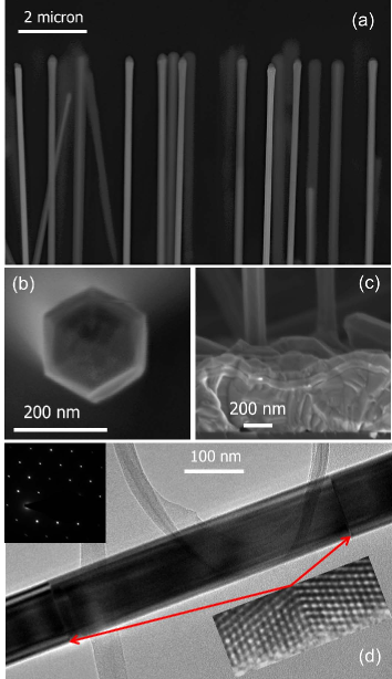
The GaAs/AlAs core/shell NWs were grown by molecular beam epitaxy (MBE) using the self-assisted vapor-liquid-solid (VLS) method 31, 32, 33, on (111)-oriented Silicon bearing a native oxide layer, using Ga, Al, and As4 as source materials. After water removal at C, the Si substrate was out-gassed at high temperature (C) in a separate chamber, before being transferred into the MBE growth chamber. The growth was initiated by condensation of Ga at the defects in the SiO2 layer and carried out at C and a group V/III ratio of . Uniform diameter GaAs NWs were grown along the ¡111¿ direction with a high aspect ratio (), no significant tapering and a pure zinc-blende structure, with only a few rotational twin planes, as revealed by careful transmission electron microscopy (TEM) analysis. For growth of the uniform nm AlAs shell and nm GaAs capping layer, the temperature was lowered to C. Figure 1(a) shows a side view of the top six microns of the as grown core/shell GaAs/AlAs NWs sample illustrating the uniform aspect ratio, typically obtained by self-assisted growth of GaAs NWs. The slightly larger thickness at the tip of the wires forms during the solidification of the gallium droplet. The NWs are otherwise very uniform in diameter all along microns. A top view scanning electron microscope (SEM) image of a single core/shell GaAs/AlAs can be seen in Figure 1(b) exhibiting a clear hexagonal cross section. At such high aspect ratio and high NWs density, one has to bare in mind the possibility of shadowing. We have excluded shadowing here by looking at the bulk growth in between the NWs, where the layers grown during the growth of the shell can clearly be seen by SEM (Figure 1(c)) in spite of the high aspect ratio () and the high density of NWs. Figure 1(d) shows a TEM image of a single core/shell GaAs/AlAs NW and a HR-TEM image of a single rotational twin plane occasionally found along such NWs. The electron diffraction (inset) confirms the existence of a ZB structure.
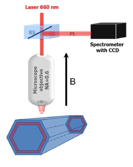
For the optical measurements, the NWs were dispersed onto a Si substrate with their ¡111¿ growth axis parallel to the surface. The average separation between wires is m to facilitate the investigation of the photoluminescence from individual NWs. The sample was placed in a micro-photoluminescence (-PL) setup containing piezoelectric translation stages and a microscope objective (see Figure 2). The -PL system was kept at a temperature of K in a cryostat placed in a resistive magnet producing a magnetic field of up to T. The field was applied in the Faraday configuration, perpendicular to the NW ¡111¿ growth axis. The PL of the NWs was excited with a diode laser at nm. Both the exciting and the collected light were transmitted through a monomode fiber coupled directly to the microscope objective. The diameter of the excitation beam was . The emission from the sample was dispersed in a spectrometer equipped with a CCD camera. The polarization resolved measurements were performed using free beam optics and a microscope objective. Several NWs have been investigated and all give almost identical results. In this letter we show representative results from our acquired data set.
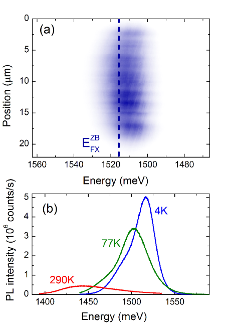
First we analyze the data obtained without magnetic field in order to characterize the investigated NWs. In Figure 3(a) a color plot of the PL spectra as a function of position along the NW is presented. Under the excitation conditions (power) used the observed emission energy is dominated by emission close to the energy of the free exciton recombination in GaAs (indicated in the figure by the solid blue line). Importantly, the spectra do not change as a function of position along the NW which confirms that it posses a pure ZB structure 9, 13. In Figure 3(b) we show the temperature dependence of the free exciton PL line. Here bright PL is observed even at room temperature, when we excite a small portion of a single NW (m out of a total length m i.e. only 5% of the NW). The emission, with around counts per second, saturates the CCD for integration times ms. Strong room temperature emission has previously been reported for macro-PL on a large number of ZB GaAs NWs with slightly different diameters and different lengths 34.
Linear polarization resolved measurements can also be used to differentiate between ZB and WZ structure. It is well established that for a pure ZB crystal structure for excitation and detection along the NW the free exciton emission is much stronger than for excitation and detection across the NW 35, 17. A strong polarization anisotropy was also observed in InP NWs 36 and is the result of the dielectric mismatch between the NW and its surrounding, which leads to the suppression of the component of the electric field perpendicular to the NW 35. This is not the case for NWs with WZ crystal structure, where the c-axis of the crystal is oriented along the long axis of the NW and the optical selection rules require that the free exciton emission is allowed only if the dielectric dipole moment is perpendicular to the c-axis of the crystal. This results in emission from WZ NWs which is strongly polarized across the NW 37, 38.
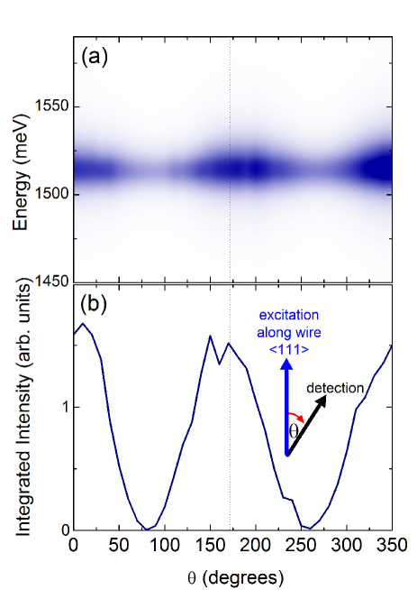
The measured linear polarization of the free exciton emission from the NW is presented in Figure 4(a-b). A linearly polarized excitation was used with the polarizer always aligned along the NW which corresponds to maximum PL emission. The linear polarization was analyzed by rotating the linear polarizer for detection with respect to the excitation polarizer. In Figure 4(a-b) the emission spectra as a function of angle are presented together with the integrated intensity. We observe minima in the amplitude of the collected emission for the configuration in which the polarization of the emission is orthogonal (crossed) with the polarization of the excitation, and maxima when the polarizers are parallel. Thus the polarization resolved measurements confirm that the investigated NW consists of a pure ZB structure.
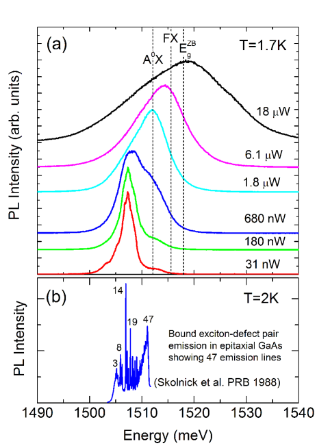
Typical -PL spectra of a single GaAs/AlAs core/shell NW measured for different excitation power are presented in Figure 5(a). The broken vertical lines indicate the recombination energy of an exciton bound to a neutral acceptor (A0X), a free exciton (FX) and the value of the epitaxial ZB GaAs band gap (E). In Figure 5(b) we show for comparison PL from high quality MBE grown GaAs measured by Skolnick and co-workers28, 29. Forty seven closely spaced lines are resolved in the original data (not all are visible in Figure5(b)), the energetic position of the lines is reproducible between different samples, and the strong line at 1.5069 eV (labeled 14) dominates the emission in all samples investigated28, 29. These lines were identified with emission from excitons bound to defect pairs with different separations. Confinement effects can be neglected for our nm diameter (core) NWs so that the PL results can be directly compared. We focus for the moment on the PL taken at the lowest power for which two lines are observed. The strong line at eV which we attribute to broadened emission from excitons bound to defect pairs (the energy corresponds almost exactly to the strong line 14 in the KP series). Indeed, upon closer inspection we find that this line consists of a double peak with a number of shoulders suggesting that it is made up of a large number of broadened lines. The weaker line around 1.514 eV can be associated with the recombination of an exciton bound to a neutral acceptor (). With increasing power the amplitude of the emission increases with respect to the bound exciton-defect pair emission with an increasing contribution from free exciton emission at higher powers. Further increase in the power induces a red shift of the free exciton emission towards the GaAs band gap energy presumably due to the screening of the exciton binding energy at high carrier densities. The line at eV associated with excitons bound to defect pairs was not observed in previously published data, possibly due to either the excitation power used or the larger linewidths9, 13.
Further support for our assignment of the eV line to bound exciton-defect pair recombination is provided by the PL data in magnetic fields as high as T. The spectra were acquired at K using low power excitation under which the line at 1.5069 eV dominates the zero field spectrum. In Figure 6 we show a color plot of the differential PL obtained by subtracting a suitably averaged PL spectra39. With increasing magnetic field the intensity of the emission increases dramatically, accompanied by a reduction in the line width. Several emission lines can be seen that exhibit a large diamagnetic shift () at low fields, which becomes linear in high magnetic fields. The observed energetic position and shift with magnetic field corresponds exactly to that of the strong line 14 of the bound exciton-defect pair recombination reported by Skolnick and co-workers,29 in high quality MBE grown GaAs, indicated by the symbols in Figure 6.
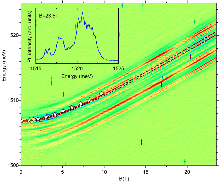
For T a Zeeman splitting of the lines is observed. This can be seen in more detail in Figure 7 where we have subtracted the large diamagnetic shift, by fitting the expression for the ground state of a two dimensional harmonic oscillator in perpendicular magnetic field, , to the strongest line at eV at T. Here is the harmonic trap frequency and is the cyclotron frequency. An excellent fit (dashed black lines in Figure 6) is achieved using meV and , which is reasonable for an effective mass electron weakly bound in a Coulomb potential. All of the observed emission lines have approximately the same slope at high magnetic fields demonstrating that the excitons involved, all have an orbital quantum number . The Zeeman splitting has been reproduced using an effective g-factor for an assumed effective spin of .
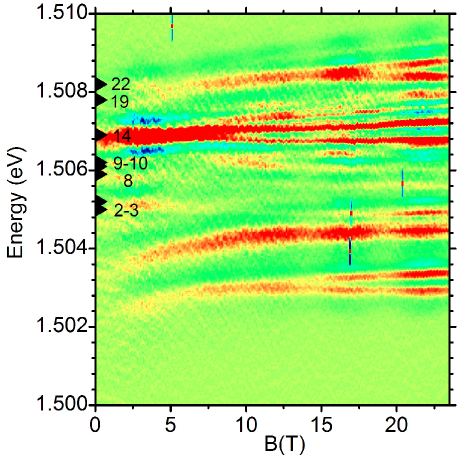
Strong features observed in the bound exciton-defect pair spectrum in GaAs are indicated by white arrow heads in Figure 7 and labeled using the notation of Skolnick and co-workers29. In Figure 7 at high magnetic fields some lines do not extrapolate correctly to zero field because their diamagnetic shift is slightly different from that of the 1.5069 eV line used for the correction. It should be noted that subtracting the diamagnetic shift has no effect on the energetic position of the lines at , which should be used for the comparison. Clearly our data reproduces quite nicely the prominent features of the bound exciton-defect pair spectrum of epitaxial GaAs.
In GaAs the Zeeman splitting of the peaks is well described using an effective spin Hamiltonian for an electron and a hole in orthorhombic symmetry involving isotropic and anisotropic hole g-factors together with crystal field parameters which can give rise to a zero field splitting29. In our measurements the magnetic field is applied perpendicular to the NW i.e. perpendicular to the ¡111¿ growth direction. However, the orientation of the magnetic field within the (111) plane is unknown so that we are unable to compare our results with the detailed predictions of the effective spin Hamiltonian.
To conclude, we have observed emission lines in the photoluminescence of single core/shell GaAs/AlAs NWs with a pure zinc-blende structure in the energy range eV. The magnetic field dependence of the emission allows us to unambiguously identify the emission with the recombination of excitons bound to defect pairs with different separations, previously observed only in very high quality MBE grown GaAs. This, together with the strong PL emission at room temperature demonstrates the very high optical quality of our GaAs NWs. The NWs, which can easily be dispersed onto a Si substrate, should open the way for numerous optoelectronic applications based on the well established Si device technology.
We would like to thank G. Kopnov for some help with the early stages of sample preparation, Ronit Popovitz-Biro for the TEM mesurements and I. Breslavetz for assistance with the PL measurements. Part of this work was supported by EUROMAGNET II under the SP7 transnational access program of the European Union under contract number 228043. We would also like to acknowledge partial support by the Israeli Science Foundation grant #530/08 and Israeli Ministry of Science grant #3-6799.
References
- Cui et al. 2000 Cui, Y.; Duan, X.; Hu, J.; Lieber, C. M. The Journal of Physical Chemistry B 2000, 104, 5213–5216
- Duan et al. 2003 Duan, X.; Huang, Y.; Agarwal, R.; Lieber, C. M. Nature 2003, 421, 241–245
- Garnett and Yang 2010 Garnett, E.; Yang, P. Nano Letters 2010, 10, 1082–1087, PMID: 20108969
- Lopez et al. 2009 Lopez, F. J.; Hemesath, E. R.; Lauhon, L. J. Nano Letters 2009, 9, 2774–2779, PMID: 19527044
- Fontcuberta i Morral et al. 2007 Fontcuberta i Morral, A.; Arbiol, J.; Prades, J.; Cirera, A.; Morante, J. Advanced Materials 2007, 19, 1347–1351
- Kriegner et al. 2011 Kriegner, D.; Panse, C.; Mandl, B.; Dick, K. A.; Keplinger, M.; Persson, J. M.; Caroff, P.; Ercolani, D.; Sorba, L.; Bechstedt, F.; Stangl, J.; Bauer, G. Nano Letters 2011, 11, 1483–1489
- Shtrikman et al. 2009 Shtrikman, H.; Popovitz-Biro, R.; Kretinin, A.; Houben, L.; Heiblum, M.; Bukala, M.; Galicka, M.; Buczko, R.; Kacman, P. Nano Letters 2009, 9, 1506–1510, PMID: 19253998
- Shtrikman et al. 2009 Shtrikman, H.; Popovitz-Biro, R.; Kretinin, A.; Heiblum, M. Nano Letters 2009, 9, 215–219
- Spirkoska et al. 2009 Spirkoska, D. et al. Phys. Rev. B 2009, 80, 245325
- Hoang et al. 2009 Hoang, T. B.; Moses, A. F.; Zhou, H. L.; Dheeraj, D. L.; Fimland, B. O.; Weman, H. Applied Physics Letters 2009, 94, 133105
- Heiss et al. 2011 Heiss, M.; Conesa-Boj, S.; Ren, J.; Tseng, H.-H.; Gali, A.; Rudolph, A.; Uccelli, E.; Peiró, F.; Morante, J. R.; Schuh, D.; Reiger, E.; Kaxiras, E.; Arbiol, J.; Fontcuberta i Morral, A. Phys. Rev. B 2011, 83, 045303
- Ketterer et al. 2011 Ketterer, B.; Heiss, M.; Livrozet, M. J.; Rudolph, A.; Reiger, E.; Fontcuberta i Morral, A. Phys. Rev. B 2011, 83, 125307
- Jahn et al. 2012 Jahn, U.; Lähnemann, J.; Pfüller, C.; Brandt, O.; Breuer, S.; Jenichen, B.; Ramsteiner, M.; Geelhaar, L.; Riechert, H. Phys. Rev. B 2012, 85, 045323
- Ketterer et al. 2011 Ketterer, B.; Heiss, M.; Uccelli, E.; Arbiol, J.; Fontcuberta i Morral, A. ACS Nano 2011, 5, 7585–7592
- Breuer et al. 2011 Breuer, S.; Pfuller, C.; Flissikowski, T.; Brandt, O.; Grahn, H. T.; Geelhaar, L.; Riechert, H. Nano Letters 2011, 11, 1276–1279
- Ahtapodov et al. 2012 Ahtapodov, L.; Todorovic, J.; Olk, P.; Mjaland, T.; Slattnes, P.; Dheeraj, D. L.; van Helvoort, A. T. J.; Fimland, B.-O.; Weman, H. Nano Letters 2012, 12, 6090–6095
- Titova et al. 2006 Titova, L. V.; Hoang, T. B.; Jackson, H. E.; Smith, L. M.; Yarrison-Rice, J. M.; Kim, Y.; Joyce, H. J.; Tan, H. H.; Jagadish, C. Applied Physics Letters 2006, 89, 173126
- Heim and Hiesinger 1974 Heim, U.; Hiesinger, P. Phys. Stat. Sol. (b) 1974, 66, 461
- Kunzel and Ploog 1980 Kunzel, H.; Ploog, K. Applied Physics Letters 1980, 37, 416–418
- Scott et al. 1981 Scott, G. B.; Duggan, G.; Dawson, P.; Weimann, G. Journal of Applied Physics 1981, 52, 6888–6894
- Briones and Collins 1982 Briones, F.; Collins, D. Journal of Electronic Materials 1982, 11, 847–866
- Temkin and Hwang 1983 Temkin, H.; Hwang, J. C. M. Applied Physics Letters 1983, 42, 178–180
- Eaves and Halliday 1984 Eaves, L.; Halliday, D. P. Journal of Physics C: Solid State Physics 1984, 17, L705–L709
- Contour et al. 1983 Contour, J. P.; Neu, G.; Leroux, M.; Chaix, C.; Levesque, B.; Etienne, P. Journal of Vacuum Science & Technology B: Microelectronics and Nanometer Structures 1983, 1, 811–815
- Heiblum et al. 1983 Heiblum, M.; Mendez, E. E.; Osterling, L. Journal of Applied Physics 1983, 54, 6982–6988
- Rao et al. 1985 Rao, E. V. K.; Alexandre, F.; Masson, J. M.; Allovon, M.; Goldstein, L. Journal of Applied Physics 1985, 57, 503–508
- Skromme et al. 1984 Skromme, B. J.; Stillman, G. E.; Calawa, A. R.; Metze, G. M. Applied Physics Letters 1984, 44, 240–242
- Skolnick et al. 1985 Skolnick, M. S.; Harris, T. D.; Tu, C. W.; Brennan, T. M.; Sturge, M. D. Applied Physics Letters 1985, 46, 427–429
- Skolnick et al. 1988 Skolnick, M. S.; Halliday, D. P.; Tu, C. W. Phys. Rev. B 1988, 38, 4165–4179
- Charbonneau and Thewalt 1990 Charbonneau, S.; Thewalt, M. L. W. Phys. Rev. B 1990, 41, 8221–8228
- Colombo et al. 2008 Colombo, C.; Spirkoska, D.; Frimmer, M.; Abstreiter, G.; Fontcuberta i Morral, A. Phys. Rev. B 2008, 77, 155326
- Fontcuberta i Morral et al. 2008 Fontcuberta i Morral, A.; Spirkoska, D.; Arbiol, J.; Heigoldt, M.; Morante, J. R.; Abstreiter, G. Small 2008, 4, 899–903
- Krogstrup et al. 2010 Krogstrup, P.; Popovitz-Biro, R.; Johnson, E.; Madsen, M. H.; Nygard, J.; Shtrikman, H. Nano Letters 2010, 10, 4475–4482
- Dhaka et al. 2012 Dhaka, V.; Haggren, T.; Jussila, H.; Jiang, H.; Kauppinen, E.; Huhtio, T.; Sopanen, M.; Lipsanen, H. Nano Letters 2012, 12, 1912–1918
- Ruda and Shik 2005 Ruda, H. E.; Shik, A. Phys. Rev. B 2005, 72, 115308
- Wang et al. 2001 Wang, J.; Gudiksen, M. S.; Duan, X.; Cui, Y.; Lieber, C. M. Science 2001, 293, 1455–1457
- Mishra et al. 2007 Mishra, A.; Titova, L. V.; Hoang, T. B.; Jackson, H. E.; Smith, L. M.; Yarrison-Rice, J. M.; Kim, Y.; Joyce, H. J.; Gao, Q.; Tan, H. H.; Jagadish, C. Applied Physics Letters 2007, 91, 263104
- Birman 1959 Birman, J. L. Phys. Rev. Lett. 1959, 2, 157–159
- 39 A moving window average over 10-50 pixels is subtracted from each spectrum. This produces a result which is almost indistinguishable from the numerical second derivative and serves to highlight small features (peaks) on a large background.