Spin Pumping and Inverse Spin Hall Effect in Germanium
Abstract
We have measured the inverse spin Hall effect (ISHE) in n-Ge at room temperature. The spin current in germanium was generated by spin pumping from a CoFeB/MgO magnetic tunnel junction in order to prevent the impedance mismatch issue. A clear electromotive force was measured in Ge at the ferromagnetic resonance of CoFeB. The same study was then carried out on several test samples, in particular we have investigated the influence of the MgO tunnel barrier and sample annealing on the ISHE signal. First, the reference CoFeB/MgO bilayer grown on SiO2 exhibits a clear electromotive force due to anisotropic magnetoresistance and anomalous Hall effect which is dominated by an asymmetric contribution with respect to the resonance field. We also found that the MgO tunnel barrier is essential to observe ISHE in Ge and that sample annealing systematically lead to an increase of the signal. We propose a theoretical model based on the presence of localized states at the interface between the MgO tunnel barrier and Ge to account for these observations. Finally, all of our results are fully consistent with the observation of ISHE in heavily doped -Ge and we could estimate the spin Hall angle at room temperature to be 0.001.
I Introduction
The first challenging requirement to develop semiconductor (SC)
spintronicsZutic2004 ; Awschalom2007 i.e. using both carrier charge and spin in electronic
devices consists in injecting spin polarized electrons in the
conduction band of a SC at room temperature. SCs should be further
compatible with silicon mainstream technology for implementation in
microelectronics making silicon, germanium and their alloys among
the best candidates.Zutic2011 In Si, due to low spin-orbit coupling, very
long spin diffusion lengths were predicted and measured
experimentally.Dash2009 ; Jonker2007 ; Appelbaum2007 ; Suzuki2011 Germanium exhibits the same crystal inversion
symmetry as Si, a low concentration of nuclear spins but higher carrier
mobility and larger spin-orbit coupling which should allow in
principle spin manipulation by electric fields such as the Rashba
field.Zhou2011 ; Jain2011 ; Saito2011 ; Jeon2011 ; Hanbicki2012 So far in order to perform spin injection from a
ferromagnetic metal (FM) into Si or Ge, one needs to overcome at least
three major obstacles: (i) the conductivity mismatch which requires
the use of a highly-resistive spin-conserving interface between the
FM and the SC,Fert2001 (ii) the Fermi level pinning at the SC surface due
to the presence of a high density of interface states and the
interface spin flips which are generally associatedDash2009 ; Jain2011 ; Tran2009 and
finally (iii) the presence of random magnetic stray fields created by
surface magnetic charges at rough interfaceJain2011 ; Dash2011 around which the electrically
injected spins are precessing and partly lost by decoherence. In
this work, we have inserted a thin MgO tunnel barrier between Ge and
the CoFeB ferromagnetic electrode in order to: (i) circumvent the
conductivity mismatch and (ii) partly alleviate Fermi level pinning
by strongly reducing the interface states densityCantoni2011 ; Lee2010 ; Zhou2010 which leads
to a modest Schottky barrier height at the MgO/n-Ge interface. We
have then investigated the spin injection mechanisms using the so called
three-terminal device.Dash2009 In this geometry, the same ferromagnetic
electrode is used for spin injection and detection. This three-terminal device used
in non-local geometry represents a simple and unique tool to probe spin
accumulation both into interface states and in the SC channel.Dash2009 ; Jain2011 ; Li2011 In particular, we could measure spin injection in the silicon and germanium conduction bands at room temperature.Jain2012 ; Jain2013
The spin Hall angle (, ratio between the transverse
spin current density and the longitudinal charge current density)
Vila2007 is a key material parameter to develop new kinds of devices based on the spin Hall effect (SHE). The SHE is the conversion of a charge current into a spin current via the spin-orbit interaction. Conversely the inverse spin Hall effect (ISHE) is the conversion of a spin current into a charge current. Several methods have been developed to determine quantitatively : pure
magnetotransport measurements on lateral spin valves (LSV),Vila2007 ; Valenzuela2006 ; Morota2011 ferromagnetic
resonance (FMR) along with spin pumping (SP-FMR)
Ando2011a ; Mosendz2010b ; Azevedo2011 and spin torque FMR
(ST-FMR) Liu2011 on ferromagnetic/non-magnetic bilayers
(FM/N). Recently could be estimated in and -GaAs Ando2011b as well as in -Si Shikoh2013 by spin pumping and inverse spin Hall effect. The precession of the FM layer in direct contact with the SC has been excited by microwaves which pumps a spin current into the SC. The spin current was then detected by inverse spin Hall effect. In that case, the interface resistance to overcome the conductivity mismatch issue was given by the reminiscent Schottky barrier at the FM/SC interface. Here we have similarly used a combined SP-FMR method to study inverse spin Hall effect in germanium. In the first section, we describe the sample preparation and the experimental techniques. In the second section, the phenomenological models for the ferromagnetic resonance and electromotive force are presented. Finally the experimental results are shown and discussed in sections 3 and 4 respectively. In particular, we propose a microscopic model based on the presence of localized states at the MgO/Ge interface to explain the spin pumping mechanism in our system. We finally discuss about the influence of the MgO tunnel barrier and sample annealing on the ISHE signal.
II Sample preparation
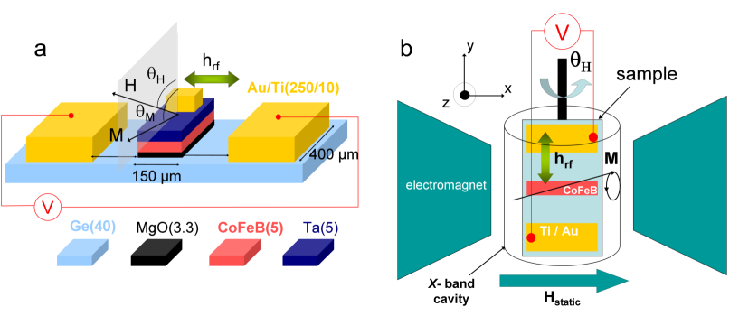
The multi-terminal device we initially used for electrical spin injection, detection and manipulationJain2012 is made of a full stack Ta(5 nm)/CoFeB(5 nm)/MgO(3 nm) grown by sputtering on a 40 nm-thick germanium film on insulator (GOI).Jain2011 GOI wafers are made of a Si + degenerate substrate and a 100 nm-thick SiO2 layer (BOX). They were fabricated using the Smart CutTM process and Ge epitaxial wafers.Deguet2005 The transferred 40 nm-thick Ge film was -type doped in two steps: a first step (phosphorus, cm-2, 40 keV, annealed for 1h at 550∘C) that provided uniform doping in the range of 1018 cm-3, and a second step (phosphorus, cm-2, 3 keV, annealed for 10 s at 550∘C) that increased surface + doping to the vicinity of 1019 cm-3. The thickness of the n+-doped layer is estimated to be 10 nm. The GOI surface was finally capped with amorphous SiO2 to prevent Ge from surface oxidation. The tunnel barrier and ferromagnetic electrode were then fabricated from magnesium (Mg, 1.1nm) and cobalt-iron-boron (Co60Fe20B20, 5nm) layers deposited by conventional DC magnetron sputtering onto germanium (Ge) after removing the SiO2 capping layer using hydrofluoric acid and de-ionized water. The deposition rates were respectively of 0.02 nm.s-1 and 0.03 nm.s-1 at an argon pressure of mbar. The base pressure was mbar. All the depositions were performed at room temperature. The oxidation of the insulating barrier was performed by plasma oxidation, exposing the Mg metallic layer to a 30 seconds radio-frequency oxygen plasma at a pressure of mbar and a radio-frequency power of 100 W. Three successive Mg deposition plus oxidation steps were achieved ([Mg 1.1 / oxidation]3) to grow a 3.3 nm thick MgO layer. The sample annealings were performed under 10-7 mbar at 300∘C for 90 minutes. The ferromagnetic layer is then capped with 5 nm of Ta to prevent oxidation. After depositing the spin injector, samples have been processed using standard optical lithography. In a first step, we define the ferromagnetic electrode ( m2) and ohmic contacts ( m2 on Ge and m2 on top of the ferromagnetic electrode). In a second step, the germanium channel is etched down to the BOX to form a mesa of 1070 m long and 420 m large. Finally soft argon etching is used to remove the top 10 nm-thick n+-doped germanium layer. The whole device is shown in Fig. 1(a). In order to test the influence of the MgO tunnel barrier (resp. sample annealing), similar devices without MgO (resp. without annealing) were processed and studied. Ferromagnetic resonance and inverse spin Hall effect measurements were performed in a Brüker ESP300E -band CW spectrometer with a cylindrical Brüker ER 4118X-MS5 cavity. The measurement geometry is depicted in Fig. 1(b). Complementary measurements of FMR lines at different frequencies between 2 and 24 GHz were performed in a stripe-line vector network analyzer system.
III Ferromagnetic resonance and electromotive force
III.1 Ferromagnetic resonance (FMR)
Fig. 2(a) shows a schematic drawing of the reference sample and the definition of the magnetization and external magnetic field polar angles, and , respectively. The reference sample is made of a single CoFeB layer grown on SiO2 as follows: Ta(5nm)/CoFeB(5nm)/MgO(3.3nm)//SiO2. We have inserted a thin MgO oxide layer between CoFeB and SiO2 in order to make a comparison with the Ta(5nm)/CoFeB(5nm)/MgO(3.3nm)/Ge system studied in the next sections.
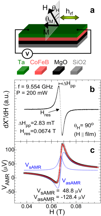
From FMR measurements (Fig. 2(b)), we can determine the peak-to-peak linewidth and the resonance field. By sweeping the external magnetic field H under a microwave excitation of frequency , the resonance condition is achieved in a ferromagnetic film when:Smit1955
| (1) |
where is the precession angular frequency, is the gyromagnetic ratio with the Landé factor , is the reduced Planck constant, is the Bohr magnetron and is the saturation magnetization of the ferromagnetic film. The second order partial derivatives of the free energy density are evaluated at the equilibrium angles and of the magnetization M for which: and . The shape anisotropy in a ferromagnetic polycristalline film ( ) is usually much larger than in-plane crystalline anisotropy. By recording FMR spectra with the DC magnetic field in the film plane at different azimuthal angles (not shown), we could demonstrate that in-plane anisotropy in the CoFeB electrodes used in this work is indeed negligible with respect to shape anisotropy. Thus we can consider that the free energy density is given by:
| (2) |
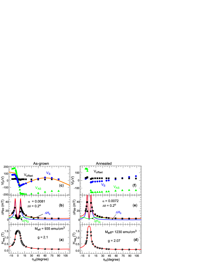
where the first term is the Zeeman energy and the second one accounts for shape anisotropy and any other perpendicular uniaxial anisotropy . The effective saturation magnetization is thus defined as: . By minimizing numerically we can obtain the magnetization equilibrium angles: and . The resonance field is then given by combining Eq. (1) and (2), it can be plotted as a function of the external static field orientation () and the excitation frequency as shown in Fig. 3. and are extracted from the out-of-plane (OOP) angular dependence of the resonance field using a least square fit (as shown for instance in Fig. 4(a,d)).

Analytical solutions of can be obtained for the parallel, , and perpendicular, , cases. In the parallel case, we find:
| (3) |
The frequency dependence of the FMR linewidth also allows calculating the Gilbert damping constant using the following expression:Heinrich1985
| (4) |
where the peak-to-peak linewidth, ,is measured when is applied parallel to the film plane (). The term accounts for the frequency-independent contributions due to inhomogeneities in the ferromagnetic layer and is the FMR linewidth due to the Gilbert damping. As shown experimentally in section IV, at high frequency and we systematically neglect this contribution to the FMR linewidth. Moreover, the OOP angular dependence of the peak-to-peak linewidth at a given frequency can be written:
| (5) |
where the Gilbert contribution can be calculated from:Goryunov1995 , and is the angular dispersion of the perpendicular anisotropy and demagnetizing field () due to inhomogeneities in the FM layer. We show in the following that and can be extracted from the frequency and OOP angular dependences of .
III.2 Electromotive force measured on the reference sample
The electromotive force generated in the ferromagnetic layer and shown in Fig. 2(c) is simultaneously recorded with the FMR spectrum. The origins of this electromotive force are the anisotropic magnetoresistance (AMR) Ando2011a ; Mosendz2010b ; Azevedo2011 and anomalous Hall effect which manifest at the resonance field. At the resonance field, the precessing magnetization induces a time varying resistivity of the ferromagnetic layer which combines with the radiofrequency induced currents (along in Fig. 1(b)) to produce a DC voltage. The radiofrequency currents are likely produced within the metallic layer by the non-vanishing radiofrequency electric field in the cavity at the sample level. In our set-up geometry, the electromotive force is measured as a voltage along (see Fig. 1(b)) and thus in the transverse Hall geometry. Therefore we measure the planar Hall effect (PHE) and the anomalous Hall effect (AHE) in CoFeB. It was proposed and shown by Azevedo et al. Azevedo2011 and Harder et al. Harder2011 that the resulting voltage is well described by both a symmetric and an asymmetric contributions. In the CoFeB reference film, the asymmetric component is dominant. The electromotive force can be written as (see Appendix A):
| (6) | |||||
where (resp. ) is the amplitude of the symmetric (resp. asymmetric) contribution to the electromotive force. We have taken into account a non-resonant offset voltage , is the resonance field and . where is the phase shift between the radiofrequency current and the magnetization.Azevedo2011 ; Harder2011 The symmetric and asymmetric contributions as well as the offset voltage are proportional to the microwave power. It means that , , and are proportional to , where is the microwave magnetic field strength.
III.3 Spin pumping and inverse spin Hall effect in germanium
Here we consider the device shown in Fig. 1. Under radiofrequency excitation the magnetization precession of the ferromagnetic layer pumps spins to the non-magnetic germanium layer (N) and the corresponding spin current generates an electric field in Ge due to ISHE: . is the spin-current density along and its spin polarization vector. This electric field is converted into a voltage between both ends of the Ge channel.Ando2011a In the case of germanium we overcome the conductivity mismatch issue by inserting a thin MgO tunnel barrier (I) between Ge and CoFeB. This additional interface resistance allows for spin accumulation in the germanium conduction band. As a consequence of spin pumping, the damping constant, , is enhanced with respect to the one of the reference sample, . The real part of the tunnel spin mixing conductance, , is given by:Tserkovnyak2005 ; Mosendz2010b
| (7) |
where is the CoFeB thickness. When the static magnetic field is applied parallel to the interface (=90∘), the spin-current density at the interface between CoFeB/MgO and Ge, is given by:Ando2011a
| (8) |
where is the strength of the microwave magnetic field into the resonance cavity. is calculated by measuring the factor of the resonance cavity , where is the width at half maximum of the frequency distribution when the sample is placed into the cavity. To measure we use a second frequencemeter in series with the first one. The voltage due to the inverse spin Hall effect is always symmetric with respect to the resonance field and its amplitude is discussed in Ref. Ando2011a ; Mosendz2010b ; Azevedo2011 . We then modify the equivalent circuit used in Ref. Ando2011a and refined the model used in Ref. Jain2012 to account for electron transport through the tunnel and Schottky barriers back to the FM (see Appendix B). Then the ISHE voltage in our system is given by:
| (9) |
where is the width of the ferromagnetic electrode (150 m), (resp. ) is the Ge (resp. Ta/CoFeB) thickness, (resp. ) is the Ge (resp. Ta/CoFeB) conductivity. where and (resp. and ) are the thickness and conductivity of the CoFeB (resp. Ta) layer. depends on the resistance-area product of the interface between CoFeB/MgO and Ge as:
| (10) |
In order to estimate the magnitude, the electromotive force and the ferromagnetic spectrum are measured simultaneously. The measured voltage might have one symmetric, , one asymmetric, , and one offset contributions. The raw data will be fitted with:
| (11) |
IV Results
IV.1 Reference sample
Fig. 4 shows the OOP dependence of the resonance field, peak-to-peak linewidth and electromotive force on the as-grown and annealed Ta(5nm)/CoFeB(5nm)/MgO(3.3nm)//SiO2 reference samples. From the angular dependence of , we obtain the effective saturation magnetization () and the factor and from we obtain the damping constant () and the angular dispersion (). The angular dependence of the peak-to-peak linewidth can be calculated using the following method: after fitting numerically the OOP dependence of the resonance field (Fig. 4(a,d)) we use and to calculate the theoretical dispersion relationship between and the external magnetic field for different angles. This is shown in Fig. 3 where the dotted line corresponds to the frequency at which the measurements are performed. The intercept of each curve with the dotted line gives the value of the resonance field along with the equilibrium polar angle of at different values. The OOP linewidth angular dependence is shown in Fig. 4(e) and fitted using Eq. (5). In addition, in Fig. 4(c), we have used the formula of Appendix A to fit the OOP angular dependence of the symmetric voltage contribution to the electromotive force in the as-grown reference sample. The OOP angular dependence of the symmetric voltage in the Ge-based device () clearly shows a different behavior (see Fig. 10(c) and 10(f)).
We have also recorded the power dependence of both the FMR signal and the electromotive force when is applied parallel to the film plane. The results are shown in Fig. 5. The electromotive force was fitted according to Eq. (6). and depend linearly on the applied power in the whole power range whereas slightly deviates from the linear behavior for high powers. Nevertheless we note that in both reference samples. The sample sizes are mm2 for the as-grown sample and mm2 for the annealed one. For the same RF power of 200 mW and the field applied parallel to the film plane (=90∘), we found -159 for the as-grown sample and -64.2 for the annealed one. Since depends linearly on the ferromagnetic electrode width, we can estimate the expected value for the CoFeB bar of Fig. 1(a): 6.8 for the as-grown sample and 6.4 for the annealed one. The expected symmetric contribution to the electromotive force will then be almost one order of magnitude less. Furthermore, in the device of Fig. 1, the electrical contacts are no more made on the metallic multilayer, as show in Fig. 2(a), but on Au/Ti ohmic contacts on top of Ge which would reduce the PHE and AHE contributions.
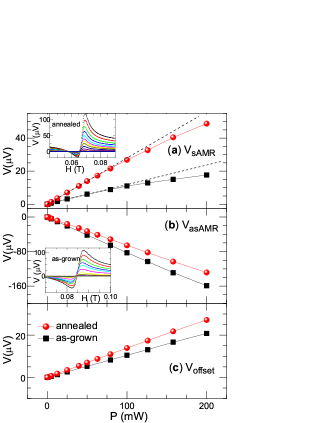
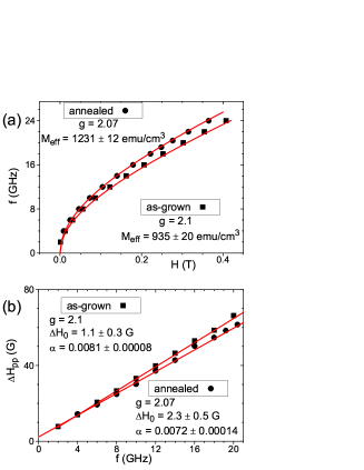
Fig. 6 shows the frequency dependence of the resonance field (a) and peak-to-peak linewidth (b) of the as-grown and annealed reference samples. In both figures, we have used the factors deduced from the OOP angular dependence of (see Fig. 4(a) and 4(d)) and adjusted the and values according to eq. (3) and (4) respectively to fit the curves. The frequency independent part of the peak-to-peak linewidth which is due to inhomogeneities in the magnetic layer is very weak in both samples. We find 1.1 Oe for the as-grown sample and 2.3 Oe for the annealed one which confirms that at a frequency close to 9 GHz. Moreover the effective perpendicular anisotropy (4) increases from 1.175 T up to 1.545 T upon annealing as recently reported.Wang2011 Both samples exhibit very low damping constants comparable to the ones found in Ref. Liu2011JAP . Interestingly the peak-to-peak linewidth and damping constants decrease upon annealing in contrast with other results.Chen2012 It means that we have effectively reduced the intrinsic inhomogeneities of the CoFeB electrode by annealing. In particular, the annealing process did not promote chemical inter-diffusion at the interfaces with CoFeB as found in thinner CoFeB films in magnetic tunnel junctions.Yang2012
IV.2 Spin pumping at the ferromagnet/Germanium interface
IV.2.1 CoFeB/Ge Interface
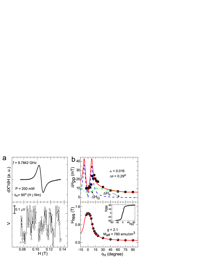
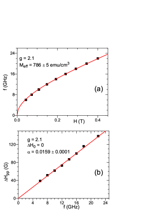
In this section, we consider the device shown in Fig. 1(a) where the CoFeB electrode has been directly grown on the Ge film without tunnel barrier. The FMR line and the corresponding electromotive force are shown in Fig. 7(a). A clear absorption is observed in the FMR spectrum whereas the electromotive force at the resonance field is negligible. Hence, in the measuring geometry of Fig. 1(a) where the voltage is directly probed on the germanium layer, we do not detect the PHE and the AHE in the CoFeB ferromagnetic layer at the resonance. The angular dependence of the resonance field and peak-to-peak linewidth are displayed in Fig. 7(b). The frequency dependence of and are shown in Fig. 8. First, the effective CoFeB saturation magnetization is lower than in the reference sample: this is probably due to the intermixing between CoFeB and Ge at the interface. In the same way, the larger damping constant may be due to interface inhomogeneities as a consequence of intermixing and not to spin pumping since no electromotive force is observed. We have then performed the same measurements on the annealed sample. In that case, both the ferromagnetic resonance signal and the electromotive force vanish and the CoFeB film has completely diffused into the Ge layer. These results show that the MgO tunnel barrier is not only necessary to overcome the conductivity mismatch issue but also to prevent the intermixing between CoFeB and Ge at the interface.
IV.2.2 CoFeB/MgO/Ge Interface
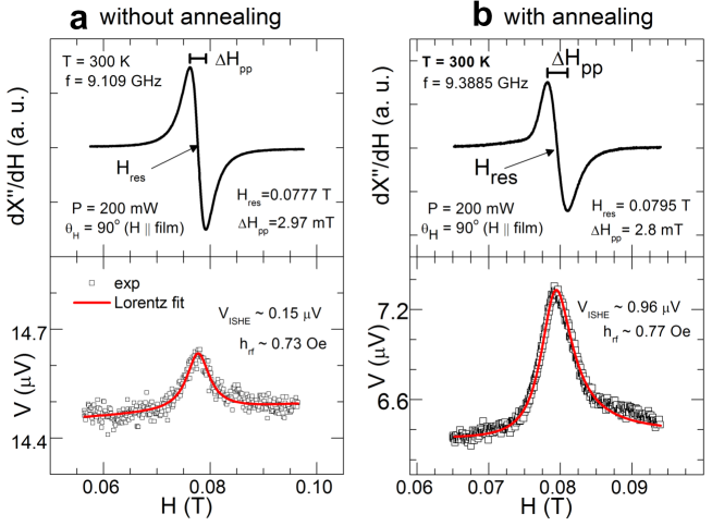
We now consider the same device as in the previous section but with a thin MgO tunnel barrier inserted between CoFeB and Ge as shown in Fig. 1(a). The FMR spectrum and the corresponding electromotive force are shown in Fig. 9(a) for the as-grown sample and Fig. 9(b) for the annealed one. Here a clear electromotive force is detected at the resonance field in both cases. The red line is the fit according to Eq. (11) considering a single symmetric contribution. Moreover by annealing we observe an enhancement of the electromotive force signal. In Fig. 10, the OOP angular dependence of the resonance field, peak-to-peak linewidth and the amplitude of the electromotive force of both samples are displayed. Like in the previous section, the complete analysis of these data yields , , , and . The solid lines in Fig. 10(c) and Fig. 10(f) are fits according to the formula:Ando2011b .
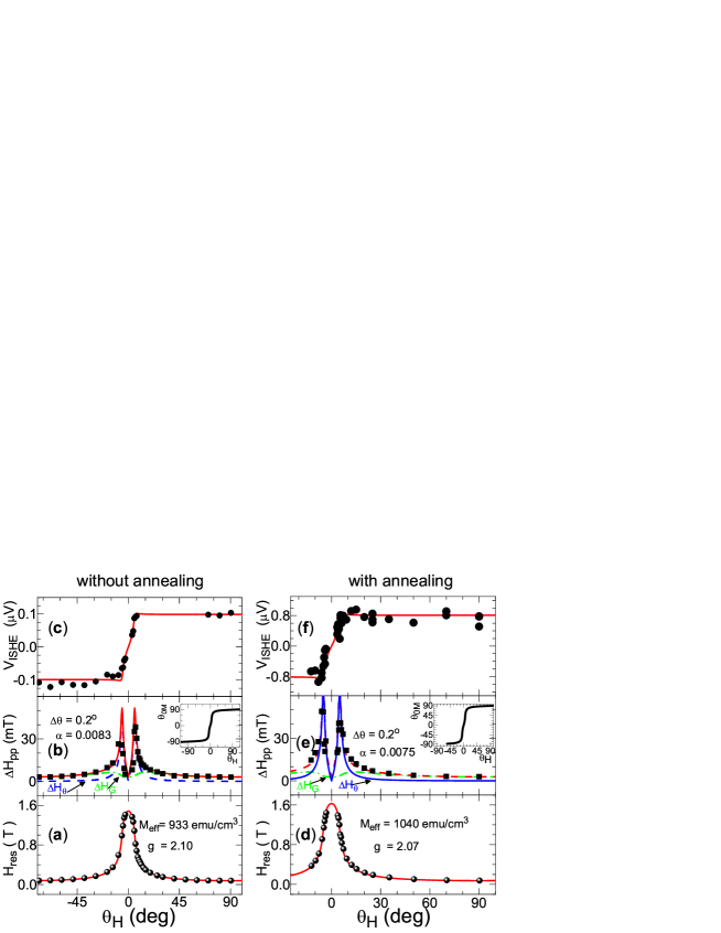
We also measured the FMR spectrum in the parallel case at different frequencies on both devices (not shown). The frequency dependence of always shows a linear behavior with a very low value showing that the Gilbert-type effect is the dominating contribution to the damping in all the samples studied.
In Table 1, we can clearly see that the annealing process increases the perpendicular magnetic anisotropy of the system (enhancement of ) and reduces the intrinsic damping constant. Spin pumping in Ge leads to an increase of the damping constant () with respect to that of the reference system ().
| () | |||||
|---|---|---|---|---|---|
| CoFeB/MgO ref. | n-Ge device | CoFeB/MgO ref. | n-Ge device | ||
| as-grown | |||||
| annealed | |||||
The power dependence of the amplitude when the external DC magnetic field is applied parallel to the FM layer is shown in Fig. 11 where the solid line is a linear fit. Such linear behavior accounts well for the dependence of the VISHE since the microwave power is proportional to the square of the rf magnetic field ().
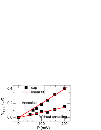
All these results support the fact that the measured electromotive force is due to spin pumping from the CoFeB electrode and inverse spin Hall effect in germanium.
IV.2.3 Estimation of the spin Hall angle in n-Ge at room temperature
In order to estimate the spin Hall angle in -Ge, we have calculated the tunnel spin mixing conductance according to Eq. (7). We found: for the device with the as-grown CoFeB layer and for the device with the annealed CoFeB layer. The spin-current density at the interface , when =90∘, is calculated using Eq. (8) where the CoFeB effective saturation magnetization , the gyromagnetic ratio , and the damping factor were deduced from FMR measurements. The results are reported in Table 2. For a power of 200 mW, the microwave magnetic field () was measured with the sample inside the resonator cavity. The amplitude is calculated according to Eq. (9) with the width of the ferromagnetic electrode =150 m, the FM thickness nm, the Ge channel thickness =40 nm and the conductivities and the resistance-area product of the interfase given in Table 2. The spin diffusion length in the semiconductor channel is 1.3 m (Ref. Jain2012 ). The conductivities (including the interface value) and the spin diffusion length were measured independently on the same device (Ref. Jain2012 ).
| Not annealed | annealed | |
| ) | 0.6 | 1.0 |
| (G) | 0.73 | 0.77 |
| () | 0.047 | 0.11 |
| 9440 | 1250 | |
| 270 | 270 | |
| 1.047 | 1.085 | |
| 0.0011 | 0.00044 |
We then estimate the spin Hall angle in -Ge from the annealed sample at room temperature: , which is of the same order of magnitude as in -GaAs (0.007 in Ref. Ando2011b ) and one order of magnitude larger than in -Si (0.0001 in Ref. Ando2012 ). In a similar way we could estimate the spin Hall angle in -Ge using the data from the as-grown sample and found: 0.00044. Such a difference might come either from the error bars and/or from the phenomenological model we have used here. We have measured several annealed devices from the same batch and found between 0.0010 and 0.0012 which gives an estimation of the error bar. We thus conclude that the phenomenological model we use to estimate is not adapted to our system. In particular, this model does not account for the presence of interface states between MgO and Ge. We have shown in a previous work that interface states play a crucial role in the spin injection mechanism.Jain2012 Electrical spin injection into Ge proceeds by two-step tunneling: the electrons tunnel from the FM to the localized interface states (IS) through the MgO barrier and from the IS to the Ge conduction band through the Schottky barrier. Because spin flips occur into interface states, the spin accumulation (hence the spin current) is drastically reduced in the Ge conduction band. By annealing, the density of interface states is reduced and direct spin injection into the Ge conduction band is favored. As a consequence, the spin current in the as-grown sample is reduced as compared to the spin current in the annealed sample which leads to the underestimation of as found experimentally. We thus give in the next section a microscopic model accounting for the presence of the tunnel barrier and interface states to accurately describe spin pumping and ISHE in germanium.
V Discussion
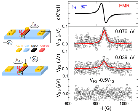
In the as-grown and annealed CoFeB/MgO/Ge samples, we could clearly measure an electromotive force due to ISHE at the ferromagnetic resonance of CoFeB. This photovoltage has a symmetric Lorentzian shape. Furthermore we have shown that all our findings are in good agreement with the observation of ISHE: symmetrical behaviour of around the resonance field , =0 when the external magnetic field is applied perpendicular to the film (=0) , changes its sign when crossing =0 (Fig. 10), and finally the linear dependence of its amplitude with the microwave power excitation (Fig. 11). This result clearly demonstrates the presence of both spin accumulation and related spin current in the Ge conduction band at room temperature. It was also supported by temperature dependent measurements in a previous work.Jain2012 In order to confirm that the photovoltage we measure is really due to ISHE and rule out any spurious effects, we carried out complementary measurements. First we studied the photovoltage in millimeter-sized reference samples (both as-grown and annealed) made of CoFeB/MgO/SiO2 with the voltage probes directly connected to the CoFeB film. In that case, we found a dominant asymmetric voltage contribution with respect to the resonance field. It corresponds to the planar Hall effect in the ferromagnet as a combination of anisotropic magnetoresistance and the rf current induced in the ferromagnet by the non-vanishing electric field from the cavity (see Appendix A). This asymmetric voltage contribution due to PHE could not be detected on the device of Fig. 1 with Ge. Moreover the out-of-plane angular dependence of this weak symmetric voltage on the reference sample is different from that of the symmetric voltage we detected in the device of Fig. 1 with Ge. To summarize this study on the reference sample, we can claim that the symmetric photovoltage observed in CoFeB/MgO/Ge samples is due to ISHE and not to PHE in the ferromagnet. We also carried out the same measurements on CoFeB/Ge samples to study the effect of the MgO tunnel barrier. Without MgO tunnel barrier, we never detected a photovoltage in Ge. It first proves that the photovoltage due to the PHE in CoFeB is undetectable in Ge. It also shows that the MgO tunnel barrier is necessary to perform spin injection in Ge by spin pumping. Furthermore, as shown in Fig. 12, we have recorded several voltages on the same CoFeB/MgO/Ge device at the ferromagnetic resonance in order to estimate the tunneling spin Seebeck effect.LeBreton2012 ; Jain2012b Indeed at the ferromagnetic resonance, the CoFeB electrode absorbs part of the incident microwave power which increases its temperature. As a consequence, a vertical temperature difference may appear between the CoFeB electrode and the Ge layer. This temperature gradient may create a tunneling Seebeck voltage and a tunneling spin Seebeck voltage which is only a few percents of the Seebeck voltage.Jeon2012 The resulting spin current gives rise to ISHE in germanium just like spin pumping. In order to discriminate between spin pumping and the tunneling spin Seebeck effect, we measured the following voltages at the FMR: , and shown in Fig. 12. The sum of the tunneling Seebeck and tunneling spin Seebeck voltages () is given by: or . As shown in Fig. 12, is negligible (below the noise level) which rules out the presence of tunneling spin Seebeck at the ferromagnetic resonance in our system. Therefore spin injection in Ge proceeds by spin pumping and not by tunneling spin Seebeck effect.
We now address the important issue of the microscopic origin of spin pumping effects in Ge through a MgO tunnel barrier from a theoretical point of view. As demonstrated below, the origin of spin pumping into SCs through a tunnel barrier lies in the evanescent but however non-zero exchange coupling between a band of localized states (LS) and the ferromagnet through the tunnel barrier, nonetheless sufficiently transparent. Indeed, spin-pumping tserkovnyak2002 ; Tserkovnyak2005 in metallic tunnel junctions is expected to fall-off in the absence of any exchange field experienced from the ferromagnet (FM) by the delocalized carriers injected in the non-magnetic metal (N). On the other hand, spin injection into a SC by electrical means, as well as by spin-pumping, requires a tunnel barrier at the interface between both types of materials rashba2000 ; Fert2001 in order to overcome the impedance mismatch issue schmidt2000 describing a total diffusive spin current backflow towards the FM. As shown in our experiments, spin-pumping in a semiconductor with a tunnel barrier can be recovered with some conditions. First, the carriers injected by tunneling from a FM contact have to remain localized at the interface between the tunnel barrier and the semiconductor in the timescale of a single magnetization precession. Second, the effective tunnel exchange field experienced by the carriers, that we call hereafter , has to be large enough for the spin to rotate in a timescale of a magnetization precession. These two necessary conditions may be fulfilled within a two-step tunneling picture of spin injection into evanescent (or localized states) Tran2009 and in the limit of an effective exchange field larger than a certain lower bound. This will be demonstrated below. The third condition to observe spin-pumping in FM/tunnel barrier/SC systems is a minimum value for the conductance of the Schottky barrier delimiting the two regions i.e the evanescent states and the SC channel. A thermal activation may be needed to fulfill this third condition. We thus give an analytical expression for the source term taking into account a two-step tunneling process.
Let us consider the standard theory of spin-pumping at the FM/N interface. The source term is known to be equal to:tserkovnyak2002 ; Tserkovnyak2005
| (12) |
in the case of a FM/N ohmic contact where is the unit magnetization vector and the complex spin mixing conductance. The spins pumped into N then create a diffusive spin current backflow to the FM according to the three-dimensional spin-dependent transmission matching at the FM/N interface:brataas2006
| (13) |
where , in N and , in FM are respectively the charge and spin accumulations at the interface. is the sum of spin-up and spin-down conductances and is the interfacial spin asymmetry coefficient. This backflow of spin current results in a down-renormalization of the spin current pumped in the non magnetic material as shown in a recent couple of papers.bauer2012 ; vanwees2012 The exact form of the corresponding down renormalization has to be considered case by case.
The new source term describing spin-pumping in a broad band of evanescent states at the tunnel barrier/SC interface has to involve a small but however non-zero exchange interaction between localized states and the magnetization (of unit vector ) of the FM through the tunnel barrier; this exchange interaction couples evanescent wavefunctions inside the barrier. In the following, we will define in the form: where is the bare on-site exchange interaction of the order of the exchange interaction in FM or even larger (about 1 eV), is the imaginary electronic wavevector in the barrier and the barrier thickness. is the tunnel transmission coefficient. We note the mean energy broadening of the localized states due to the finite carrier lifetime () through their escape towards the ferromagnetic reservoir FM. This energy broadening can be expressed vs. the localization energy within the centers and according to (Ref. larkin1987 ). Note that the escape towards the semiconductor channel, moderately doped, is generally prohibited in an energy band located downward the Fermi energy.
If one defines three different components of the carrier spin vector s injected in the evanescent states by , and , the equation of motion for the injected spin, along the direction at time , in a localized state in the exchange field of the magnetization rotating in the (,) plane follows the Heinsenberg evolution for the spin-operator ; thus giving in fine:
| (14) | |||||
| (15) | |||||
| (16) |
with the RF pulsation frequency, the exchange pulsation and the effective pulsation of the spin during its rotation.
In an homogeneous FM layer, the precession frequency due to the exchange interaction rad.s-1 is very large compared to the RF frequency. This results in a small average component of the spin vector pumped along : , of the order of . However, this small spin rotation is counterbalanced by a large number of uncompensated spins due to the strong exchange and whose number equals ( is the density of states). The total spin along the direction then writes . One recovers the standard formula for the spin-current pumped at the ohmic FM/N interface if the interfacial spin-mixing conductance is introduced hereafter. In the case of spin-pumping into evanescent states, the exchange pulsation can be of the order of magnitude of the RF pulsation or even smaller. To derive the average component pumped in a localized center, one has to perform a time average of on the carrier lifetime to give:
| (17) |
By analogy with the previous calculations relative to the bulk FM layer, and taking into account that the total number of uncompensated spins introduced by the tunneling exchange interactions, , one can generalize the total spin accumulation () pumped along the direction as:
| (18) |
for any rotation vector. It comes two important conditions on the effective exchange to generate significant spin-pumping at the FM/tunnel barrier/SC interface:
1) must be larger than the intrinsic energy broadening (or equivalently ) corresponding to a time of interaction larger than the time of the spin precession.
2) must be larger than the RF frequency energy of the order of in the present case. This condition corresponds to a characteristic spin precession time due to exchange, and necessary for any spin rotation, smaller than the magnetization precession time itself.
Once these two conditions are satisfied, the spin-pumping effect at the FM/tunnel barrier/SC interface becomes efficient, a large rotation angle of the spin compensating the small number of uncompensated spins .
The total spin-current pumped () at the LS/SC channel interface, that is the source term, equals where is the Schottky conductance playing the role of the mixing conductance for FM/N interfaces. We now proceed to the down-renormalization of the spin-current pumped in the SC as described previously. In the light of the recent published works,bauer2012 ; vanwees2012 this total spin-current has then to be decomposed into the real spin-current injected in the Ge channel added to a backflow of spin-current relaxing either into the localized states or into the FM reservoir by back-absorption. We have:
| (19) | |||
| (20) |
where is the spin conductance of the Ge layer of thickness and spin diffusion length (Ref. vanwees2012 ) and where is the corresponding bulk spin resistance. (resp. ) is the spin accumulation generated in the Ge layer (resp. in the LS) and is the spin resistance of the LS ( is the corresponding spin lifetime). Eq. (20) describes the continuity of the spin-current backflow through the Schottky barrier. It results from these calculations that the effective spin-current injected in the Ge channel writes:
| (21) |
with the spin accumulation generated in the localized states by spin-pumping like calculated previously. A zero Schottky conductance leads to zero spin-current. On the opposite case of a large Schottky conductance e. g. on increasing the temperature, the spin current pumped in the Ge channel writes i.e. it corresponds to the maximum spin-current pumped weighted by the ratio of spin-flips occurring in the channel itself over the total number of spin-flips also possible in the band of LS and parameterized by . Consequently, the real spin current pumped into the Ge layer depends on the Schottky conductance and on the different spin-resistances involved in the spin-relaxation process. The main question that has to be addressed in the future is the fraction of the spin-current pumped and relaxing in the LS by spin-flip. Indeed, this part of the spin-current would contribute to the broadening of the FMR spectra but not to the ISHE voltage. Finally these parameters have to be determined experimentally in order to relate this microscopic model to our data.
VI Conclusion
We have demonstrated that at the FM/I/N interface where N is a non-magnetic semiconductor channel we could inject a spin current by spin pumping from the FM layer into the N channel at the ferromagnetic resonance. We have also shown that the MgO tunnel barrier is useful not only to overcome the conductivity mismatch between CoFeB and Ge but also to keep the magnetic properties of the FM after annealing the samples. There is no spin pumping nor inverse spin Hall effect voltage signal on devices without barrier while it clearly appears on the devices with the MgO barrier. Moreover there is an enhancement of the ISHE signal and consequently of the spin Hall angle when the device is annealed. A microscopic model involving interface states and evansecent tunnel exchange coupling has been developed in order to explain spin pumping into Ge from a FM electrode through a tunnel barrier. We could finally find and discuss the spin Hall angle in -Ge: from the annealed sample and from the as-grown one.
Acknowledgements
J.-C. Rojas-Sanchez would like to acknowledge the Eurotalent CEA program for its financial support.
Appendix A Angular dependence of the planar Hall effect and anomalous Hall effect
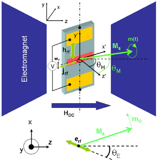
The sample is rotated in the electromagnet with the static magnetic field applied perpendicular (=0∘) to parallel to the film plane (=90∘). We define the sample magnetization: and the current in the ferromagnetic electrode: where is the equilibrium magnetization in static conditions. It makes an angle with the normal to the sample . is the time-varying part of the magnetization. We do not apply any bias current to the system: and consider the RF current created in the ferromagnetic layer by the non-vanishing RF electric field: where is the constant phase difference between the current and the magnetization precession at resonance. The generalized Ohm’s law then writes:Juretschke1960
| (22) |
, and are the resistivity, the anisotropic magnetoresistance and the anomalous Hall constant of the ferromagnetic electrode. Since we experimentally measure a DC voltage, we calculate the time average of :
| (23) |
where: , and . We then obtain the voltage:
| (24) |
where . The first term corresponds to the planar Hall effect and the second one to the anomalous Hall effect. and are then determined by solving the Landau-Lifschitz-Gilbert (LLG) equation:
| (25) |
where is the gyromagnetic ratio, the damping factor and the effective magnetic field given by:
| (26) |
Here we only consider the shape anisotropy field. The radiofrequency magnetic field can be written as: , where =9.4 GHz is the X-band cavity frequency. In static conditions, the magnetization equilibrium angle is found by solving: i.e. . The resolution of the LLG equation yields:
| (27) | |||||
| (28) | |||||
| (29) |
where: , and . By using: , and , we finally find:
| (30) | |||||
| (31) |
where: and . The FMR spectrum is defined by . Then, after time averaging, we obtain:
| (32) | |||||
| (33) |
Here we point out that the rf electric field induces an
additional angular dependence because change with the DC magnetic field angle as
where is the direction
of the rf electric field in the cavity (see Fig. 13). Note that is proportional to the strength of the rf electric field, i.e.
to the strength of the rf magnetic field. As a consequence the magnitude of
the electromotive forces and are
proportional to . Hence they exhibit a linear dependence
with the microwave power as shown in the main text. Such
linear dependence might allow to deduce either the ratio
or the phase shift . Since the Hall
coefficient is of the order of and is
of the order of G, then is much smaller than
the anisotropic magnetoresistance, .
The OOP angular dependence of the symmetric component of either
or clearly shows a behavior different from that
of the ISHE out-of-plane angular dependence () as shown in Fig. 4(c) where we considered
and .
Appendix B Charge backflow into the ferromagnet by the ISHE in Ge
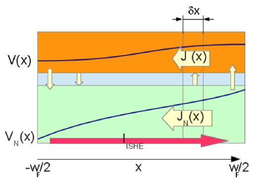
At the ferromagnetic resonance of the CoFeB electrode, the combination of spin pumping and ISHE creates a charge current (in A/m) in the Ge layer. Part of this charge current flows back to the ferromagnetic and tantalum capping layers which affects the estimation of and in germanium. In the following, we make an estimation of this backflow current. In Fig. 14, the current density crossing the interface at corresponds to the variation of the current in the layers:
| (34) | |||
| (35) |
where , and are the thickness, current density and potential in the Ta/CoFeB bilayer; is the resistance-area product of the interface between CoFeB/MgO and Ge. The current densities in each layer with conductivities and can be written:
| (36) | |||
| (37) |
the current conservation involving the current source due to spin pumping and ISHE gives:
| (38) |
which can also be written:
| (39) |
by using the symmetry of the system, we set the origin of in the middle of the trilayer and find:
| (40) |
| (41) |
which gives the following solution:
| (42) |
with:
| (43) |
| (44) | |||
| (45) |
The current in the Ta/CoFeB bilayer (proportional to the derivative of ) vanishes at the edges () which gives access to the constant :
| (46) |
Then the ratio between the induced voltage in Ge and the current is given by:
| (47) |
where: . (resp. ) is the thickness (resp. conductivity) of the tantalum capping layer.
References
- (1) I. Zutic, J. Fabian, and S. Das Sarma, Rev. Mod. Phys. 76, 323 (2004).
- (2) D. D. Awschalom and M. E. Flatté, Nature Phys. 3, 153 (2007).
- (3) I. Zutic and H. Dery, Nature Mater. 10, 647 (2011).
- (4) S. P. Dash, S. Sharma, R. S. Patel, M. P. de Jong, and R. Jansen, Nature 462, 491 (2009).
- (5) B. T. Jonker, G. Kioseoglou, A. T. Hanbicki, C. H. Li, and P. E. Thompson, Nature Phys. 3, 542 (2007).
- (6) I. Appelbaum, B. Huang, and D. J. Monsma, Nature 447, 295 (2007).
- (7) T. Suzuki, T. Sasaki, T. Oikawa, M. Shiraishi, Y. Suzuki, and K. Noguchi, Appl. Phys. Exp. 4, 023003 (2011).
- (8) Y. Zhou, W. Han, L.-T. Chang, F. Xiu, M. Wang, M. Oehme, I. A. Fischer, J. Schulze, R. K. Kawakami, and K. L. Wang, Phys. Rev. B 84, 125323 (2011).
- (9) A. Jain, L. Louahadj, J. Peiro, J. C. Le Breton, C. Vergnaud, A. Barski, C. Beigné, L. Notin, A. Marty, V. Baltz, S. Auffret, E. Augendre, H. Jaffrès, J. M. George, and M. Jamet, Appl. Phys. Lett. 99, 162102 (2011).
- (10) H. Saito, S. Watanabe, Y. Mineno, S. Sharma, R. Jansen, S. Yuasa, K. Ando, Solid State Comm. 151, 1159 (2011).
- (11) K.-R. Jeon, B.-C. Min, Y.-H. Jo, H.-S. Lee, I.-J. Shin, C.-Y. Park, S.-Y. Park, and S.-C. Shin, Phys. Rev. B 84, 165315 (2011).
- (12) A. T. Hanbicki, S.-F. Cheng, R. Goswami, O. M. J. van’t Erve and B. T. Jonker, Solid State Comm. 152, 244 (2012).
- (13) A. Fert and H. Jaffrès, Phys. Rev. B 64, 184420 (2001).
- (14) M. Tran, H. Jaffrès, C. Deranlot, J.-M. George, A. Fert, A. Miard, and A. Lemaître, Phys. Rev. Lett. 102, 036601 (2009).
- (15) S. P. Dash, S. Sharma, J. C. Le Breton, J. Peiro, H. Jaffrès, J.-M. George, A. Lemaître, and R. Jansen, Phys. Rev. B 84, 054410 (2011).
- (16) M. Cantoni, D. Petti, C. Rinaldi, and R. Bertacco, Appl. Phys. Lett. 98, 032104 (2011).
- (17) D. Lee, S. Raghunathan, R. J. Wilson, D. E. Nikonov, K. Saraswat, and S. X. Wang, Appl. Phys. Lett. 96, 052514 (2010).
- (18) Y. Zhou, W. Han, Y. Wang, F. Xiu, J. Zou, R. K. Kawakami, and K. L. Wang, Appl. Phys. Lett. 96, 102103 (2010).
- (19) C. H. Li, O. M. J. van’t Erve, and B. T. Jonker, Nature Comm. 2, 245 (2011).
- (20) A. Jain, J.-C. Rojas-Sanchez, M. Cubukcu, J. Peiro, J. C. Le Breton, E. Prestat, C. Vergnaud, L. Louahadj, C. Portemont, C. Ducruet, V. Baltz, A. Barski, P. Bayle-Guillemaud, L. Vila, J.-P. Attané, E. Augendre, G. Desfonds, S. Gambarelli, H. Jaffrès, J.-M. George, and M. Jamet, Phys. Rev. Lett. 109, 106603 (2012).
- (21) C. Deguet, J. Dechamp, C. Morales, A.-M. Charvet, L. Clavelier, V. Loup, J.-M. Hart- mann, N. Kernevez, Y. Campidelli, F. Allibert, C. Richtarch, T. Akatesu and F. Letertre, Electrochem. Soc. Proc. 2005-06, 78 (2005).
- (22) A. Jain, J.-C. Rojas-Sanchez, M. Cubukcu, J. Peiro, J.-C. Le Breton, C. Vergnaud, A. Augendre, L. Vila, J.-P. Attané, S. Gambarelli, H. Jaffrès, J.-M. George and M. Jamet, Eur. Phys. J. B 86, 140 (2013).
- (23) L. Vila, T. Kimura, and Y. C. Otani, Phys. Rev. Lett. 99, 226604 (2007).
- (24) S. O. Valenzuela and M. Tinkham, Nature 442, 176 (2006).
- (25) M. Morota, Y. Niimi, K. Ohnishi, D. H. Wei, T. Tanaka, H. Kontani, T. Kimura, and Y. Otani, Phys. Rev. B 83, 174405 (2011).
- (26) K. Ando, S. Takahashi, J. Ieda, Y. Kajiwara, H. Nakayama, T. Yoshino, K. Harii, Y. Fujikawa, M. Matsuo, S. Maekawa, and E. Saitoh, J. Appl. Phys. 109, 103913 (2011).
- (27) O. Mosendz, V. Vlaminck, J. E. Pearson, F. Y. Fradin, G. E. W. Bauer, S. D. Bader, and A. Hoffmann, Phys. Rev. B 82, 214403 (2010).
- (28) A. Azevedo, L. H. Vilela-Leão, R. L. Rodriguez-Suárez, A. F. Lacerda Santos, and S. M. Rezende, Phys. Rev. B 83, 144402 (2011).
- (29) L. Liu, T. Moriyama, D.C. Ralph and R.A. Buhrman, Phys. Rev. Lett. 106, 036601 (2011).
- (30) E. Shikoh, K. Ando, K. Kubo, E. Saitoh, T. Shinjo, and M. Shiraishi, Phys. Rev. Lett. 110, 127201 (2013).
- (31) M. Harder, Z. X. Cao, Y. S. Gui, X. L. Fan and C. M. Hu, Phys. Rev. B 84, 054423 (2011).
- (32) Y. Tserkovnyak, A. Brataas, G. E. W. Bauer, and B. I. Halperin, Rev. Mod. Phys. 77, 1375 (2005).
- (33) J. Smit and H.G. Beljers, Philips Res. Rep. 10, 113 (1955).
- (34) B. Heinrich, J. F. Cochran and R. Hasegawa, J. Appl. Phys. 57, 3690 (1985).
- (35) Y. V. Goryunov, N. N. Garif’yanov, G. G. Khaliullin, and I. A. Garifullin, L. R. Tagirov, F. Schreiber, Th. Muhge, and H. Zabel, Phys. Rev. B 52, 13450 (1995).
- (36) W. X. Wang, Y. Yang, H. Naganuma, Y. Ando, R. C. Yu and X. F. Han, Appl. Phys. Lett. 99, 012502 (2011).
- (37) X. Liu, W. Zhang, M. J. Carter and G. Xiao, J. Appl. Phys. 110, 033910 (2011).
- (38) Y. S. Chen, C.-W. Cheng, G. Chern, W. F. Wu and J. G. Lin, J. Appl. Phys. 111, 07C101 (2012).
- (39) Y. Yang, W. X. Wang, Y. Yao, H. F. Liu, H. naganuma, T. S. Sakul, X. F. Han and R. C. Yu, Appl. Phys. Lett. 101, 012406 (2012).
- (40) K. Ando, S. Takahashi, J. Ieda, H. Kurebayashi, T. Trypiniotis, C. H. W. Barnes, S. Maekawa and E. Saitoh, Nature Mater. 10, 655 (2011).
- (41) K. Ando and E. Saitoh, Nature Comm. 3:629 doi: 10.1038/ncomms 1640 (2012).
- (42) L. Liu, C.-F. Pai, Y. Li, H.W. Tseng, D. C. Ralph and R.A. Burhman, Science 336, 555 (2012).
- (43) J.-C. Le Breton, S. Sharma, H. Saito, S. Yuasa and R. Jansen, Nature 475, 82 (2012).
- (44) A. Jain, C. Vergnaud, J. Peiro, J. C. Le Breton, E. Prestat, L. Louahadj, C. Portemont, C. Ducruet, V. Baltz, A. Marty, A. Barski, P. Bayle-Guillemaud, L. Vila, J.-P. Attané, E. Augendre, H. Jaffrès, J.-M. George, and M. Jamet, Appl. Phys. Lett. 101, 022402 (2012).
- (45) K.-R. Jeon, B.-C. Min, J.-Y. Park, K.-D. Lee, H.-S. Song, Y.-H. Park, Y.-H. Jo and S.-C. Shin, Scientific Rep. 2, 962 (2012).
- (46) Y. Tserkovnyak, A. Brataas, and G.E.W. Bauer, Phys. Rev. Lett. 88, 117601 (2002).
- (47) E. I. Rashba, Phys. Rev. B 62, R16267 (2000).
- (48) G. Schmidt, D. Ferrand, L. W. Molenkamp, A. T. Filip, and B. J. van Wees, Phys. Rev. B 62, R4790 (2000).
- (49) A. Brataas, G.E.W. Bauer and P. J. Kelly, 427, 157-255 (2006).
- (50) H. Jiao, and G.E.W. Bauer, arXiv:1210.0724v1 [cond-mat.mes-hall] (2012).
- (51) V. Castel, N. Vliestra, J. Ben Youssef, and B. J. van Wees, Appl. Phys. Lett. 101, 132414 (2012).
- (52) A. I. Larkin and K. A. Matveev, Zh. Eksp. Teor. Fiz. 93, 1030 (1987) [Sov. Phys. JETP 66, 580 (1988)].
- (53) H. J. Juretschke, J. Appl. Phys. 31, 1401 (1960).