Weak localization scattering lengths in epitaxial, and CVD graphene
Abstract
Weak localization in graphene is studied as a function of carrier density in the range from 1 x cm-2 to 1.43 x cm-2 using devices produced by epitaxial growth onto SiC and CVD growth on thin metal film. The magnetic field dependent weak localization is found to be well fitted by theory, which is then used to analyse the dependence of the scattering lengths Lφ, Li, and L∗ on carrier density. We find no significant carrier dependence for Lφ, a weak decrease for Li with increasing carrier density just beyond a large standard error, and a n dependence for L∗. We demonstrate that currents as low as 0.01 nA are required in smaller devices to avoid hot-electron artefacts in measurements of the quantum corrections to conductivity.
pacs:
73.43.Qt, 72.80.Vp, 72.10.DiI Introduction
In recent years graphene has proved of great interest both for its huge range of potential applications, from enhancing the strength of composite materialsStankovich et al. (2006), to high-speed analogue electronicsBourzac (2012); and for its impressive range of physical properties, including an anomalous integer quantum Hall effectNovoselov et al. (2005), quantized opacityNair et al. (2008), and its two-dimensionalityNovoselov et al. (2005). Amongst other properties it shows a greatly enhanced weak (anti)localization effectNovoselov et al. (2005), which is the principal topic of this paper.
The nature of weak (anti)localization in graphene has attracted a significant amount of controversyGeim and Novoselov (2007). It was originally predicted that the effect would be entirely of the weak antilocalization type due to the existence of a Berry phase in graphene. Early results, however, failed to show such behaviourGeim and Novoselov (2007). Subsequently, it was realized that this could be resolved by the addition of further scattering terms which break chirality, particularly elastic intervalley scatteringMcCann et al. (2006).
The purpose of this paper is the fitting of scattering lengths using the theory of McCann et al.McCann et al. (2006) for a wide range of different graphene samples. The fittings are used to demonstrate the validity of this method for devices with carrier densities ranging from 1 x cm-2 to 1.43 x cm-2. Devices are analysed from graphene produced by epitaxial growth on SiCJanssen et al. (2011), and chemical vapour deposition (CVD) onto thin metal filmsChen et al. (2012). The results are compared with those obtained from the literatureLara-Avila et al. (2011a); Tikhonenko et al. (2008a); Ki et al. (2008); Jauregui et al. (2011) and together are used to measure trends in the scattering lengths with carrier density.
II Methodology and Theoretical Background
Hall bar devices were produced using graphene derived from the epitaxial and CVD fabrication methods. The devices were produced using e-beam lithography and oxygen plasma etching. The epitaxial graphene was grown on the Si-terminated face of SiCJanssen et al. (2011), with contacts made using large area titanium-gold contacting. Photochemical gating was used to control the carrier density on the epitaxial devices due to the impossibility of conventional backgating through SiCLara-Avila et al. (2011b). CVD graphene was grown on thin-film copper, subsequently transferred to Si/SiO2, and contacts were made using chrome-gold tracks/bondpads followed by gold-only final contacting, as described in our previous workBaker et al. (2012a). Various sizes of large-area Hall bar were produced; dimensions were typically 64 x 16 m2 for the CVD devices, and 160 x 35 m2 for the epitaxial devices. Considerable care was taken to record the magnetotransport data with the use of slow magnetic field sweep rates passing completely through the zero field resistance peak. Measurements of the phase of Shubnikov-deHaas and Quantum Hall effect oscillations at higher fieldsBaker et al. (2013) demonstrate that all samples studied were monolayer graphene with charge density fluctuations less than the measured carrier density.
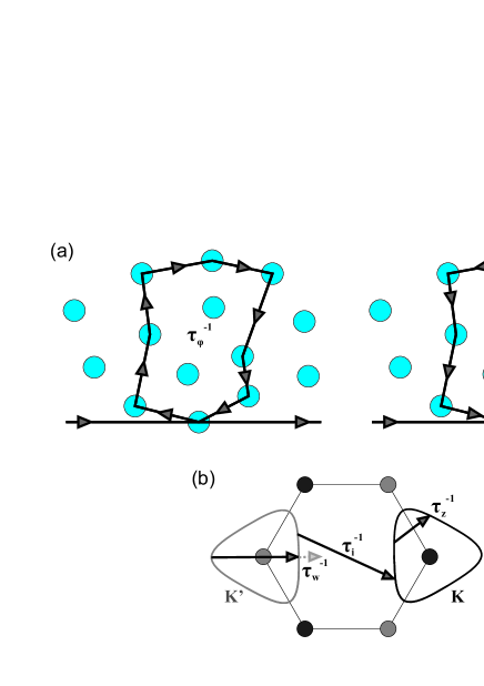
Weak (anti)localization is a quantum interference effect which occurs at low temperatures when electrons retain phase coherenceCastro Neto et al. (2009). Fig. 1 shows four scattering terms which contribute to this process. Fig. 1 (a) shows , the dephasing rate due to inelastic scatteringMcCann et al. (2006). Fig. 1 (b) shows the three other main scattering termsTikhonenko et al. (2008b): , the elastic intervalley scattering rate which comes from atomically sharp scatterers and scattering from the edges of the device, , the elastic intravalley trigonal warping scattering term, and finally , the elastic intravalley chirality breaking scattering term which comes from dislocations or other topological defects. These processes are grouped together as a single originally definedMcCann et al. (2006) as . (The alternative definition of is not used here).
Fig. 1 (a) displays two self-intersecting scattering paths. These two paths are identical except for the direction of travel around the loop. Interference between such loops is the origin of the weak (anti)localization effect. If these paths constructively interfere, such loops are more common than would be expected classically, resulting in an increase in resistance known as weak localization. The converse, the destructive interference case, is called weak antilocalization. Due to the need to maintain phase coherence for an interference effect to occur, acts to control the localization through the maximum size of such loops which is given by the decoherence length defined by where D, the diffusion coefficient = , is the Fermi velocity, which is 1.1 x 10⁶ms-1 as measured in both epitaxial SiC/GMiller et al. (2009) and exfoliated material Deacon et al. (2007) and is the transport scattering time as determined from the carrier mobility. Hence controls the magnitude of the weak (anti)localization effect.
Whether we are operating in a weak localization regime, or a weak antilocalization regime, depends on the phase the carriers pick up while traversing such a path. Because of the existence of a Berry phase in monolayer grapheneNovoselov et al. (2005), the two trajectories are expected to gain a phase difference of , leading to destructive interference, and hence weak antilocalizationHorsell et al. (2008). However, in the presence of significant elastic intervalley scattering (), weak localization can be restored. The reason for this is that chirality is reversed between the two valleysFal’ko et al. (2007); hence trajectories involving intervalley scattering allow for zero phase difference between two self-intersecting paths which leads to constructive interference and hence weak localization.
The weak (anti)localization effect can be destroyed by increasing either the magnetic field or temperature to a sufficient value. Increased magnetic fields add a random relative phase to the carriers as they traverse curved paths, causing the interference effect to be averaged awayCastro Neto et al. (2009). Increased temperature has the effect of decreasing , which reduces the magnitude of both types of localization effect, as can be seen from Eq. (2).
This paper makes use of the main result from McCann et al.McCann et al. (2006) to produce fits of the resistivity as a function of magnetic field, B, to the measured weak (anti)localization,
| (1) | |||||
where , is the digamma function and . At small magnetic fields, where , we can approximate . Using this we can simplify Eq. (1) for small fields as,
| (2) | |||||
From this equation it is clear how variations in control the magnitude of the weak (anti)localization. It is also clear how significant intervalley scattering, , is required to produce a positive resistivity correction, i.e. weak localization. In practice, significant intervalley scattering is found in most samples, and therefore, weak localization is far more commonly found than weak antilocalizationTikhonenko et al. (2009).
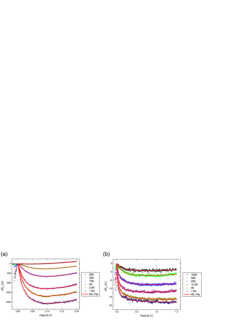
Fig. 2 shows data from the extremes of carrier density of the measured samples. The samples are found to be very well fitted by the McCann theoryMcCann et al. (2006), despite the two samples having very different magnitudes, shape, and field range for the localization. To attain the best possible fits care must be taken to avoid landing in local minima of the parameter space, especially when and/or are very short.
III Scattering Lengths
Fitting to the magnetoresistivity as shown in Fig. 2 for 8 different samples with carrier densities from 1 x cm-2 to 1.4 x cm-2 allows us to extract the scattering times using Eq. (1) and these were converted to scattering lengths using, . Fig. 3 shows the extracted scattering lengths, from our data and from the literatureLara-Avila et al. (2011a); Tikhonenko et al. (2008a); Ki et al. (2008); Jauregui et al. (2011). Care was taken to extract all values for as close as possible to the same temperature, in this case 1.5 K. This is done since Lφ in particular is known to vary strongly with temperatureLara-Avila et al. (2011a); Tikhonenko et al. (2008a); Ki et al. (2008); Jauregui et al. (2011). Fits to the data are made using a simple power law, , the results of which are shown in Table 1.
To within the standard error we find no variation with carrier density for the phase coherence length (Lφ) despite the very different physical nature of the epitaxial, exfoliated and CVD samples. Previous work has typically found similar values for Lφ of around 0.6 mLara-Avila et al. (2011a); Tikhonenko et al. (2008a); Ki et al. (2008); Jauregui et al. (2011). In Ki et al.Ki et al. (2008), there has been some previous work carried out on the carrier density dependence by using a single sample with a backgate. In their work they found a superlinear increase of Lφ with carrier density. These devices, however, were very small at 6 x 1 m2 and were probably effected by boundary scattering. More indirectly, temperature studies have also been carried out on Lφ, the modelling of which could in principle be used to predict a carrier density dependence. In Ki et al.Ki et al. (2008), the behaviour of the scattering length is modelled using two electron-electron interaction terms, a direct Coulomb term and a Nyquist scattering term. These terms do have a carrier density dependence, however, the fitting parameters were found to vary with carrier density. Lara-Avila et al.Lara-Avila et al. (2011a) use an alternative model and find their data to be well modelled by the addition of a electron spin-flip scattering term. This is due to scattering from the localized magnetic moment of spin-carrying defects which is likely to be dependent on the sample preparation method and could mask or dominate underlying trends in the dependence of the phase coherence length on carrier density.
| Scattering | Exponent | Exponent | Multiplicative |
|---|---|---|---|
| Length | (A) | Standard Error | Constant (B) |
| Lφ | 3.59 m | ||
| Li | 2.25 m | ||
| L∗ | 4.47 m |
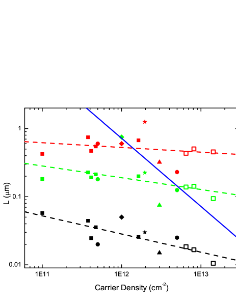
For the elastic intervalley scattering term, Li, we find a weak trend with carrier density with a negative exponent of -0.173. Previous temperatureLara-Avila et al. (2011a); Ki et al. (2008) and backgate studiesKi et al. (2008) found no strong variation of Li with either temperature or carrier density. Given that Li is due to short range, atomically sharp scatterers and device-edge scattering, it would be expected to be highly dependent on the device characteristics. We might also expect that there would be some correlation with the the ungated carrier density as this is related to the number of defects through shifting of the Fermi level by the presence of charged defectsKatoch et al. (2010). In particular, for the data presented here, the highest ungated carrier densities are found for CVD graphene devices which are associated with high levels of polycrystallinity. This implies a large number of atomically sharp scatterers, and hence could account for the lower values of Li measured at high carrier densities using CVD samples.
The strongest trend, with an exponent of -0.267, and smallest standard error () is found for , the sum of all the sublattice-symmetry-breaking perturbations. For all samples in Fig. 3, Li L∗ and hence L∗ will be predominantly made up from Lw, the elastic intravalley trigonal warping scattering term, and Lz, which allows for other chirality breaking elastic intravalley processes. We would expect the trigonal warping term to increase with carrier density, since the degree of trigonal warping is dependent on the Fermi energyMcCann et al. (2006). The Lz term is expected to be relatively independent of carrier density due to its origin from topological defectsTikhonenko et al. (2008b). McCann et al.McCann et al. (2006) produce the following prediction of how is expected to vary with carrier density,
| (3) |
where , the structure constant , is the nearest neighbour overlap integral, is the lattice constant, EF is the Fermi energy, and is the Fermi velocity. This equation predicts that Lw should be proportional to , and is shown in Fig. 3 as a solid blue line suggesting that the trigonal warping term will not become dominant until around 1 x cm-2. For the region studied we find a much slower variation with n of approx n suggesting that Lz is dominant and only varies weakly with carrier density.
IV Maximum Currents
In this section the importance of using sufficiently low currents is demonstrated, together with how the use of too large currents may explain the observations of a “saturation” in Lφ sometimes found in the literature. Because of the very large optical phonon energies in grapheneYan et al. (2007), the dominant cooling mechanism for carriers at low temperatures comes from acoustic phononsBaker et al. (2012a). The acoustic phonon cooling in graphene is a fairly weak mechanism which allows carriers to attain temperatures far in excess of that of the latticeBaker et al. (2012a, 2013), and at low temperatures in the Bloch-Grüneisen limit this process is strongly temperature dependent. This “hot-carrier” effect can be described using the theory of KubakaddiKubakaddi (2009), which has been shown experimentally to predict the energy loss rates very accuratelyBaker et al. (2012a, 2013). Using this theory, we can calculate the effective minimum carrier temperature, Te,min, that can be obtained for a given device for each current. Kubakaddi presents the relation for the energy loss rate per carrier,
| (4) |
where Te is the carrier temperature, and TL is the lattice temperature. For a given current and sample resistance Rxx, this can be equated to the power input per carrier from the current as
| (5) |
where n is the carrier density, and A is the sample area. The coefficient is calculated using the relation
| (6) |
where is the Riemann zeta function, is the sample density, and is the sound velocity. This can be rearranged to give the effective minimum carrier temperature,
| (7) |
Using the numerical values suggested by KubakaddiKubakaddi (2009) we calculate = 5.36 x W K-4 / , where n is in units of 1012 cm-2.
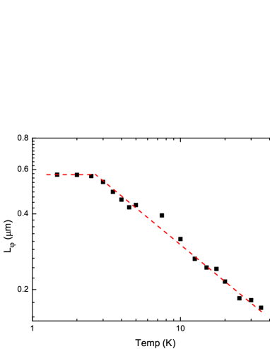
Fig. 4 shows data from one of our epitaxial samples which exhibits a saturation in the measured value of Lφ with decreasing temperature. The sample has a carrier density of 4.72 x cm-2, a size of 160 x 35 m2 and a sample resistance of 8.2 k. All the data for the graph was collected with a current of 500 nA. Using Eq. (7) we calculate Te,min for the sample as 1.97 K. This value corresponds well to the temperature of the measured onset of the saturation regime presented in the figure.
When previously encountered, this saturation in measured Lφ at quite high temperatures has been attributed variously to magnetic impuritiesKi et al. (2008), electron-hole puddles reducing the effective conducting areaKi et al. (2008), and limits imposed directly from the sample sizeTikhonenko et al. (2008a). We believe the above hot-carrier effects should also be taken into account, particularly when the sample size is physically small. Giving further weight to the validity of the hot-carrier explanation, Lara-Avila et al.Lara-Avila et al. (2011a) showed that significant changes in Lφ could still be observed at temperatures below 100 mK by using a large area device and a current of 50 pA for which Eq. (7) predicts Te 20 mK. Further evidence for electron temperature saturation in graphene has been observed recently through measurements of bolometric response in noise powerFong and Schwab (2012),Betz et al. and resistivity Yan et al. (2012) which require similar energy loss rates to those used hereKubakaddi (2009); Baker et al. (2012a, 2013).
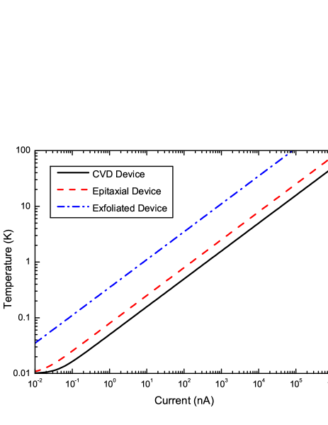
By way of illustration we calculate the currents required to achieve a given carrier temperature for three different examples of typical samples used here and in the literature which we present in Fig. 5. The epitaxial device in the figure is the one from Fig. 4, the CVD device is the one from Fig. 2 (b), and the third, exfoliated graphene device is a typical device similar to many of those used in the literature of dimensions 5 x 1 m2. It is striking, and worth emphasizing, that for this device to attain a carrier temperature of 30 mK, it requires maximum currents of 0.01 nA.
V Conclusions
Using the theory of McCann et al.McCann et al. (2006) we have shown that high quality fits to weak-localization can be obtained for devices with carrier densities from 1 x cm-2 to 1.43 x cm-2 for graphene fabricated by both the epitaxial and CVD methods. We have investigated carrier density dependences for Lφ, Li, and L∗. We find no evidence of a significant density dependence for Lφ and only a weak decrease in Li with increasing density, though this may be due to a coincidental increase in disorder. Finally, we find evidence of a weak power law decrease in L∗ with a carrier density dependence of approximately n. We have also shown that hot electron effects may obscure the true temperature dependence of the scattering lengths unless currents as low as 0.01 nA are used for measurements at dilution fridge temperatures in small devices.
VI Acknowledgements
This work was supported by the UK EPSRC, Swedish Research Council and Foundation for Strategic Research, UK National Measurement Office, and EU FP7 STREP ConceptGraphene.
References
- Stankovich et al. (2006) S. Stankovich, D. a. Dikin, G. H. B. Dommett, K. M. Kohlhaas, E. J. Zimney, E. a. Stach, R. D. Piner, S. T. Nguyen, and R. S. Ruoff, Nature 442, 282 (2006), ISSN 1476-4687.
- Bourzac (2012) K. Bourzac, Nature 483, S34 (2012).
- Novoselov et al. (2005) K. S. Novoselov, A. K. Geim, S. V. Morozov, D. Jiang, M. I. Katsnelson, I. V. Grigorieva, S. V. Dubonos, and A. A. Firsov, Nature 438, 197 (2005), ISSN 1476-4687.
- Nair et al. (2008) R. R. Nair, P. Blake, A. N. Grigorenko, K. S. Novoselov, T. J. Booth, T. Stauber, N. M. R. Peres, and A. K. Geim, Science 320, 1308 (2008).
- Geim and Novoselov (2007) A. K. Geim and K. S. Novoselov, Nat. Mater. 6, 183 (2007), ISSN 1476-1122.
- McCann et al. (2006) E. McCann, K. Kechedzhi, V. I. Fal’ko, H. Suzuura, T. Ando, and B. L. Altshuler, Phys. Rev. Lett. 97, 146805 (2006).
- Janssen et al. (2011) T. J. B. M. Janssen, A. Tzalenchuk, R. Yakimova, S. Kubatkin, S. Lara-Avila, S. Kopylov, and V. I. Fal’ko, Phys. Rev. B. 83, 233402 (2011), ISSN 1098-0121.
- Chen et al. (2012) C.-H. Chen, C.-T. Lin, Y.-H. Lee, K.-K. Liu, C.-Y. Su, W. Zhang, and L.-J. Li, Small 8, 43 (2012), ISSN 1613-6829.
- Lara-Avila et al. (2011a) S. Lara-Avila, A. Tzalenchuk, S. Kubatkin, R. Yakimova, T. J. B. M. Janssen, K. Cedergren, T. Bergsten, and V. Fal’ko, Phys. Rev. Lett. 107, 166602 (2011a).
- Tikhonenko et al. (2008a) F. V. Tikhonenko, D. W. Horsell, R. V. Gorbachev, and A. K. Savchenko, Phys. Rev. Lett. 100, 056802 (2008a), ISSN 0031-9007.
- Ki et al. (2008) D. K. Ki, D. Jeong, J. H. Choi, H. J. Lee, and K. S. Park, Phys. Rev. B. 78, 125409 (2008).
- Jauregui et al. (2011) L. a. Jauregui, H. Cao, W. Wu, Q. Yu, and Y. P. Chen, Solid State Commun. 151, 1100 (2011), ISSN 00381098.
- Baker et al. (2012a) A. M. R. Baker, J. A. Alexander-Webber, T. Altebaeumer, and R. J. Nicholas, Physical Review B 85, 115403 (2012a).
- Baker et al. (2013) A. M. R. Baker, J. A. Alexander-Webber, T. Altebaeumer, S. D. McMullan, T. J. B. M. Janssen, A. Tzalenchuk, S. Lara-Avila, S. Kubatkin, R. Yakimova, C.-T. Lin, et al., Phys. Rev. B 87, 045414 (2013).
- Lara-Avila et al. (2011b) S. Lara-Avila, K. Moth-Poulsen, R. Yakimova, T. Bjø rnholm, V. Fal’ko, A. Tzalenchuk, and S. Kubatkin, Adv. Mater. 23, 878 (2011b), ISSN 1521-4095.
- Castro Neto et al. (2009) A. H. Castro Neto, F. Guinea, N. M. R. Peres, K. S. Novoselov, and A. K. Geim, Rev. Mod. Phys. 81, 109 (2009).
- Tikhonenko et al. (2008b) F. Tikhonenko, D. Horsell, B. Wilkinson, R. Gorbachev, and A. K. Savchenko, Physica E 40, 1364 (2008b), ISSN 13869477.
- Miller et al. (2009) D. L. Miller, K. D. Kubista, G. M. Rutter, M. Ruan, W. A. de Heer, P. N. First, and J. A. Stroscio, Science 324, 924 (2009).
- Deacon et al. (2007) R. S. Deacon, K.-C. Chuang, R. J. Nicholas, K. S. Novoselov, and A. K. Geim, Phys. Rev. B. 76, 081406 (2007), ISSN 1098-0121.
- Horsell et al. (2008) D. W. Horsell, F. V. Tikhonenko, R. V. Gorbachev, and A. K. Savchenko, Phil. Trans. R. Soc. A 366, 245 (2008), ISSN 1364-503X.
- Fal’ko et al. (2007) V. I. Fal’ko, K. Kechedzhi, E. McCann, B. Altshuler, H. Suzuura, and T. Ando, Solid State Commun. 143, 33 (2007), ISSN 00381098.
- Tikhonenko et al. (2009) F. V. Tikhonenko, A. A. Kozikov, A. K. Savchenko, and R. V. Gorbachev, Phys. Rev. Lett. 103, 226801 (2009), ISSN 0031-9007.
- Katoch et al. (2010) J. Katoch, J.-H. Chen, R. Tsuchikawa, C. W Smith, E. R Mucciolo, and M. Ishigami, Phys. Rev. B. 82, 081417 (2010).
- Yan et al. (2007) J. Yan, Y. Zhang, P. Kim, and A. Pinczuk, Phys. Rev. Lett. 98, 166802 (2007), ISSN 0031-9007.
- Kubakaddi (2009) S. S. Kubakaddi, Physical Review B 79, 075417 (2009).
- Fong and Schwab (2012) K. C. Fong and K. C. Schwab, Phys. Rev. X. 2, 031006 (2012).
- (27) A. C. Betz, F. Vialla, D. Brunel, C. Voisin, M. Picher, A. Cavanna, A. Madouri, G. F ve, J.-M. Berroir, B. Pla ais, et al., Phys. Rev. Lett. 109, 056805 (2012).
- Yan et al. (2012) J. Yan, M.-H. Kim, J. A. Elle, A. B. Sushkov, G. S. Jenkins, H. M. Milchberg, M. S. Fuhrer, and H. D. Drew, Nat. Nanotechnol. 7, 472 (2012).