Enhanced and continuous electrostatic carrier doping on the SrTiO3 surface.
Abstract
Paraelectrical tuning of a charge carrier density as high as 1013 cm-2 in the presence of a high electronic carrier mobility on the delicate surfaces of correlated oxides, is a key to the technological breakthrough of a field effect transistor (FET) utilising the metal-nonmetal transition. Here we introduce the Parylene-C/Ta2O5 hybrid gate insulator and fabricate FET devices on single-crystalline SrTiO3, which has been regarded as a bedrock material for oxide electronics. The gate insulator accumulates up to 1013cm-2 carriers, while the field-effect mobility is kept at 10 cm2/Vs even at room temperature. Further to the exceptional performance of our devices, the enhanced compatibility of high carrier density and high mobility revealed the mechanism for the long standing puzzle of the distribution of electrostatically doped carriers on the surface of SrTiO3. Namely, the formation and continuous evolution of field domains and current filaments.
Introduction
A prominent feature of phase transitions in correlated electron systems is the nanoscale dynamics leading to future electronics such as switching devices and novel nonvolatile resistance-change memory applications chakhalian ; hwang ; hormoz ; inoue1 ; xiang ; asanuma ; nakano ; zyang ; yang . In spite of the long-standing research, device prototypes remain limited mainly due to the absence of a method for a continuous (i.e., paraelectrical) and precise electrostatic control (gating) of a two dimensional (2D) charge carrier density 1013 cm-2. Furthermore, oxygen and cation stoichiometry are fairly unstable in perovskite-type (ABO3) transition-metal oxides (TMOs) phillips . Deposition of dielectric oxides on the surface of ABO3 channel for gating inevitably results in such kind of defects, introducing randomness and eventually smearing the critical features of metal-insulator transitions miyashita . In the face of these challenges, we have chosen to fabricate FET adopting single-crystalline SrTiO3 for the channel.

This compound is a band insulator with a crystal structure characteristic of many TMO Mott insulators, and becomes metallic by electron doping. SrTiO3 is an n-type wide-gap semiconductor with a band gap of 3.2eV. It is considered as a matrix for spintronic devices due to the unique configuration of the spin-precession vector at the surface and the absence of the Dresselhaus term nakamura2012 . The surface of the single crystal can be atomically flat and is widely used as a substrate for correlated TMO thin films, making it preferable candidate to test the suitability of the reported gate insulator for future electronics. Identifying the technical methods and physical mechanism for paraelectric tuning of electronic conduction in two dimensional electron gases (2DEG) created at the surface of SrTiO3 is a problem of bursting interdisciplinary interest dagotto .
High-density charge accumulation cm-2 was recently realised yuan through an electric double-layer (EDL) on the surface of electrolytes such as ionic liquids. Although the gating with EDL is a promising method for future correlated electron devices, its viability is hindered, because ionic liquids on the surface of TMOs may trigger redox reactions, causing vacancies at the interface especially in the presence of high electric fields ueno2010-1 ; ueno2010-2 . In addition, the continuous control of the carrier density with EDL can be done only by using liquid electrolytes, which are unsuitable for integration to the present solid-state electronics.
| Sample | Amount of raw material (mg) | Bilayer capacitance per area (nF/cm2) | Estimated Parylene-C thickness (nm) |
|---|---|---|---|
| A | 300 | 34 | 57.7 |
| B | 350 | 24.97 | 87.9 |
| C | 400 | 22.25 | 101.7 |
| D | 600 | 12.56 | 199.9 |
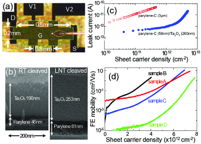
Here, we have engineered a bilayer of poly-monochloro-para-xylylene (known as Parylene-C) gorham with Ta2O5, Fig. 1. Ta2O5 has a high dielectric constant = 25 and a relatively high dielectric strength 4 MV/cm sethi . The combination of Ta2O5 and Parylene-C into a single gate insulator enabled a sheet carrier density of 1013 cm-2 while keeping the field effect mobility of the SrTiO3 surface at 10 cm2/Vs. Fabrication details can be found in the Methods Summary. The electronic transport measurements were performed using an Agilent 4155C semiconductor parameter analyser.
Results
Fig. 1 (c) shows the gate leak currents plotted against the sheet carrier density for the bilayer gate insulator and for the single Parylene-C gate insulator. Although the total thickness of the bilayer gate insulator is 10 times thinner than the 3 m-thick Parylene-C, the leak current of the bilayer is an order of magnitude lower, which is similar to the trend reported earlier deman . Hence, the sputtering deposition of Ta2O5 does not damage the Parylene-C thin film. Fig. 1 (d) depicts an upturn in the increase of the field effect mobility at sheet carrier densities cm-2. The field effect mobility is defined as , where is the sheet conductance and is the nominal sheet carrier density in the channel region. is the channel current, (and ) is the distance (and voltage difference) between channel electrodes V2 and V1, is the channel width, is the measured total capacitance per unit area, and is the elementary charge. Although increased almost exponentially with the application of , the - behaviour is different from that in the conventional subthreshold regime. In fact, all our samples showed extremely large , 10 cm2/Vs at large carrier densities (i.e., large ) without reaching saturation even at room temperature. Thus, we set the threshold voltage = 0. Notably, is an order of magnitude larger than earlier reports for a Parylene-C/SrTiO3 FET at room temperature ( = 0.3 cm2/Vs for = 31012 cm-2) nakamura3 , and comparable to the bulk Hall mobility of SrTiO3 ahrens .
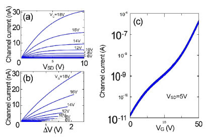
The typical - characteristics of Sample B in Fig. 2 (a) indicate that the current saturates for large as in conventional semiconductor FETs, where it occurs due to the pinch-off of the channel. The saturation vanishes when the channel current in Fig. 2 (a) is plotted against the voltage drop inside the channel , Fig. 2 (b). Hence, the pinch-off region is rather small even at low and emerges between the drain and the V2 electrode for below 5 V. Fig. 2 (c) shows that the current increases monotonically from 1 nA to 100 A as the gate voltage increases up to 40 V, thereby demonstrating a continuous electrostatic control of the sheet carrier density.

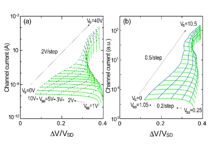
Furthermore, for small fixed values of , although the channel current does not change very much (Fig. 3 (a)), the ratio decreases rapidly with increasing . This feature can be associated with the formation of field domains ridley . We also observe that in various parameter conditions, approaches the geometrical value 0.37 = (V1-V2 distance 295m)/(source-drain distance 800 m). This indicates that in those regimes the contact resistance between SrTiO3 and Al electrodes, which is expected to be ohmic, is indeed negligibly small compared to the channel resistance of SrTiO3. It is interesting, however, to observe the behaviour of with increasing and with fixed (small) value of in Fig. 3 (a). This feature is the so-called S-type negative differential resistivity (SNDR) associated with the formation of current filaments ridley .

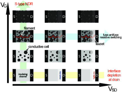
The rather complicated behaviour of the vs curves in Fig. 3 (a) was qualitatively reproduced (Fig. 3 (b)) by a model calculation based on the following assumptions: (i) the existence of a low regime where charge carriers are mainly spatially and inhomogeneously confined in cells, and move through the channel region by incoherent tunnelling, (ii) a higher regime where the conductive cells overlap and percolating conduction paths are formed, and (iii) a well developed homogeneous 2DEG with barriers formed at the interfaces. We modelled the experimental system through a 2D resistor network array where the transport properties of each cell is determined primarily by the local electron density. The cells are assumed to be randomly distributed shallow potential wells for carriers with a site dependent potential strength . At low and , the cells have low density and the carriers are confined. The carriers move between cells by a variable range hopping (VRH) mechanism. At higher applied voltages, the occupation of cells increases and the carriers delocalise, augmenting their mobility. For given external potentials and , we solve for the resistor network and compute the local voltages at all cells along the 2D channel. These local voltages are then compared to the corresponding values of the local confining potential of the cell . If their difference is negative, the mobility is assumed to be the VRH type, whereas if it is positive, we adopt a much larger value, consistent with a band-like conduction in the metallic state. The interfaces at the source and drain electrodes are simply modelled as barriers with potential height . The details of the model and the numerical study are presented in the Supplementary Materials. Our numerical study captures the qualitative transport behaviour shown in Fig. 3, providing new insight to the conduction states of 2DEGs in SrTiO3. In fact, it demonstrates that the system evolves through a variety of regimes connected through crossovers depicted schematically in Fig. 4.
Discussion
In summary, we have demonstrated that the Parylene-C/Ta2O5 bilayer overcomes previous limitations, achieving the required large electrostatic carrier doping, while keeping a high quality interface with the TMO. The hybrid gate insulator can sustain a sheet carrier density of 81012 cm-2, without introducing formidable damage to the channel interface, as the field-effect mobility of SrTiO3 exceeds 10 cm2/Vs, even at room temperature. The excellent agreement of our numerical study with measurements on the hybrid gate insulator, indicate a continuous evolution through a variety of different regimes, including tuneability of field domains and current filaments on the surface of SrTiO3. Our findings provide a novel method for paraelectrical tuning of metal-nonmetal transitions in correlated electron devices made of ABO3-type TMOs. Notably, the fabrication details and physical mechanism reported here may be applied towards emergent oxide electronics controlled by low dimensional charge carrier transport.

Further to the practical interest, low temperature studies on similar devices would reveal whether granular superconductivity beloborodov in SrTiO3 could be realised for small and . Indeed, the behaviour of possible superconducting cells with dimensions comparable to characteristic length scales may be considerably different from bulk materials. Moreover, the quantum confinement in the cells may lift the degeneracy of the lowest energy band of SrTiO3, affecting the Rashba effect on its surface nakamura2012 .
METHODS SUMMARY
Preparation of Parylene-C thin film was performed as follows. In a ϕ46 mm quartz tube, di-monochloro-para-xylylene was sublimated at 150 , the dimer flew into a high temperature (800 ) region williams , where it was cleaved into two monomer units gorham . The reactive intermediates were then transported to a room temperature deposition chamber at the pressure of 210-4 Pa. Upon condensation on the surface of single-crystalline SrTiO3, spontaneous polymerisation into Parylene-C took place. The Parylene-C thin film deposited through this so-called Gorham methodgorham provides excellent conformal coating on the SrTiO3 surface. The thin film of Ta2O5 was deposited directly on the top of the Parylene-C by radio frequency (rf) sputtering at room temperature. We used a Ta2O5 ceramic target in a flowing Ar gas of 25 sccm and 5.5 Pa. The rf power was 2 W/inch2, and the sample-target distance was 140 mm. The thickness of the Ta2O5 layer was 200 nm measured by a surface profiler (KLA Tencor). On the top of Ta2O5, a 150 nm thick Au gate electrode with a 5 nm Ti adhesion layer was deposited by electron-beam deposition. The thickness of the Parylene-C layer was estimated from the measured capacitance of a built-in capacitor (of area 800 800 m2), using the known values = 3.2 for Parylene-C, and = 25 for Ta2O5.
We used the Al metal for source and drain electrodes; Al gives ohmic contact to SrTiO3. For the other parts of the device fabrication process, we followed the same method and used the same materials as reported by Nakamura et al. nakamura1
For some samples, the thickness of the gate insulator was also measured by an S-4800 (Hitachi High-Tech) scanning electron microscope (SEM); the values were in good agreement with those estimated from the capacitance. Since the Parylene-C is much softer than Ta2O5, when we tried to expose the cross sections for the SEM measurement, either cutting with a scalpel or simply cleaving, the bilayer at room temperature easily deformed (stretches and shrinks at the ends) the Parylene-C layer, and the fibrils of Parylene-C always extended out of the cross section. We found that freezing the samples in liquid N2 facilitates the cleaving.
Fig. 1 (b) shows the comparison of the cross section of a sample cleaved at room-temperature and one at liquid-N2 temperature. The Parylene-C cross section in the latter case appears rather lumpy. However, this was never observed in the cross sections of the samples cleaved at room-temperature; thus, it is likely that the uneven cross section is due to the steep rise of temperature with heavy bedewing in air after the cleavage in liquid-N2. It has been shown that a conventionally deposited planar Parylene-C thin film gorham does not possess nanostructured morphology damirel .
Acknowledgements
We are grateful to H. Shima, T. Yamada and T. Hasegawa for technical help. This work was supported by the Japan-Singapore Joint-Research Program, the Japan Society for the Promotion of Science (JSPS) and the National Research Foundation, Singapore through Competitive Research Programme (CRP Award No. NRF-CRP-4-2008-04). I.H.I. was partly supported by Grants-in-Aid for Scientific Research (category A, grant number 24244062).
Author Contributions
I.H.I. and C.P. conceived and supervised the project. A.B.E. fabricated the devices and performed all the measurements. I.H.I. contributed to the experimental setup. P.S. and M.J.R. did the numerical simulation study. All the authors discussed the results and co-wrote the manuscript. Correspondence and requests for materials should be addressed to I.H.I. (i.inoue@aist.go.jp) or C.P. (christos@ntu.edu.sg).
Additional Information
Supplementary Information accompanies this paper at www.nature.com.
References
- (1) Chakhalian, J., Millis, A. J. & Rondinelli, J. Whither the oxide interface. Nat. Mater. 11, 92-94 (2012).
- (2) Hwang, H. Y. et al. Emergent phenomena at oxide interfaces. Nat. Mater. 11, 103-113 (2012).
- (3) Hormoz, S. & Ramanathan, S. Limits on vanadium oxide Mott metal-insulator transition field-effect transistors. Solid-State Electr. 54, 654-659 (2010).
- (4) Inoue, I. H. Electrostatic carrier doping to perovskite transition-metal oxides. Semicond. Sci. Technol. 20, S112-S120 (2005).
- (5) Xiang, P. -H. et al. Strain-mediated phase control and electrolyte-gating of electron-doped manganites. Adv. Mat. 23, 5822-5827 (2011).
- (6) Asanuma, S. et al. Tuning of the metal-insulator transition in electrolyte-gated NdNiO3 thin films. App. Phys. Lett. 97, 142110 (2010).
- (7) Nakano, M. et al. Collective bulk carrier delocalization driven by electrostatic surface charge accumulation. Nature 487, 459-462 (2012).
- (8) Yang, Z., Ko, C. & Ramanathan, S. Oxide electronics utilizing ultrafast metal-insulator transitions. Ann. Rev. Mater. Res. 41, 337-367 (2011).
- (9) Yang, J. J., Inoue, I. H., Mikolajick, T. & Hwang, C. S. Metal oxide memories based on thermochemical and valence change mechanisms. MRS Bull. 37, 131-137 (2012).
- (10) Phillips, J. C. Physics of complex metals — temperature-dependent resistivities in ionic superconductors and stable quasi-crystals. Phys. Rev. B 46, 8542-8558 (1992).
- (11) Miyashita, S. Phase transition in spin systems with various types of fluctuations. Proc. Jpn. Acad., Ser. B 86, 643-666 (2010).
- (12) Dagotto, E. The conducting face of an insulator. Nature 469, 167-168 (2011).
- (13) Yuan, H. et al. High-density carrier accumulation in ZnO field-effect transistors gated by electric double layers of Ionic Liquids. Adv. Funct. Mater., 19, 1046-1053 (2009).
- (14) Ueno, K. et al. Electric-field-induced superconductivity in an insulator. Nature Mater. 7, 855-858 (2008).
- (15) Ueno, K., Shimotani, H., Iwasa, Y. & Kawasaki, M. Electrostatic charge accumulation versus electrochemical doping in SrTiO3 electric double layer transistors. Appl. Phys. Lett. 96, 252107 (2010).
- (16) Gorham, W. F. A new general synthetic method for preparation of linear poly-p-xylylenes. J. Polym. Sci. A-1 4, 3027-3039 (1966).
- (17) Sethi, G. et al. Structure and Dielectric Properties of Amorphous Tantalum Pentoxide Thin Film Capacitors. 2007 Annual Report Conference on Electrical Insulation and Dielectric Phenomena, 815-818 (2007).
- (18) Deman, A.-L. & Tardy, J. PMMA-Ta2O5 bilayer gate dielectric for low operating voltage organic FETs. Org. Electron. 6, 78-84 (2005).
- (19) Nakamura, H. Electrostatic carrier density control in SrTiO3. D. Eng. Thesis, University of Tokyo, 2006.
- (20) Ahrens, M., Merkle, R., Rahmati, B. & Maier, J. Effective masses of electrons in n-type SrTiO3 determined from low-temperature specific heat capacities. Physica B 393, 239-248 (2007).
- (21) Ridley, B. K. Specific negative resistance in solids. Proc. Phys. Soc. 82, 954-966 (1963).
- (22) Beloborodov, I. S., Lopatin, A. V., Vinokur, V. M. & Efetov, K. B. Granular electronic systems. Rev. Mod. Phys. 79, 469-518 (2007).
- (23) Nakamura, H., Koga, T. & Kimura, T. Experimental evidence of cubic Rashba effect in an inversion-symmetric oxide. Phys. Rev. Lett. 108, 206601 (2012).
- (24) Williams, J. M. & Rowen, J. T. Diagnosis and therapy for a recalcitrant parylene coater. J. Vac. Sci. Technol. A 5, 2760-2762 (1987).
- (25) Nakamura, H. et al. Low temperature metallic state induced by electrostatic carrier doping of SrTiO3. Appl. Phys. Lett. 89, 133504 (2006).
- (26) Demirel, M. C. Emergent properties of spatially organized poly(p-xylylene) films fabricated by vapor deposition. Col. Surf. A 321, 121-124 (2008).
- (27) Inoue, I. H., Yasuda, S., Akinaga, H. & Takagi, H. Nonpolar resistance switching of metal/binary-transition-metal oxides/metal sandwiches: Homogeneous/inhomogeneous transition of current distribution. Phys. Rev. B 77, 035105 (2008).