The Equilibrium Shape of Graphene Domains on Ni(111)
Abstract
We have determined the equilibrium shape of graphene domains grown on Ni(111) via carbon segregation at 925C. In situ, spatially-resolved electron diffraction measurements were used to determine the crystallographic orientation of the edges of the graphene domains. In contrast to recent theoretical predictions of a nearly-circular shape, we show that graphene domains, which nucleate with random shapes, all evolve toward a triangular equilibrium shape with ‘zig zag’ edges. Only one of the two possible zig-zag edge orientations is observed.
In many technological applications, large, defect-free graphene domains are required in order to achieve high performance. Understanding the thermodynamics and kinetics of graphene growth – especially at metal surfaces – is consequently of great interest. However, measuring the properties of graphene domains during growth is difficult due to the elevated substrate temperature and harsh growth conditions. Here we describe in situ measurements of the equilibrium shape of graphene domains grown on Ni(111) at 925C. Our approach makes use of a novel imaging mode that enables electron diffraction information to be obtained from specific surface features during real-space imaging.
There have been several studies of the influence of growth conditions on the shape of graphene domains. For example, on Ni(111), Olle et al. showed that either hexagonal or triangular graphene domain shapes can be controllably synthesized under suitable conditions Olle et al. (2012). On Cu(111), Chen et al. observed triangular domains (with zig-zag edges) formed using ferrocene-dicarboxylic acid as a carbon source Chen et al. (2012), whereas conventional, high-temperature CVD growth using methane yields hexagonal domains with zig-zag edges Yu et al. (2011). Clearly, growth kinetics can play an important role in determining the graphene domain shape.
Here we focus on the equilibrium shape of graphene domains on Ni. Ni(111) is a particularly interesting substrate because graphene growth is epitaxial. As we show, the epitaxial relationship strongly influences the thermodynamics of graphene domains. Specifically, we find that graphene domains, which nucleate with random shapes, evolve toward triangular shapes that exhibit only one type of zig-zag edge. This is in contrast to the hexagonal shape found for free-standing graphene Girit et al. (2009); Gan and Srolovitz (2010) as well as for graphene grown on (111) oriented Cu foilsYu et al. (2011). The observed triangular equilibrium shape is also in contradiction with a recent first-principles study Artyukhov et al. (2012). In that work the energy difference between the zig-zag and arm-chair orientations on Ni(111) was found to be small, and a smooth, rounded equilibrium shape was predicted not .
In our experiments, graphene was grown on both crystalline Ni(111) foils and epitaxial Ni(111) films. The films consisted of 100 nm of Ni sputter deposited onto annealed C-plane sapphire. The foils were grown via electrodeposition Shin et al. (2007), with thicknesses in the range 10 - 20 m. Clean Ni(111) surfaces were prepared by in situ sputtering with 1 keV Ne ions, followed by annealing at 900C. Surface contamination was monitored using x-ray photoelectron spectroscopy.
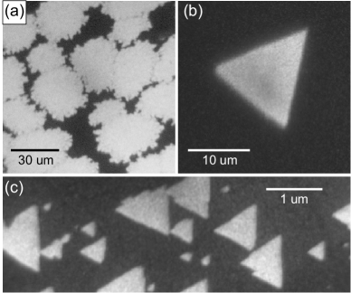
Graphene can be grown on Ni in two ways: direct CVD growth from the vapor, and by segregation of carbon from the Ni bulk to the surface. In our experiments, Graphene was first grown by exposing the surface to Torr of ethylene at a substrate temperature of 850C. During ethylene exposure, the surface was imaged using photoelectron emission spectroscopy (PEEM). When graphene nucleation was observed, the ethylene pressure was reduced. Because of the relatively high growth rate, the domain shape was irregular and clearly not equilibrated, as shown in Fig. 1a. Better control of the graphene growth rate was achieved using cycles of dissolution and segregation. Upon heating to 990C, graphene domains dissolve as carbon migrates to the bulk due to increased carbon solubility at elevated temperature. When the temperature is lowered (e.g. to 925 C) graphene domains reform as carbon segregates to the surface as shown in Fig. 1b,c.
The growth rate during segregation can be controlled by adjusting the substrate temperature, and can be directly monitored using LEEM. If the growth rate is low, large triangular domains are observed, despite the fact that a typical domain crosses many tens of steps (the average terrace width is roughly nm). This shows that atomic-height surface steps do not strongly influence the shape of the domains. However, when the surface morphology is significantly disrupted, e.g. at twin boundaries or at large step bunches, the domain boundary can be influenced by the local surface morphology.
To equilibrate the domain shapes, we used in situ LEEM imaging, and the ability to precisely control the growth rate, to ‘anneal’ the domains at essentially constant area. We grew isolated domains at a low growth rate (0.2 m2/s) until the areas reached roughly 1 m2. The temperature was then increased slightly so that the domains ceased to grow. The shapes were then observed for an extended period of time. We found that the domains all adopted polygonal shapes with edges normal to (Fig. 1c). Over time, the domains evolved towards a simple triangular shape (Fig. 1b), indicating that this shape is the equilibrium geometry.
The graphene domains exhibit a diffraction pattern in spatially-resolved LEED. The diffraction pattern indicates that the graphene is epitaxial, as expected, but does not directly reveal the orientation of the domain edge. To determine the crystallographic orientation of the substrate, the diffraction pattern must be oriented with respect to the real-space image. To do this we exploit the spherical aberration of the cathode lens system to generate a ‘real-space’ diffraction pattern.
Due to diffraction at the sample surface, the incident electron beam in LEEM generates diffracted beams, in addition to the specularly-reflected beam. These beams emerge from the sample at specific angles defined by the diffraction condition. In a perfect imaging system (free of spherical aberration) the images formed from the different beams will coincide in the image plane. However in LEEM the spherical aberration of the cathode lens is large, and the images arising from different diffracted beams do not perfectly coincide, but are displaced with respect to each other in manner that reflects the crystal structure and symmetry. In fact, measuring the relative positions of these images can be used to determine the spherical aberration coefficient Tromp (2013).
Here we use the real-space diffraction pattern formed by the displaced images to determine the orientation of the graphene domains with respect to the Ni reciprocal lattice, and hence the crystallographic orientation of the domain edge.

An image of an isolated domain is shown in Fig. 2a. Real-space diffraction images were recorded using a small aperture (1 m diameter) to illuminate specific regions of the surface near the domain. The areas illuminated by the incident beam are indicated by ovals in Fig. 2a, and the corresponding real-space diffraction patterns are shown in Fig. 2b. In the Fig. 2b, each diffracted beam produces a 1m image of the illuminated area. When the Ni is illuminated, the pattern is clearly three-fold symmetric. When the graphene domain is illuminated, the pattern is still three-fold symmetric, but all six first-order diffraction spots are visible. Comparison with the domain shape (shown as a red outline) shows that the domain edges are perpendicular to the reciprocal lattice vectors of the substrate. This, in turn, shows that the graphene edges are parallel to the ‘zig-zag’ orientation (normal to ).
For free-standing graphene, or graphene on incommensurate substrates including Cu(111), the six possible zig-zag orientations are equivalent, and the equilibrium shape is hexagonal. However, because graphene on Ni(111) is epitaxial, there are two inequivalent zig-zag orientations as shown in Fig. 2c, which are labeled and . The local environments of the carbon edge atoms are very different in the and structures, at least for the un-relaxed, un-reconstructed structures shown in Fig. 2c. The edge atoms in are located over fcc hollow sites, whereas the edge atoms in the are located directly on top of substrate Ni atoms.
To determine which type of edge is observed in experiment (i.e. or ), the intensities of the diffracted spots must be considered. The six first-order diffraction spots are not equivalent. As shown in Fig. 2b (top panel), for diffraction from Ni(111) at 47 eV, three spots are bright and three are very dim. The intensities of the diffracted beams are determined by the positions of the Ni atoms within the unit cell, and can be computed for various crystal structures Pendry (1974).
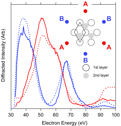
The dashed lines in Fig. 3 show the calculated diffracted intensity for the and beams as a function of the incident electron energy Sun et al. (2010). The calculation shows that for an energy of 40 eV, the diffraction spots will be significantly more intense than the spots. At 50 eV, the situation is reversed, and the spots will be intense. Intensity-versus-voltage (or ‘IV’) curves measured in this work are shown as solid lines in Fig. 3 and agree well with calculated intensities (dashed lines).
The orientation of the diffracted beams with respect to the Ni(111) unit cell is indicated in the inset to Fig. 3. This information can be used to determine the orientation of the crystal in Fig. 2. The diffraction patterns from Ni(111) shown in Fig. 2b (top and bottom panels) were recorded at 47 eV, and therefore the bright spots are the diffracted beams of Fig. 3. The corresponding crystal orientation is shown in Fig. 2c. Once the crystal orientation is determined, it is clear that the observed domain shape has the -type zig-zag structure.
The favorability of the -type edge is, perhaps, puzzling. In the unrelaxed structure, the carbon edge atoms are located over fcc hollow sites. In contrast, the edge atoms in the -structure are located directly over Ni atoms, and presumably interact strongly with the Ni substrate. Furthermore, the triangular shape contradicts the expectation of a compact, rounded domain shape based on recent first-principles calculations Artyukhov et al. (2012). In that work, Artyukhov et al. considered a number of edge terminations for graphene domains on several metal surfaces. For Ni(111), the formation energies of the zig-zag edge and reconstructed arm-chair edge (A5’) were found to be roughly 0.4 eV/Å. A reconstructed version of the zig-zag edge (Z57) was found to have considerably higher energy than the unreconstructed zig-zag structures shown in Fig. 2c. The similarity of the edge energies suggests a nearly circular equilibrium shape, especially at elevated temperature. One explanation for the clear stability of the -type zig-zag orientation that we observe is that the edge structure is more complicated than the structures considered by Artyukhov et al.. Specifically, those authors only considered reconstructions that involved a rearrangement of the carbon atoms at the edge. Given the significant interaction between graphene and Ni, as well as the high mobility of Ni atoms during graphene growth, it may be that the equilibrium edge structure incorporates Ni. To test this hypothesis we computed the formation energies of several edge structures that incorporate excess Ni.
The calculations were carried out by using the Vienna ab initio simulation package (VASP),Kresse and Furthmüller (1996) with exchange-correlation functional described by Ceperley-Alder local density approximation (LDA)Ceperley and Alder (1980) and interaction between core electrons and valence electrons by the frozen-core projector-augmented wave (PAW) method.Blöchl (1994) An energy cutoff of 415 eV was used for the plane wave basis expansion. The Ni(111) substrate was modeled by slabs of four atomic layers. A vacuum region of more than 12 Å was used to prevent the interaction between periodic slabs. During the structural relaxation, the Ni atoms of bottom two layers were fixed in their bulk position. All other atoms were allowed to relax until the force on each atom was smaller than 0.02 eV/Å. A 1121 -point scheme was used to sample reciprocal space.
Graphene ribbons with a width of Å were used to compute the edge energies. The ribbon supports and -type edges on opposite sides. We find that the zig-zag edge formation energy, e.g. , is 0.36 eV/Å, in good agreement with Artyukhov et al. Artyukhov et al. (2012). We considered a number of -type edge terminations that involve more complex Ni-C edge structures, including: (1) Ni adatoms at the graphene edge, and (2) Ni atoms substituted for C edge atoms. None of the structures we considered has a lower formation energy than the unreconstructed zig-zag structures shown in Fig. 2c. Structures with Ni substituted for C are particularly unfavorable. It is possible that the actual structure is more complicated than the ones we considered. In addition, the elevated growth temperature could be an important factor. The calculations correspond to zero temperature, and it may be that entropy plays a significant role in stabilizing a Ni-decorated structure at the growth temperature (925C). That is, the equilibrium shape at high temperature could be very different from that at low temperature.
In summary, we have used a novel real space diffraction measurement technique to determine the orientation of equilibrated graphene domains on Ni(111). At 925C, the random domain shapes observed after nucleation evolve towards a triangular shape with the -type zig-zag edges. The fact that the -type orientation is favored is in contraction with first-principles calculations that suggest that the energy difference between zig-zag and arm-chair orientations is small. It may be that triangular shape we observe is stabilized by a more complex C-Ni edge structure, which could explain the apparent discrepancy with earlier theoretical work.
References
- Olle et al. (2012) M. Olle, G. Ceballos, D. Serrate, and P. Gambardella, Nano Lett. 12, 4431 (2012).
- Chen et al. (2012) X. Chen, S. Liu, L. Liu, X. Liu, X. Liu, and L. Wang, Appl. Phys. Lett. 100, 163106 (2012).
- Yu et al. (2011) Q. Yu, L. A. Jauregui, W. Wu, R. Colby, J. Tian, Z. Su, H. Cao, Z. Liu, D. Pandey, D. Wei, T. F. Chung, P. Peng, N. P. Guisinger, E. A. Stach, J. Bao, S.-S. Pei, and Y. P. Chen, Nat. Mater. 10, 443 (2011).
- Girit et al. (2009) Ç. Ö. Girit, J. C. Meyer, R. Erni, M. D. Rossell, C. Kisielowski, L. Yang, C.-H. Park, M. F. Crommie, M. L. Cohen, S. G. Louie, and A. Zettl, Science 323, 1705 (2009).
- Gan and Srolovitz (2010) C. K. Gan and D. J. Srolovitz, Phys. Rev. B 81, 125445 (2010).
- Artyukhov et al. (2012) V. I. Artyukhov, Y. Liu, and B. I. Yakobson, P. Natl. Acad. SCI. USA 109, 15136 (2012).
- (7) The authors find that the lowest energy armchair orientation is actually reconstructed.
- Shin et al. (2007) J. W. Shin, A. Standley, and E. Chason, Appl. Phys. Lett. 90, 261909 (2007).
- Tromp (2013) R. Tromp, Ultramicroscopy in press, (2013).
- Pendry (1974) J. B. Pendry, Low Energy Electron Diffraction (Academic Press, London, 1974).
- Sun et al. (2010) J. Sun, J. B. Hannon, R. M. Tromp, P. Johari, A. A. Bol, V. B. Shenoy, and K. Pohl, ACS Nano 4, 7073 (2010).
- Kresse and Furthmüller (1996) G. Kresse and J. Furthmüller, Phys. Rev. B 54, 11169 (1996).
- Ceperley and Alder (1980) D. M. Ceperley and B. J. Alder, Phys. Rev. Lett. 45, 566 (1980).
- Blöchl (1994) P. E. Blöchl, Phys. Rev. B 50, 17953 (1994).