e-mail: sach@isp.kiev.ua††thanks: 41, Prosp. Nauky, Kyiv 03680, Ukraine\sanitize@url\@AF@joine-mail: sach@isp.kiev.ua††thanks: 41, Prosp. Nauky, Kyiv 03680, Ukraine\sanitize@url\@AF@joine-mail: sach@isp.kiev.ua††thanks: 41, Prosp. Nauky, Kyiv 03680, Ukraine\sanitize@url\@AF@joine-mail: sach@isp.kiev.ua††thanks: 41, Prosp. Nauky, Kyiv 03680, Ukraine\sanitize@url\@AF@joine-mail: sach@isp.kiev.ua††thanks: 41, Prosp. Nauky, Kyiv 03680, Ukraine\sanitize@url\@AF@joine-mail: sach@isp.kiev.ua
INFLUENCE OF SURFACE CENTERS
ON THE EFFECTIVE SURFACE
RECOMBINATION RATE AND
THE PARAMETERS OF SILICON SOLAR CELLS
Abstract
The results of our researches of the influence of exponentially distributed surface centers on the effective surface recombination rate and the parameters of silicon solar cells (SCs) are reported. In our calculations, we assumed the acceptor and donor surface states to lie in the upper and lower, respectively, parts of the bandgap. The model also supposed a discrete surface level to exist in the middle of the energy gap. In the case where the integrated concentration of continuously distributed centers is comparable with that of deep surface levels, those centers can affect the SC parameters only due to the recombination. If the concentration of continuously distributed centers is comparable or higher than the concentration characterizing a charge built-in into the insulator, those centers directly affect the surface band bending and the photo-induced electromotive force. With the help of a computer simulation, the conditions for the rate of surface recombination through continuously distributed surface centers to exceed that through the deep discrete level are determined. A decrease of the open-circuit voltage in inverted silicon SCs associated with the recombination through continuously distributed centers is calculated. The obtained theoretical results are compared with the experimental data.
1 Introduction
Nowadays, researchers deal with a quite considerable number of semiconductor interfaces, the properties of which are substantially governed by surface electron states. Such objects include, in particular, the interface between a semiconductor and an insulator. The charge characteristics of those interfaces have been studied more completely than the recombination ones. While studying the former, it was found that the acceptor surface states are located, as a rule, in the upper part of the energy gap and the donor surface states in the lower one. Depending on the energy, the surface states with either a peak-like distribution or with the exponential dependence of their density on the energy–the so-called continuously distributed surface states–can be realized. Information concerning the charge characteristics of the Si–SiO2 interface was summarized, e.g., in monograph [1]. In particular, it was shown in work [1] that the consideration of the exponential distribution of surface centers in the silicon bandgap into account allows one to explain the experimental results obtained, while studying the generation parameters of silicon-based metal–insulator–semiconductor structures.
As to the mechanism of surface recombination formation, it is supposed in modern works on this subject that a discrete surface level located near the middle of the energy gap makes a crucial contribution to the recombination. The same can be said about works devoted to the analysis of the surface recombination in solar cells on the basis of single-crystalline silicon (see, e.g., works [2, 3], in which either silicon dioxide or aluminum oxide was used to reduce the surface recombination rate).
Researches of such promising versions of silicon solar cells as elements with rear-side metallization have been activated recently [4, 5, 6]. In those elements, the task to minimize the rate of surface recombination on the illuminated surface is extremely challenging.
This work is aimed at analyzing the relation between the contributions made to the surface recombination by surface levels located near to and far from the middle of the energy gap, as well as its dependence on the Fermi level position at the surface. It is shown that, under certain conditions, the contribution of remote surface levels to the recombination can substantially exceed the deep-level contribution. The influence of exponentially distributed surface states on the open-circuit voltage and the short circuit current in silicon-based solar cells has been analyzed.
2 Formulation of the Problem
According to work [1], let us consider the Si–SiO2 interface and suppose that the acceptor surface levels are located in the upper half of the silicon energy gap, the donor surface levels are in the lower half, and their concentrations exponentially grow, while approaching the corresponding band edges; in addition, there is a discrete surface level near the energy gap middle-point. Let us analyze their contributions to the surface recombination taking into account that their cross-sections and, accordingly, the coefficients of electron and hole capture change with the energy, as was described in work [1]. More specifically, the cross-section of the hole capture by acceptor states grows, whereas the same parameter for electrons decreases, as the distance from the middle of the energy gap increases, with the energy dependence for the cross-sections being steeper than that for the center concentration. For donor levels located in the lower half of the energy gap, the cross-sections of the electron capture grow, whereas those of the hole capture decrease. For the sake of simplicity, let the system of centers be symmetric. In the middle of the energy gap, there is a discrete surface level with concentration . In addition, the concentrations of donor and acceptor centers per unit energy interval and the coefficients of electron and hole capture by continuously arranged surface levels behave themselves as follows:
| (1) |
Here, and are the concentrations of donor and acceptor centers, respectively, per unit energy interval at the energy-gap middle point; is the capture factor at ; and and are the characteristic energies of variations in the concentration and the capture cross-section, respectively.
From the electroneutrality equation for the system with regard for the recharging of surface levels at the illumination, the dimensionless nonequilibrium band bending can be determined. Let us include the charge built-in into the insulator, in the electroneutrality equation. Then, in the case of an -semiconductor, the equation looks like
| (2) |
In this expression for donor and acceptor centers,
is the nonequilibrium Fermi distribution for the surface level with energy and the capture factors and for electrons and holes, respectively; and are the equilibrium concentrations of electrons and holes, respectively, in the bulk; and and are the same quantities, but at the semiconductor surface. We also use the following notation: is the concentration of charge carriers in the intrinsic semiconductor, the energy gap width in the semiconductor, the Debye screening length, the bulk concentration of completely ionized donors, the thickness of the space charge region (SCR) in the semiconductor, the Boltzmann constant, and the temperature. The energy is reckoned from the middle of the energy gap at the semiconductor surface.
In order to find a relation between the surface and bulk concentrations of nonequilibrium charge carriers, let us use the approximation of constant Fermi quasilevels for electrons and holes in the SCR. In this case, for the injection level ,
| (3) |
| (4) |
In Fig. 1, the theoretical dependences of the surface photovoltage (in millivolt units) on the injection level calculated with the use of Eqs. (1)–(4) are depicted. The calculations were carried out for , and the varied calculation parameter was the concentration of exponentially distributed surface levels (it has the dimensionality of /eV). The highest photovoltage values were obtained in the cases (curve 1) and (curve 2). If the integrated concentration of exponentially distributed surface centers is comparable with , the photovoltage magnitude decreases, and the strongest decrease takes place at large enough injection levels (curves 3 and 4). This is a manifestation of the effect when a charge built-in into an insulator is screened by the charge of surface centers.
With regard for Eqs. (3) and (4), the densities of surface recombination fluxes, i.e. the density of recombination currents normalized by the electron charge that flow through the discrete surface level and through the continuously distributed acceptor and donor levels are equal, respectively, to
| (5) |
| (6) |
| (7) |
The surface density of the total recombination flux is determined by the expression
| (8) |
Knowing the recombination fluxes, we can find the effective rates of surface recombination through the corresponding levels,
| (9) |
as well as the total effective rate of surface recombination,
| (10) |
One can see from expressions (5)–(10) that the effective rate of surface recombination through the deep discrete level can be determined using a standard procedure. At the same time, to find the effective rates of surface recombination through continuously distributed centers, it is necessary to integrate the recombination fluxes through the acceptor and donor levels over the energy.
3 Discussion of Results
In Figs. 2 and 3, the dependences of the total effective surface recombination rate and the effective recombination rates of surface recombination through the deep level, , and the acceptor, , and donor, , states on the quantity calculated for the cases and , respectively, are depicted. The following parameters were used at calculations: , cm-2, = cm3/s, , cm3/s, , , and . Note that the values taken for and correspond to those quoted in work [1]. One can see that, for the selected and values, the concentrations of continuously distributed levels grow more slowly than the coefficients of hole capture by acceptor levels and electron capture by donor levels. It should be noted that, at the used and values and , the presence of surface levels weakly affect the magnitude of (see curve 2 in Fig. 1).
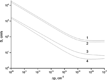
In the case (see Fig. 2), the effective rates of surface recombination through the continuously distributed states are low in comparison with that through the deep surface level. In this case, the dependence of the effective surface recombination rates on the injection level in the recession interval is approximated well by the dependence , which is typical of the recombination in the SCR [7]. In the case where the concentration of continuously distributed levels increases with the energy more rapidly than the cross-sections of electron and hole capture change, i.e. the inequality is obeyed, and the integrated concentrations of continuously distributed levels are comparable with the concentration of deep levels, the rates and dominate.
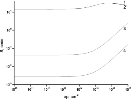
In the case (see Fig. 3), the contribution of continuously distributed donor levels to the surface recombination rate substantially exceeds that of the deep discrete level, and the total surface recombination rate is much higher than the value obtained above, when only the recombination through the deep surface level was taken into account. The dependences of the rates of surface recombination through the deep discrete level and the continuously distributed acceptor levels on the injection level magnitude are typical of those obtained in work [8] in the case of inversion band bending, but the same dependence for the effective surface recombination rate through the continuously distributed donor levels is not. In particular, the quantity does not depend on the injection level firstly; then, it increases a little and, afterward, starts to decrease.
It should be noted that, for the parameter set used while plotting Fig. 3, the integrated concentrations of continuously distributed surface levels are close to that of the deep surface level. At the same time, the effective rate of surface recombination through the donor states considerably exceeds that through the deep level, and the rate of recombination through the acceptor states is much lower than that through the deep level. This can be explained by the fact that, in this case, the Fermi level at the surface is located considerably lower than the middle of the energy gap, and, as a result, the recombination fluxes from the conduction and valence bands onto the donor levels are rather close, although they are considerably different for the deep level and the acceptor states.
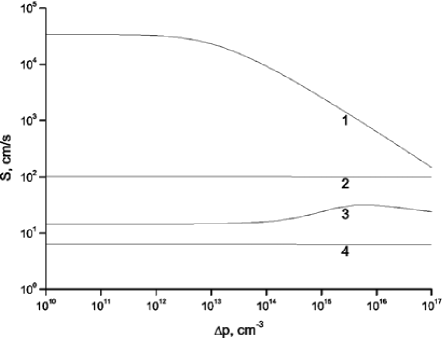
In Fig. 4, the theoretical dependences of the effective surface recombination rates on the injection level are exhibited for the case of a heavily doped semiconductor, when the bulk concentration of electrons amounts to cm-3. In this case, there is a very small depletion band bending at the semiconductor surface, ; and the rate of recombination through the continuously distributed acceptor levels dominates. The latter considerably exceeds the rate of recombination through the deep level at low injection levels, but diminishes as the injection level grows further.
Therefore, if the continuously distributed surface levels can substantially affect the magnitudes of surface band bending and photovoltage, when the integrated concentrations of those states become comparable with , then the effective rates of surface recombination depending on them can considerably exceed the rate of surface recombination through the deep level at much lower integrated concentrations, when they are comparable with the deep level concentration.
The growth of the effective surface recombination rate with results in a reduction of the injection level under open-circuit conditions, which should indirectly affect the voltage in the open circuit, by reducing it. To determine the injection level (the excess concentration) under open-circuit conditions in silicon SCs with the inversion channel, we must solve the equation of balance between generation and recombination. In the case of thin (in comparison with the diffusion length) SCs, this equation looks like
| (11) |
where is the generations flux, the effective surface recombination rate at the illuminated front surface of SC, its value at the rear surface, the SC thickness, and the effective time of bulk recombination with regard for both linear and nonlinear mechanisms of bulk recombination in silicon [4].
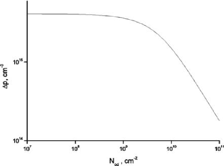
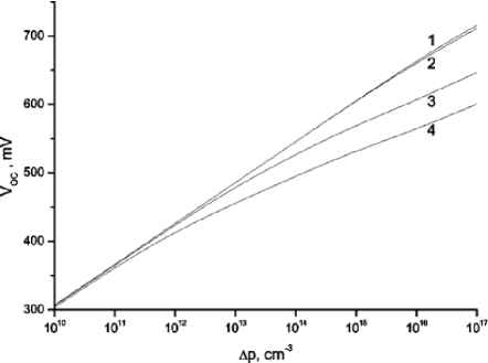
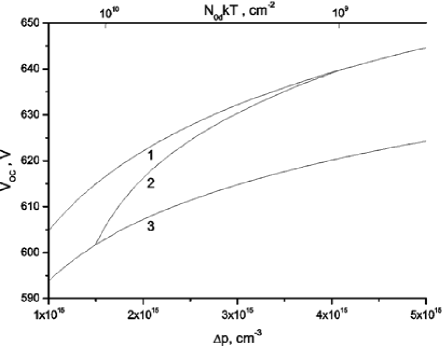
Figures 5 and 6 demonstrate the dependences of magnitude in inverted silicon SCs under AM 1.5 conditions and the open-circuit voltage , respectively, on the concentration of continuously distributed surface centers . The bottom abscissa axis in Fig. 6 serves to indicate the corresponding injection levels. Curve 1 corresponds to the case , curve 3 to the case , and curve 2 was plotted for varying from to . In the latter case, the exponentially distributed surface centers practically do not influence the magnitude of . As one can see from Fig. 6, when the quantity reaches a value of , the magnitude of decreases rather strongly, whereas diminishes by approximately 10%.
In Fig. 7, the dependences of the short-circuit current density in silicon SCs with a metallized rear surface and under AM 1.5 conditions on the concentration of continuously distributed surface centers are shown for the case where there is the conductivity inversion at the SC front surface owing to the charge built-in into the insulator. As one can see from the figure, a reduction of as grows, which is connected with the increase in the effective rate of surface recombination at the front surface, is rather substantial and can reach 17%, provided that the integrated concentration of continuously distributed centers and the concentration of deep levels are equal to each other (at ). Hence, the influence of continuously distributed surface centers on the parameters of inverted silicon SCs owing to both the screening and the enhancement of surface recombination can be strong enough.
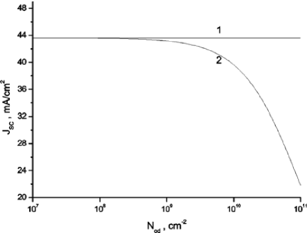
While comparing the results presented in Fig. 7 for the dependence of the short-circuit current density in the SC with the metallized rear surface and the results of numerical 2D simulations described in work [6] (see Fig. 6), it becomes evident that they agree not only qualitatively, but also quantitatively. The matter is that a reduction of the phototransformation efficiency in SCs with rear metallization occurs mainly owing to the growth of the surface recombination rate at the illuminated surface. Using the calculation parameters given in work [5], one can easily get convinced that the increase in the concentration of exponentially distributed donor surface centers within the limits shown in Fig. 7 corresponds to the growth of the surface recombination rate in the interval from 1 to 10 exhibited in Fig. 6 of work [5]. The corresponding reduction in the short-circuit current density completely correlates with the reduction of the phototransformation efficiency in SCs with rear metallization with respect to both the amplitude and the reduction rate.
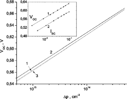
Now, let us estimate the influence of exponentially distributed surface centers in the case of diffusion silicon SCs. As the results shown in Fig. 4 testify, the effective rate of surface recombination in a heavily doped layer substantially increases owing to the continuously distributed acceptor states. In diffusion SCs, this configuration corresponds to the base of the -type. As was shown, e.g., in work [8], the effective surface recombination rate decreases in this case owing to both a stronger doping of the -type region created near the front surface and as a result of its confinement by the rate of charge carrier delivery to the heavily doped layer. The dependences of the open-circuit voltage on the injection level can be calculated with the use of expressions given in work [9]. In Fig. 8, the corresponding plots are exhibited for CSs with the -type base. Curve 1 was plotted with regard for the recombination through the continuously distributed acceptor surface levels, and curve 2 involves only the surface recombination through the deep level located in the middle of the energy gap. Curve 3 is described by the expression
| (12) |
Here, is the factor of CVC non-ideality, and the equilibrium concentration of holes in the base bulk. As one can see from curves 1 and 3, they are in quite a good agreement if and cm-3.
The inset in Fig. 8 demonstrates the experimental dependences for two specimens of diffusion silicon SCs with the base of - or -type. For the SC with the base of -type, the values are larger than those for the SC with the base of -type. The factors of CVC non-ideality for those SCs amount to 1.12 and 1.16, respectively, which is evident from the dependences calculated by the formula
| (13) |
where is the saturation current (curves 1 and 2, respectively). A theoretical fitting showed that, for diffusion SCs with the base of -type, the factor of non-ideality equals 1.12, and the saturation current is . For the specimen with the base of -type, and . If we take into consideration that the saturation current , provided that the rate of surface recombination considerably exceeds that of recombination in the bulk, and put cm/s and cm-3, we obtain .
Let us rewrite expression (12) in the form
Then it becomes evident that dependences (12) and (13) are equivalent in the case and . This means that the theoretical dependence described by curve 2 in Fig. 8 agrees with the experimental dependence for a SC with the base of -type.
Note that the consideration of the surface recombination through continuously distributed surface centers allows not only the theoretical and experimental dependences to be put in agreement, but also the difference of the CVC non-ideality factor from 1 for diffusion SCs at high enough injection levels to be explained.
References
- [1] V.G. Litovchenko and A.P. Gorban’, Fundamentals of Microelectronic Metal–Insulator–Semiconductor Systems (Naukova Dumka, Kyiv, 1978) (in Russian).
- [2] P.P. Altermatt, G. Heiser, X. Dai et al., J. Appl. Phys. 80, 3574 (1996).
- [3] G. Dingemans and W.M.M. Kessels, J. Vac. Sci. Technol. 30, 040802 (2012).
- [4] A.V. Sachenko, A.P. Gorban’, V.P. Kostylev, A.A. Serba, and I.O. Sokolovskii, Fiz. Tekh. Poluprovodn. 41, 1231 (2007).
- [5] O. Nichiporuk, A. Kaminski, M. Lemiti, A. Fave, and V. Skryshevsky, Solar Ener. Mater. Solar Cells 86, 517 (2005).
- [6] O. Nichiporuk, A. Kaminski, M. Lemiti, A. Fave, S. Litvinenko, and V. Skryshevsky, Thin Solid Films 511–512, 248 (2006).
- [7] C.T. Sah, R.N. Noyce, and W. Shockley, Proc. IRE 45, 1228 (1957).
- [8] A.P. Gorban’, V.P. Kostylev, A.V. Sachenko, O.A. Serba, and I.O. Sokolovskii, Ukr. Fiz. Zh. 51, 599 (2006).
-
[9]
A.P. Gorban’, V.P. Kostylev, and A.V. Sachenko, Optoelektron.
Poluprovodn. Tekhn. 34, No.7, 63 (1999).
Received 25.05.12.
Translated from Ukrainian by O.I. Voitenko
В.П. Костильов, А.В. Саченко,
I.О. Соколовський, В.В. Черненко,
Т.В. Слусар, А.В. Суший
ВПЛИВ СИСТЕМИ ПОВЕРХНЕВИХ
ЦЕНТРIВ НА
ЕФЕКТИВНУ ШВИДКIСТЬ
ПОВЕРХНЕВОЇ РЕКОМБIНАЦIЇ
ТА НА ПАРАМЕТРИ
КРЕМНIЄВИХ
СОНЯЧНИХ ЕЛЕМЕНТIВ
Р е з ю м е
В роботi наведено результати
дослiдження впливу рекомбiнацiйних експоненцiально розподiлених
поверхневих центрiв на процеси поверхневої рекомбiнацiї та на
характеристики кремнiєвих сонячних елементiв (СЕ). При розрахунках
вважалося, що система акцепторних поверхневих станiв розташована в
верхнiй половинi забороненої зони кремнiю, а донорних поверхневих
станiв – в нижнiй. Враховувалось також, що бiля середини
забороненої зони знаходиться дискретний поверхневий рiвень.
Показано, що у випадку, коли iнтегральна концентрацiя неперервно
розподiлених центрiв порiвняна з концентрацiєю глибокого
поверхневого рiвня, вони впливають на характеристики кремнiєвих СЕ
лише завдяки рекомбiнацiї. У другому випадку, коли їх концентрацiя
порядку чи бiльша за концентрацiю, яка характеризує вбудований в
дiелектрику заряд, вони безпосередньо впливають на величину
поверхневого вигину зон та на значення фото-ерс. В результатi
комп’ютерного моделювання встановлено умови, за яких швидкiсть
рекомбiнацiї через неперервно розподiленi поверхневi центри бiльша
за швидкiсть рекомбiнацiї через глибокий дискретний рiвень.
Розраховано зменшення напруги розiмкненого кола в кремнiєвих
iнверсiйних СЕ, пов’язане з рекомбiнацiєю через неперервно
розподiленi центри. Розвинуту теорiю порiвняно з експериментом.