Separating the bulk and surface n- to p-type transition in the topological insulator GeBi4-xSbxTe7
Abstract
We identify the multi–layered compound GeBi4Te7 to be a topological insulator with a freestanding Dirac point, slightly above the valence band maximum, using angle–resolved photoemission spectroscopy (ARPES) measurements. The spin polarization satisfies the time reversal symmetry of the surface states, visible in spin–resolved ARPES. For increasing Sb content in GeBi4-xSbxTe7 we observe a transition from n- to p-type in bulk sensitive Seebeck coefficient measurements at a doping of . In surface sensitive ARPES measurements a rigid band shift is observed with Sb doping, accompanied by a movement of the Dirac point towards the Fermi level. Between and the Fermi level crosses the band gap, changing the surface transport regime. This difference of the n- to p-type transition between the surface region and the bulk is caused by band bending effects which are also responsible for a non-coexistence of insulating phases in the bulk and in the near surface region.
pacs:
72.15.Jf, 79.60.Bm, 73.20.AtI Introduction
Since their theoretical prediction and experimental discovery, three–dimensional topological insulators have been established as a new field in solid state physics. In topological insulators a strong spin-orbit coupling is responsible for spin–polarized surface states with a Dirac dispersion in the bulk band gap, forming a conductive surface.Kane and Mele (2005); Hasan and Kane (2010); Qi and Zhang (2011) For experimental devices investigating the transport properties of this kind of material, samples with the Fermi level inside the band gap are of special interest to access the surface states directly. The method of choice to achieve this condition is to tune the Fermi level of a known topological insulator by doping.Zhang et al. (2011); Souma et al. (2012); Arakane et al. (2012) Currently the most popular measurement method in these experiments is angle-resolved photoemission spectroscopy (ARPES), which provides a picture of the electron energy distribution in k-space in the near surface region of the material.Hsieh et al. (2008, 2009a); Xia et al. (2009); Chen et al. (2009); Nishide et al. (2010); Chen et al. (2010) The information obtained from these experiments is generally transfered to the electron dispersion in the bulk, but surface-related effects can be responsible for a remarkable difference between the electronic structure in the bulk and in the surface region.
The current work focuses on the properties of the topological insulator GeBi4Te7.Kuznetsova et al. (2000); Zhang et al. (2009); Xu et al. (2011) We identify this material as an ideal starting point to shift the Dirac point towards the Fermi level, due to its electronic structure with the freestanding Dirac point at the -point. In spin–resolved ARPES (SARPES) measurements of the surface states we distinguish a helical orientation of the in–plane spin polarization and a buckling in the out–of–plane direction. Our data tracks the band structure evolution of GeBi4-xSbxTe7 under Sb doping with surface sensitive ARPES measurements and bulk sensitive Seebeck coefficient measurements. In this compound the Sb atoms replace Bi atoms, leading to a defect–induced transport regime transition without a change of crystalline structure but a slight compression of the unit cell.von Rohr et al. (2013) We are able to distinguish the n- to p- type transition at in the bulk and at at the surface. The combined interpretation of the results from the two measurement methods shows a mismatch of insulating phases in the bulk and in the surface region. This lack of a simultaneous insulating surface region and insulating bulk is caused by band bending at the surface and is a serious restriction in the search of tunable topological insulators with the Fermi energy located in the band gap.Hsieh et al. (2009b)
II Experiments
The here presented ARPES measurements were performed at the Surface and Interface Spectroscopy beamline of the Swiss Light Source using the COPHEE end station with p-polarized synchrotron light of 20 eV.Hoesch et al. (2002) The Omicron electron energy analyzer of this end station has an energy resolution of 25 meV and an acceptance angle of 0.5∘. A movement of the sample with respect to six axes is possible with a CARVING manipulator holding the sample temperature at 23 K. Two classical 40kV Mott detectors mounted orthogonally to each other give the possibility to determine the spin polarization of the photoelectrons with respect to all three spatial directions. In the SARPES mode the energy resolution of the analyzer is 60 meV with an acceptance angle of 1.5∘.
The samples were synthesized by heating stoichiometric mixtures of Ge (99.99% pure), Te (99.99%), Sb (99.999%) and Bi (99.999%) to 950C for 12 h in 12 mm diameter quartz tubes under vacuum. The crystal growth took place via slow cooling from 950C to 450C. The best quality crystals were obtained with a cooling rate of 50C/h, annealing at 450C for one week and then quenching in cold water.von Rohr et al. (2013) Slower cooling rates yielded crystals of lower quality. Annealing and a homogenous heat distribution in the furnace were found to be crucial for obtaining crystals of reproducible high quality. Temperature dependent measurements of the transport properties were carried out in a Quantum Design physical property measurement system (PPMS) equipped with the thermal transport option (TTO).
For ARPES measurements the samples were glued on copper sample holders and cleaved under ultra high vacuum conditions at low temperatures to produce clean surfaces. GeBi4Te7 is a layered material consisting of a quintuple layer of Bi2Te3 and a septuple layer of GeBi2Te4(see Fig. 1(a)), isostructural to PbBi4Te7.Eremeev et al. (2012) This stack of 12 layers results in a large unit cell with Å and Å.von Rohr et al. (2013); Shelimova et al. (2004); Kuznetsov et al. (1998) Under Sb doping to GeBi4-xSbxTe7, the dopant Sb is expected to randomly substitute Bi. Cleaving takes place in the weakly bonding van der Waals gap between the quintuple and septuple layers. Due to the self–protecting behavior of the topological state the exact kind of termination is not important for this study. Because they are energetically similar, a mixture of both terminations is expected on the surface of the cleaved sample.Eremeev et al. (2012)
III Results and Discussion
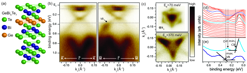
Figs. 1(b) and (c) show ARPES results of the parent compound GeBi4Te7. Band dispersions measured along the high symmetry lines and (Fig.1(b)) show the surface bands forming the typical X-shaped Dirac cones centered at within the bulk band gap. In the band map along it becomes clear that the Dirac point is only slightly above the valence band (VB) maximum which is visible on the left side (see mark in Fig. 1(b)) at the used photon energy of eV (see also next paragraph). The constant energy map at meV in Fig. 1(c) consists of a weak hexagonal contour of the surface states which enclose the conduction band (CB). The CB form a triangular structure with edges pointing in the direction. In the constant energy cut at meV in Fig. 1(c) we see the VBs forming the dominant triangular structure, pointing in the direction and a weak triangle rotated by 180∘. The VBs overlap the surface bands which are, due to the high intensity of the VB, not visible at this binding energy.
The energy distribution curves in the direction plotted in Fig.1(d) emphasize that below the Dirac point the surface states have low intensity, but they are nicely pronounced from the Dirac point heading towards the Fermi energy. The energy distribution curves at normal emission and at Å-1 in direction, where the maximum of the VB is located, show that at this photon energy the edges of the bulk bands are situated at meV for the VB and meV for the CB (Fig. 1(e)). This means the measured gap is in the range of meV with the Dirac point situated at meV. The measured band structure, especially the VB visible in the direction, is similar to the band structure of the chemically and structurally related GeBi2Te4, but the energy positions of the CB minimum, the VB maximum as well as the Dirac point differ.Okamoto et al. (2012)
SARPES measurements at a constant binding energy of 200 meV, between the Dirac point and the CB minimum, are displayed in Figs. 2(a) and (b). Only a low contribution of the bulk states to the spectral weight is expected at this energy. Accordingly, the measured spin polarization can be attributed to the surface states. The spin polarization is displayed based on a right–handed coordinate system with respect to the sample normal. The first two graphs in Fig.2(a) show the spin polarization map of the photoelectrons in the in–plane directions x and y. In the third one the out–of–plane polarization map along the z-direction is displayed. The spin polarization along a circle with a radius of Å-1 in clockwise direction are displayed in Fig.2(b). This circle corresponds roughly to the hexagonal shape of the surface bands at this binding energy.
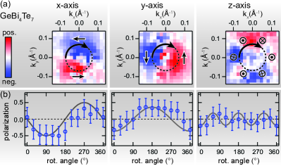
The in–plane polarization shows a helical spin orientation. This results in a splitting of the circle in the x- and y-polarization maps into semicircles with positive and negative polarization and a sinusoidal behavior with a periodicity of 360∘ in the x- and y-polarization along the circle in Fig.2(b). Along the high symmetry directions the in–plane components of the spin are completely polarized in the x- (along ) and y-direction (along ), respectively, indicated with the arrows in the corresponding polarization maps (see Fig.2(a)). An effect of the p-polarized light on the spin polarization of the photoelectrons resulting in radial in–plane polarizations between the high symmetry directions as theoretically suggested by Park and Louie (2012) was not observed. In the polarization map of the out–of–plane direction z, a sixfold symmetric buckling of the spin is visible (see right panel in Fig.2(a)). This up and down of the spin in z-direction is a result of the warping of the hexagon–shaped constant energy surface of the surface states.Fu (2009); Souma et al. (2011); Eremeev et al. (2012); Dil (2009)
Next we focus on the effects of Sb doping on the band structure of GeBi4-xSbxTe7. The following ARPES data provide evidence that under this doping it is possible to alter the band structure and tune the Fermi level towards the Dirac point. Fig.3(a) shows the ARPES measurements of five different compounds starting with the undoped sample GeBi4Te7 up to GeBi3SbTe7 (). Comparing the first two data sets, the undoped sample and the lightly doped sample (), the Dirac point as well as the position of the bulk VB shifted slightly towards the Fermi level. This rigid band shift continues at a doping of and at the CB is almost completely shifted above the Fermi level. Finally at the largest doping, in GeBi3SbTe7, the Dirac point is no longer occupied and only the lower part of the Dirac cone and the maxima of the VB cross the Fermi level. At a doping between and the Dirac point crosses the Fermi level.
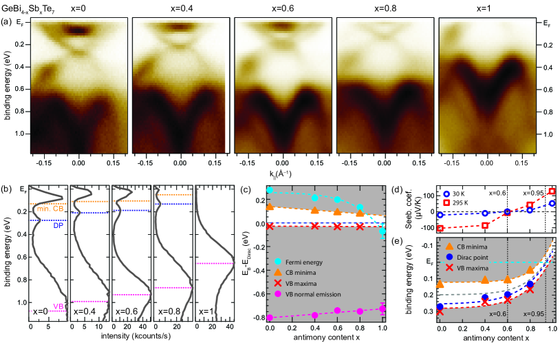
For an analysis of the band shift under Sb doping, the energetic position of Dirac point (x=0, 0.4, 0.6 and 0.8) and the broad VB feature at normal emission (all x) are fitted with Gaussian functions in the energy distribution curves in Fig. 3(b). The position of the CB minima at normal emission an the VB maxima at Å-1 were located the same way as shown in Fig.1(e) for x=0, 0.4, 0.6 and 0.8. The relative energetic positions of these points in the different band structures are plotted with respect to the Sb content in Fig.3(c), using the Dirac point as the reference. In Fig.3(c) we see, that the position of the broad VB feature at normal emission with respect to the Dirac point is a linear function of the Sb content. With an extrapolation of this linear function to the position of the VB at normal emission and accordingly the position of the Dirac point located at meV above the Fermi level can be distinguished for this compound. Comparing this position with the energetic position of the Dirac point at meV for GeBi4Te7, a band structure shift of meV over the whole doping range is observed. The energetic position of the VB maxima and the CB minima relative to the Dirac point change linearly with the Sb content as well (see Fig.3(c)). By the help of fitted linear functions the energetic positions of the VB maxima and the CB minima for GeBi3SbTe7 can be extrapolated (see Fig.3(c)). The binding energy of the Dirac point as a function of the Sb content is fitted with a sigmoid function providing a Fermi level crossing at a doping level of (see Fig.3(e)), accompanied by a n- to p-type transition of the surface transport regime.
This n- to p-type crossover is also observed in the bulk transport properties. In Fig.3(d) the composition dependence of the of GeBi4-xSbxTe7 solid solution is shown. We observe a sign change and consequently a change of the transport regime at a doping of at 30 K where the ARPES measurements were done, as well as at room temperature (see Fig.3(d)). This discrepancy between the n- to p-type transition measured at the surface and in the bulk can be explained by band bending at the sample surface, commonly known in semiconductor physics as an effect of the surface states or defect induced as observed for Bi2Se3.Zhang and Yates (2012); Bianchi et al. (2010); King et al. (2011). At a doping of , where the bulk n- to p-type transition takes place we expect the band gap center of the bulk at the Fermi level. By the help of the position of the band gap center measured in the surface region for a doping of (see Fig.3(e), dashed grey line) the downwards bending of the bands at the surface can be estimated to be 170 meV (difference between the band gap center in the surface region and in the bulk).
The measured band gap marked in Figs. 3(c) and (e) by the white region decreases linearly with Sb doping. The band gap of the undoped sample of meV is narrowing to meV for GeBi3SbTe7 if the positions of the CB minima and VB maxima are extrapolated. This narrowing of the band gap is explained by the lower atomic number of Sb compared to Bi leading to a weaker spin–orbit coupling which is responsible for the energy splitting of the bands enclosing the gap. Based on this narrowing we expect to observe the Fermi level inside the band gap in ARPES measurements for a doping between and . The observed band gap of the undoped sample is of the order of the band bending at the surface and for doped samples between and the band gap is even smaller than the band bending, assuming a constant band bending for all doping levels. Accordingly there can be no doping where a insulating bulk occurs simultaneously with a insulating surface region.
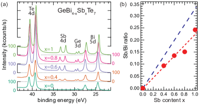
To gain further understanding of the mechanism responsible for the band shift under Sb doping the compositions of the samples were investigated by X–ray photoelectron spectroscopy (XPS). XPS data in the energy region of the Te 4d, Sb 4d, Ge 3d and Bi 5d core levels measured with a photon energy of eV are shown in Fig.4(a). In first order approximation we assume that the Sb and Bi atoms are distributed in the same atomic layers. Under these conditions the ratio of Sb to Bi is given by the peak intensities of the Sb 4d and Bi 5d core levels weighted by the respective cross sections (see Fig.4(b)). The measured ratios show a linear behavior, although their value is lower than expected from the stoichiometric composition. In XPS measurements the inelastic scattering length of the emitted electrons depends on the position of the emitting atom in the crystal. Because the exact positions of the Sb and Bi atoms in the crystal with respect to the surface and to each other is unknown, the modulation of the XPS intensities due to inelastic scattering is not known precisely which may explain the difference between the measured and the stoichiometric ratio.
The dopant Sb has the same valency as Bi, and thus it acts neither as an acceptor nor as a donor compared to Bi in GeBi4-xSbxTe7. Therefore the change in band filling as a function of increasing Sb content is not caused by carrier doping but rather by the type of defects caused by the Bi/Sb replacement. Calculations of the formation energies of the prototype case of (Bi1-xSbx)2Te3 by Niu et al. (2012) show that in the undoped Bi2Te3 sample Te vacancies and Te antisite defects (Bi replaced by Te) are dominant and are supporting the -type conductance of the compound. With increasing Sb content these defects are energetically less favorable but the building of Sb antisite defects is preferred. With less Te and more Sb antisite defects the system becomes -type. Due to the similarities of this system with GeBi4-xSbxTe7 we expect the same type of defects to be responsible for the observed - to -type transition.Niu et al. (2012); Huang et al. (2012); Zhang et al. (2011) The additional role of Ge related antisite defects could be the aim of further theoretical investigations.
The calculation of Niu et al. (2012) demonstrates also that a small change in the sample growth procedure, providing more energy during the sample formation, can open the possibility that other defects with higher formation energy may form. This as well as the sensitivity of the system to small stoichiometric changes Kuznetsov et al. (1998) is why a highly controlled sample preparation procedure with identical parameters for all the different doping levels is mandatory to reproducibly observe this change in electronic structure. We also studied samples of poorer quality who show overall features similar to what we report here, but the smooth transition of the position of the Dirac point through the Fermi energy as a function of Sb content is obscured by sample inhomogeneity.
IV Conclusion
We present (S)ARPES data of the multi–layered material GeBi4Te7 and a study of the change of the band structure under doping with Sb to GeBi4-xSbxTe7. Our data allocates spin–polarized surface states forming a freestanding Dirac point in the band gap of GeBi4Te7. Upon Sb doping we find a rigid shift of the band structure and the Dirac point crossing the Fermi level between a doping of and giving the possibility to change the surface transport regime from n- to p-type by doping. Responsible for the observed band shift is the introduction of different types of defects in the crystal structure under Sb doping. The n- to p-type transition observed in surface sensitive ARPES is clearly distinct from the transition in the bulk, visible in Seebeck coefficient measurements at . Combining these two measurements we are able to distinguish a band bending of 170 meV at the sample surface. The concluded non–coexistence of a insulating phase in the near surface region and in the bulk demonstrates the importance of the combination of bulk and surface sensitive measurements to get materials with a Fermi level in the band gap to access the topological surface states directly in transport measurements.
V Acknowledgment
We thank C. Hess, F. Dubi and M. Kropf for the technical support. This work was supported by the Swiss National Science Foundation.
References
- Kane and Mele (2005) C. L. Kane and E. J. Mele, Phys. Rev. Lett. 95, 146802 (2005).
- Hasan and Kane (2010) M. Z. Hasan and C. L. Kane, Reviews of Modern Physics 82 (2010).
- Qi and Zhang (2011) X.-L. Qi and S.-C. Zhang, Rev. Mod. Phys. 83, 1057 (2011).
- Zhang et al. (2011) J. Zhang, C.-Z. Chang, Z. Zhang, J. Wen, X. Feng, K. Li, M. Liu, K. He, L. Wang, X. Chen, Q.-K. Xue, X. Ma, and Y. Wang, Nat. Comm. 2 (2011), 10.1038/ncomms1588.
- Souma et al. (2012) S. Souma, K. Eto, M. Nomura, K. Nakayama, T. Sato, T. Takahashi, K. Segawa, and Y. Ando, Physical Review Letters 108, 116801 (2012).
- Arakane et al. (2012) T. Arakane, T. Sato, S. Souma, K. Kosaka, K. Nakayama, M. Komatsu, T. Takahashi, Z. Ren, K. Segawa, and Y. Ando, Nat. Commun. 3 (2012), 10.1038/ncomms1639.
- Hsieh et al. (2008) D. Hsieh, D. Qian, L. Wray, Y. Xia, Y. S. Hor, R. J. Cava, and M. Z. Hasan, Nature 452, 970 (2008).
- Hsieh et al. (2009a) D. Hsieh, Y. Xia, L. Wray, D. Qian, A. Pal, J. H. Dil, J. Osterwalder, F. Meier, G. Bihlmayer, C. L. Kane, Y. S. Hor, R. J. Cava, and M. Z. Hasan, Science 323, 919 (2009a), http://www.sciencemag.org/cgi/reprint/323/5916/919.pdf .
- Xia et al. (2009) Y. Xia, D. Qian, D. Hsieh, L. Wray, A. Pal, H. Lin, A. Bansil, D. Grauer, Y. S. Hor, R. J. Cava, and M. Z. Hasan, Nature Physics 5, 398 (2009).
- Chen et al. (2009) Y. L. Chen, J. G. Analytis, J.-H. Chu, Z. K. Liu, S.-K. Mo, X. L. Qi, H. J. Zhang, D. H. Lu, X. Dai, Z. Fang, S. C. Zhang, I. R. Fisher, Z. Hussain, and Z.-X. Shen, Science 325, 178 (2009).
- Nishide et al. (2010) A. Nishide, A. A. Taskin, Y. Takeichi, T. Okuda, A. Kakizaki, T. Hirahara, K. Nakatsuji, F. Komori, Y. Ando, and I. Matsuda, Phys. Rev. B 81, 041309 (2010).
- Chen et al. (2010) Y. L. Chen, Z. K. Liu, J. G. Analytis, J.-H. Chu, H. J. Zhang, B. H. Yan, S.-K. Mo, R. G. Moore, D. H. Lu, I. R. Fisher, S. C. Zhang, Z. Hussain, and Z.-X. Shen, Phys. Rev. Lett. 105, 266401 (2010).
- Kuznetsova et al. (2000) L. Kuznetsova, V. Kuznetsov, and D. Rowe, Journal of Physics and Chemistry of Solids 61, 1269 (2000).
- Zhang et al. (2009) H. Zhang, C.-X. Liu, X.-L. Qi, X. Dai, Z. Fang, and S.-C. Zhang, Nature Physics 5, 438 (2009).
- Xu et al. (2011) S.-Y. Xu, L. A. Wray, Y. Xia, F. von Rohr, Y. S. Hor, J. H. Dil, F. Meier, B. Slomski, J. Osterwalder, M. Neupane, H. Lin, A. Bansil, A. Fedorov, R. J. Cava, and M. Z. Hasan, ArXiv e-prints (2011), arXiv:1101.3985 .
- von Rohr et al. (2013) F. von Rohr, A. Schilling, and R. J. Cava, Journal of Physics: Condensed Matter 25, 075804 (2013).
- Hsieh et al. (2009b) D. Hsieh, Y. Xia, D. Qian, L. Wray, J. Dil, F. Meier, J. Osterwalder, L. Patthey, J. Checkelsky, N. Ong, A. Fedorov, H. Lin, A. Bansil, D. Grauer, Y. Hor, R. Cava, and M. Hasan, Nature 460, 1101 (2009b).
- Hoesch et al. (2002) M. Hoesch, T. Greber, V. N. Petrov, M. Muntwiler, M. Hengsberger, W. Auwaerter, and J. Osterwalder, Journal of Electron Spectroscopy and Related Phenomena 124, 263 (2002).
- Eremeev et al. (2012) S. V. Eremeev, G. Landolt, T. V. Menshchikova, B. Slomski, Y. M. Koroteev, Z. S. Aliev, M. B. Babanly, J. Henk, A. Ernst, L. Patthey, A. Eich, A. A. Khajetoorians, J. Hagemeister, O. Pietzsch, J. Wiebe, R. Wiesendanger, P. M. Echenique, S. S. Tsirkin, I. R. Amiraslanov, J. H. Dil, and E. V. Chulkov, Nat Commun 3, 103 (2012).
- Shelimova et al. (2004) L. Shelimova, O. Karpinskii, P. Konstantinov, E. Avilov, M. Kretova, and V. Zemskov, Inorganic Materials 40, 451 (2004).
- Kuznetsov et al. (1998) V. L. Kuznetsov, L. A. Kuznetsova, and D. M. Rowe, Journal of Applied Physics 85, 3207 (1998).
- Okamoto et al. (2012) K. Okamoto, K. Kuroda, H. Miyahara, K. Miyamoto, T. Okuda, Z. S. Aliev, M. B. Babanly, I. R. Amiraslanov, K. Shimada, H. Namatame, M. Taniguchi, D. A. Samorokov, T. V. Menshchikova, E. V. Chulkov, and A. Kimura, Phys. Rev. B 86, 195304 (2012).
- Park and Louie (2012) C.-H. Park and S. G. Louie, Phys. Rev. Lett. 109, 097601 (2012).
- Fu (2009) L. Fu, Phys. Rev. Lett. 103, 266801 (2009).
- Souma et al. (2011) S. Souma, K. Kosaka, T. Sato, M. Komatsu, A. Takayama, T. Takahashi, M. Kriener, K. Segawa, and Y. Ando, Phys. Rev. Lett. 106, 216803 (2011).
- Dil (2009) J. H. Dil, Journal of Physics: Condensed Matter 21, 403001 (22pp) (2009).
- Zhang and Yates (2012) Z. Zhang and J. T. Yates, Chemical Reviews 112, 5520 (2012).
- Bianchi et al. (2010) M. Bianchi, D. Guan, S. Bao, J. Mi, B. B. Iversen, P. D. C. King, and P. Hofmann, Nat Commun 1 (2010).
- King et al. (2011) P. D. C. King, R. C. Hatch, M. Bianchi, R. Ovsyannikov, C. Lupulescu, G. Landolt, B. Slomski, J. H. Dil, D. Guan, J. L. Mi, E. D. L. Rienks, J. Fink, A. Lindblad, S. Svensson, S. Bao, G. Balakrishnan, B. B. Iversen, J. Osterwalder, W. Eberhardt, F. Baumberger, and P. Hofmann, Physical Review Letters 107, 096802 (2011).
- Niu et al. (2012) C. Niu, Y. Dai, Y. Zhu, Y. Ma, L. Yu, S. Han, and B. Huang, Sci. Rep. 2 (2012), 10.1038/srep00976.
- Huang et al. (2012) F.-T. Huang, M.-W. Chu, H. H. Kung, W. L. Lee, R. Sankar, S.-C. Liou, K. K. Wu, Y. K. Kuo, and F. C. Chou, Phys. Rev. B 86, 081104 (2012).