Thermodynamic equilibrium conditions of graphene films on SiC
Abstract
First-principles surface phase diagrams reveal that epitaxial monolayer graphene films on the Si side of 3C-SiC(111) can exist as thermodynamically stable phases in a narrow range of experimentally controllable conditions, defining a path to the highest-quality graphene films. Our calculations are based on a van der Waals corrected density functional. The full, experimentally observed ()-R30∘ supercells for zero- to trilayer graphene are essential to describe the correct interface geometries and the relative stability of surface phases and possible defects.
The growth of wafer-size graphene films on a semiconducting substrate is a first step towards graphene based electronics. The semiconductor SiC as a substrate may hold the key to device applications. Here, well-ordered graphene films can be grown directly on a semiconducting substrate by a simple process (Si sublimation from the surface, e.g., Refs. Van Bommel et al. (1975); Forbeaux et al. (1998); Emtsev et al. (2009); Riedl et al. (2010); de Heer et al. (2011); Srivastava et al. (2012); Yazdi et al. (2013)) and the standard tools of semiconductor technology can be used for further manipulation. Indeed, graphene-based devices and even integrated circuits Lin et al. (2011); Hertel et al. (2012) were already created on the Si side of SiC substrates. However, controlling the precise thickness of graphene films is important to minimize the coexistence of monolayer graphene (MLG) and bilayer graphene (BLG).Berger et al. (2004); Emtsev et al. (2009); First et al. (2010); de Heer et al. (2011) MLG areas exhibit no band gap, while BLG areas do.Riedl et al. (2010) A recent, joint experimental-theoretical study finds particularly high local resistances across monolayer-bilayer graphene junctions on the same surface,Ji et al. (2011) a possible contributing factor to low carrier mobilities in graphene on SiC(0001).Emtsev et al. (2009); Ji et al. (2011)
The growth of graphene on SiC is special in the sense that, instead of offering one or more of the components from the gas phase, graphene areas are formed by controlled sublimation of Si from the surface.Van Bommel et al. (1975); Forbeaux et al. (1998) Graphene films grown under ultrahigh vacuum conditions are typically inhomogeneous.Emtsev et al. (2009); de Heer et al. (2011) To improve their quality is therefore a major and ongoing experimental goal.Emtsev et al. (2009); de Heer et al. (2011) In the past, the appearance of different phases was often interpreted Emtsev et al. (2008); Ming and Zangwill (2011); de Heer et al. (2011) as intuitive, successive intermediates formed by an outgoing Si flux that ultimately leads to bulk-like graphite layers. If graphene films of various thicknesses were a result of a purely kinetically limited Si sublimation process (controlled by growth temperature and time), improving upon the homogeneity of the layer thickness would be difficult. It would be helpful if there were a set of thermodynamic equilibrium conditions (e.g., temperature and partial pressures of Si and C Reuter and Scheffler (2001)) at which a desired film thickness were thermodynamically stable over all others. As long as is sufficiently high to overcome the relevant kinetic barriers, large-scale ordered films of that particular thickness could then be formed simply by finding and maintaining () near these equilibrium conditions.
In fact, experimental evidence is mounting that controlled conditions do indeed aid the growth of graphene on SiC. Ref. Tromp and Hannon (2009) demonstrates that the carbon-rich “zero-layer graphene” (ZLG) or “buffer layer” precursor phase Van Bommel et al. (1975); Forbeaux et al. (1998); Riedl et al. (2007); Emtsev et al. (2008) (not yet graphene) on the Si face is a reversible thermodynamic equilibrium phase at high with a controlled disilane background pressure. Reversibility is much harder to demonstrate once a complete graphene plane is formed,Hannon (2012) but an increased growth temperature in an Ar background buffer gas does lead to much improved MLG film homogeneity.Emtsev et al. (2009) Excellent wafer-size MLG films are also reported for growth in a confined cavity that may retain a finite, well-defined Si background pressure as Si evaporates from the surface.de Heer et al. (2011) Finally, a well-defined graphene precursor phase on the C face at finite disilane background pressure was reported very recently.Srivastava et al. (2012) What is still not clear, however, is whether MLG itself is an equilibrium phase under certain conditions. If so, one could ideally facilitate the growth of MLG but not BLG on SiC(111).
We here present first-principles theoretical evidence that such equilibrium conditions indeed exist for MLG (and, possibly, even BLG) on the Si face of SiC(111). We employ density-functional theory (DFT) using the van der Waals (vdW) corrected Tkatchenko and Scheffler (2009) PBE density functionalPerdew et al. (1997) (called PBE+vdW throughout this work). Strategies to include vdW effects have become an active scientific area of their own (see, e.g., Refs. Grimme (2011); Dion et al. (2004); Lee et al. (2010); Klimes et al. (2010); Zhang et al. (2011); Tkatchenko et al. (2012) and many references therein). However, for the large, complex carbon-rich interfaces of interest here, no unambiguously quantitatively improved approach over the level of theory used here exists to our knowledge, i.e., the present incorporation of vdW terms reflects the state of the art. For the structure of the relevant bulk phases, the impact of different standard functionals is well understood and systematic. Predicted lattice parameters (see supporting information (SI) for full reference datasup ) for 3C SiC are within 1 % of PBE+vdW and experiment: 4.33 Å, 4.38 Å, 4.36 Å, respectively, for the local density approximation (LDA), PBE without vdW, and PBE+vdW. Similary small discrepancies arise for diamond C and for the in-plane lattice parameter of graphite: =2.45 Å (LDA), 2.47 Å (PBE), 2.46 Å (PBE+vdW). Zero-point corrections (ZPC) to the lattice parameters are also below 1 %.sup . For the interplanar lattice parameter of graphite, vdW effects must be included into the PBE functional (LDA: 6.65 Å, PBE+vdW: 6.66 Å, but 8.65 Å for PBE). On a technical level, our calculations are based on the FHI-aims all-electron codeBlum et al. (2009); Havu et al. (2009) with “tight” numerical settings and the massively parallel ELPA eigensolver libraryAuckenthaler et al. (2011) to guarantee accurate total energies for the very large structure sizes involved (see SI for details sup ).
In experiment, one encounters a series of phases on the Si side of 3C-SiC(111) (experimentally also observed on the Si side of 4H-SiC(0001) and 6H-SiC(0001)) when going from a Si-rich to a C-rich regime. In UHV, a (33) Si-rich layer Starke et al. (1998) can be prepared. Upon Si sublimation, a simpler ()-R30∘ bulk-terminated surface with one adsorbed Si adatom per three unit cells follows. kap (1989); Starke et al. (1999) Removing yet more Si creates a partially covalently bonded carbon “buffer layer,” the ZLG phase, with a large, commensurate unit cell: One (1313) honeycomb graphene-like supercell (338 C atoms) on a (66)-R30∘ mesh (108 Si and 108 C atoms per bilayer) of the underlying SiC substrate.Van Bommel et al. (1975) Compared to a graphene plane in graphite, the lattice match is almost strain-free (experiment: 0.2 % at =0 K Li and Bradt (1986); Baskin and Meyer (1955), PBE+vdW: 0.1 % sup ). The ZLG phase does not yet exhibit the electronic properties of actual freestanding graphene.Emtsev et al. (2008) Further heating detaches the ZLG C plane from the substrate to form MLG and a new C-rich layer underneath.Seyller et al. (2008); Hannon et al. (2011) The same process can be continued to successively form BLG Ohta et al. (2006) and multilayer graphene films. Importantly, our calculations address the graphene-like films in their experimentally observed, large commensurate ()-R30∘ supercells, using slabs containing six Si-C bilayers under each reconstructed phase (1,742 up to 2,756 atoms for ZLG up to three-layer graphene (3LG), respectively). The top three SiC bilayers and all planes above are fully relaxed (residual energy gradients: 810-3 eV/Å or below).
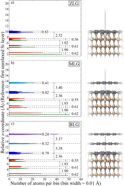
Figures 1a-c show the ZLG, MLG and BLG phases together with key geometry parameters predicted at the level of PBE+vdW. Since all planes are corrugated,Kim et al. (2008); Varchon et al. (2008); Sclauzero and Pasquarello (2012a) histograms for the atomic coordinates are included. The interface geometry stays essentially the same despite the addition of more graphene planes. In the MLG phase, we see a significant buckling of the topmost graphene layer (0.41 Å between top and bottom of the plane). This strong buckling is qualitatively consistent with existing STM images Chen et al. (2005); De Heer et al. (2010); Berger et al. (2010). In the BLG phase, the corrugation is slightly reduced, but the two top planes are still buckled by 0.24 Å and 0.32 Å, respectively. This buckling reflects some coupling to the covalently bonded interface C-rich plane, which is much more corrugated (0.8 Å in our work, similar to experimental estimatesGoler et al. (2013); de Lima et al. (2013)). The observed graphene interplanar distances near the interface are slightly expanded compared to experimental bulk graphite (3.34 Å Baskin and Meyer (1955)) and in good qualitative agreement with estimates from scanning tunneling microscopy Berger et al. (2010) and transmission electron microscopy.Norimatsu and Kusunoki (2009)
We have also compared our findings to geometries for the straight PBE functional (no vdW correction), and for the local-density approximation (LDA). In PBE, the C-C interplanar distances are unphysically expanded (4.42 Å for MLG). In contrast, the LDA geometry of the carbon planes agrees qualitatively with PBE+vdW, although LDA incorporates no long-range vdW interactions. The first qualitative geometry difference between the PBE+vdW and LDA treatments appears in the Si part of the top Si bilayer, where some Si atoms (those with dangling bonds pushing against the -bonded parts of the C interface plane Varchon et al. (2007)) are located much deeper (by 0.3 Å) in PBE and PBE+vdW than in LDA. A direct crystallographic verification would be desirable.
In a grand canonical formalism, the possible equilibrium conditions for different surface phases can be represented by the chemical potentials of C and Si, and . In experiment, and can be manipulated, e.g., through the substrate temperature and background pressure of gases that supply Si or C.Reuter and Scheffler (2001); Tromp and Hannon (2009); de Heer et al. (2011); Srivastava et al. (2012). Consider the surface energies of a two-dimensional periodic SiC slab with a C face and a Si face. In the limit of sufficiently thick slabs, we have:
| (1) |
and denote the number of Si and C atoms in the slab, respectively, and is the chosen area. All our surface energies are in eV per area of a (11) SiC unit cell. The letter denotes total energies for a given atomic geometry throughout this work. In our actual calculations, we always choose a fixed H-terminated C-face geometry, which cancels out for all surface energy differences related to the Si face.
The major experimental () dependence during growth arises through the reservoirs of Si and C, which define and .Reuter and Scheffler (2001); Tromp and Hannon (2009) Thus, a precise control of background gases as reservoirs (for instance, disilane Tromp and Hannon (2009)) is desirable, even if calibration variationsLu et al. (2010) may require exact () ranges to be adjusted separately for a given growth chamber. The actual growth process proceeds by Si out-diffusion from underneath already formed graphene planes. Yet, the external Si reservoir background pressure still matters in equilibrium: As long as the diffusion path to the outside remains open, so does the inward diffusion path, and near equilibrium with the reservoir gas can be achieved. During intermediate stages of the formation of a new graphene plane,Norimatsu and Kusunoki (2009) such diffusion paths must be available.
In principle, we could further include the much smaller () dependence of the solid phases by focusing on Gibbs free energies in the (quasi-)harmonic approximation instead of . However, quantifying this dependence precisely would here necessitate accurate phonon calculations for structure sizes of the order of 2,000 atoms, a task that is computationally prohibitive at present. ZPC are small for the bulk phases (see SI sup ). Still, the possible small contribution of finite stresses at the growth conditionsRoehrl et al. (2008) is kept in mind when interpreting our calculated results below.
In equilibrium with a stable SiC bulk, and are linked through
| (2) |
The energies are per atom, and is the formation enthalpy of SiC with respect to the elemental C and Si. The bulk phases define the chemical potential limits within which the SiC crystal is stable against decomposition into bulk Si or C: and , leading to
| (3) |
and analogous for Si. The diamond structure for Si is the appropriate bulk phase, but for C, there is a close competition between diamond and graphite.Berman and Simon (1955); Yin and Cohen (1984) We thus include both phases in our analysis.
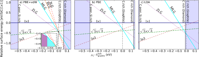
The experimentally reported energy difference between diamond and graphite at =0 K is 25 meV/atom Berman and Simon (1955). Based on the potential energy minima (no ZPC) graphite is found to be more stable than diamond in PBE+vdW by 60 meV/atom (Fig. 2a). This is qualitatively consistent with the extrapolated experimental phase hierarchy. In plain PBE graphite is overstabilized by 130 meV/atom. In LDA, both phases are similarly stable: Considering only the potential energy surface, diamond is slightly more stable (by 12 meV), but already the inclusion of ZPCYin and Cohen (1984) would neutralize this balance (graphite more stable by 3 meV/atomLazarevic et al. (2013)).
The surface energies of the known surface phases of SiC (Si face) are shown as a function of in Fig. 2a for PBE+vdW. The most stable phase for a given value of is that with the lowest surface energy. Going through Fig. 2a from left to right, we find the expected broad ranges of stability for the Si-rich (33) and ()-R30∘ phases. Just before the C-rich limit (bulk graphite) is reached, there is a crossover first to ZLG, then to MLG, and even to a very narrow slice of the BLG phase. As an additional bound, ABA-stacked trilayer graphene (3LG) is also shown, crossing BLG within 1 meV of bulk graphite.
While the respective stability ranges are narrow (inset of Fig. 2a: 4 meV, 5 meV and 1 meV for ZLG, MLG and BLG, respectively at the chemical potential axis), but it is important to recall that narrow chemical potential ranges do not necessarily correspond to narrow experimental conditions: A drastic change in the number of Si () and C () atoms can correspond to a small change of . For instance, one would first have to remove all Si from the SiC crystal to cross beyond the graphite stability line in equilibrium. However, the surface-energy differences between the different phases are also rather small (a few tens of meV per (11) SiC surface unit cell). The primary approximations that we cannot systematically improve in our calculations are the density functional used, as well as possible small temperature-dependent surface strain effects (see above). The key message of Fig. 2a is thus that MLG and its related phases all appear at least as very near equilibrium phases, a fact that is nonetheless critical for a qualitatively correct understanding of their growth and properties.
What we can do is to show how our results would be affected by different density-functional treatments. We have thus recomputed the surface phase diagram up to the MLG phase for two widely used functionals in Figs. 2b and c: the plain PBE functional, which lacks long-range vdW interactions and should thus yield untrustworthy results, and for the often used LDA functional. As expected, the absence of vdW tails in the plain PBE functional changes the phase diagram drastically. Due to the overstabilization of graphite (130 meV/atom), its stability line moves significantly further to the left, as does the crossover point between ZLG and MLG. As a result, neither ZLG nor MLG becomes stable over the competing Si-rich ()-R30∘ phase in PBE, in outright contradiction to experiment.Tromp and Hannon (2009) In the LDA-derived phase diagram, the most significant change compared to PBE+vdW is the apparent incorrect stability hierarchy of graphite vs. diamond (without ZPC). If the diamond line were discounted, our calculations show the ZLG-MLG crossover point almost exactly on the graphite line. Still, even taking LDA at face value implies the existence of - conditions very close to equilibrium for MLG, making the experimental search for such conditions promising.
Figure 2 thus shows the most important point of our paper: The existence of equilibrium or near-equilibrium chemical potential ranges for ZLG, MLG, and even BLG, corresponding to specific / conditions in experiment. For each phase, this finding proves the potential for much better growth control than what could be expected if each phase were just a necessary (but not thermodynamically stable) kinetic intermediate. While true reversibility for actual MLG may be hard to achieve Tromp and Hannon (2009); Hannon (2012) (the reverse growth process, disassembling a fully formed graphene plane would be kinetically difficult), the active forward growth process from MLG to BLG under Si out-diffusion should still be limitable by appropriate / conditions. A macroscopically homogeneous surface very close to pure-phase MLG should thus be achievable in principle.
Figure 2 shows unambiguously the importance of a consistently accurate numerical treatment of the experimentally observed phases in their large unit cells. It would obviously be much more economical to consider smaller-cell approximant phases to the true (66)-R30∘ supercells. However, the residual artificial strain and inadequate bonding in those phases are too large for meaningful surface energy comparisons.Sclauzero and Pasquarello (2012b) For instance, the popular ()-R30∘ Varchon et al. (2007); Mattausch and Pankratov (2007) approximant would intersect the graphite stability line at a surface energy =0.15 eV, far above the actually stable phases. Likewise, a slightly rotated (55) approximant to the ZLG phasePankratov et al. (2010) (a periodicity sometimes seen in experimentRiedl et al. (2007); Starke and Riedl (2009)) would intersect at (=0.35 eV), still higher by 0.06 eV than even the closest competing Si-rich phase, the ()-R30∘ Si adatom phase ( eV). The (55) phase is either a nonequilibrium phase, or its structure is not the same as that assumed in Ref. Pankratov et al. (2010).
The true problem with artificially strained approximant phases is that the resulting strain can obscure other electronically relevant properties, such as the energetics of defects. As an example, we consider a specific class of C-rich defects suggested as an equilibrium feature of the ZLG phase in Ref. Qi et al. (2010). Two different defect positions, “hollow” and “top” were suggested.Qi et al. (2010) Indeed, both would be more stable than the hypothetical ()-R30∘ ZLG approximant when included there in a arrangement as done in Ref. Qi et al. (2010): 1.75 eV per defect for the hollow position, 2.93 eV per defect for top, both at . However, the same defects are unstable when included into and compared to the correct ()-R30∘ ZLG phase: 5.28 eV per defect for hollow, 5.27 eV for top, again at (see SIsup for structure and other details).
In conclusion, we can now rationalize some specific growth-related
observations:
(1) When simply heating a sample in UHV, the background pressures of Si and C are low and
ill-defined. The observed inferior morphologies and wide
variations of experimental conditionsSutter (2009); Lu et al. (2010) are consistent with
this picture.
(2) Much more homogeneous growth can be achieved in an Ar atmosphere,Emtsev et al. (2009)
although MLG/BLG phase areas still coexist. A uniform background partial pressure of
Si, however, will not be strictly guaranteed.
(3) The observed thermodynamic ZLG stability and improved growth of MLG
by controlling a disilane reservoir Tromp and Hannon (2009) is fully consistent with our
findings.
(4) The use of a confined cavity to control the Si flux away from the sample reportedly
yields excellent wafer-size films.de Heer et al. (2011) Maintaining a controlled Si partial
pressure at constant temperature is most likely the important step.
(5) Finally, similar considerations may also aid the much more difficult
growth of MLG on the C face.de Heer et al. (2011); Hass et al. (2007) While our work is
restricted to the Si face, a well-defined interface layer on the C face at finite disilane
background pressure was proposed very recently.Srivastava et al. (2012) This finding is an
excellent additional indication that near-equilibrium surface conditions are indeed the
key to the best possible epitaxial growth of graphene on SiC.
References
- Van Bommel et al. (1975) A. Van Bommel, J. Crombeen, and A. Van Tooren, Surf. Sci. 48, 463 (1975).
- Forbeaux et al. (1998) I. Forbeaux, J.-M. Themlin, and J.-M. Debever, Phys. Rev. B 58, 16396 (1998).
- Emtsev et al. (2009) K. V. Emtsev, A. Bostwick, K. Horn, J. Jobst, G. L. Kellogg, L. Ley, J. L. McChesney, T. Ohta, S. A. Reshanov, J. Röhrl, et al., Nature Materials 8, 203 (2009).
- Riedl et al. (2010) C. Riedl, C. Coletti, and U. Starke, J. Phys. D: Appl. Phys. 43, 374009 (2010).
- de Heer et al. (2011) W. A. de Heer, C. Berger, M. Ruan, M. Sprinkle, X. Li, Y. Hu, B. Zhang, J. Hankinson, and E. Conrad, Proc. Nat. Acad. Sci. 108, 16900 (2011).
- Srivastava et al. (2012) N. Srivastava, G. He, Luxmi, and R. M. Feenstra, Phys. Rev. B 85, 041404 (2012).
- Yazdi et al. (2013) G. R. Yazdi, R. Vasiliauskas, T. Iakimov, A. Zakharov, M. Syväjärvi, and R. Yakimova, Carbon 57, 477 (2013).
- Lin et al. (2011) Y. Lin, A. Valdes-Garcia, S. Han, D. Farmer, I. Meric, Y. Sun, Y. Wu, C. Dimitrakopoulos, A. Grill, P. Avouris, et al., Science 332, 1294 (2011).
- Hertel et al. (2012) S. Hertel, D. Waldmann, J. Jobst, A. Albert, M. Albrecht, S. Reshanov, A. Schöner, M. Krieger, and H. Weber, Nature Comm. 3, 957 (2012).
- Berger et al. (2004) C. Berger, Z. Song, T. Li, X. Li, A. Ogbazghi, R. Feng, Z. Dai, A. Marchenkov, E. Conrad, N. Phillip, et al., J. Phys. Chem. B 108, 19912 (2004).
- First et al. (2010) P. First, W. De Heer, T. Seyller, C. Berger, J. Stroscio, and J. Moon, MRS Bulletin 35, 296 (2010).
- Ji et al. (2011) S.-H. Ji, J. B. Hannon, R. M. Tromp, V. Perebeinos, J. Tersoff, and F. M. Ross, Nature Materials (2011).
- Emtsev et al. (2008) K. V. Emtsev, F. Speck, T. Seyller, L. Ley, and J. D. Riley, Phys. Rev. B 77, 155303 (2008).
- Ming and Zangwill (2011) F. Ming and A. Zangwill, Phys. Rev. B 84, 115459 (2011).
- Reuter and Scheffler (2001) K. Reuter and M. Scheffler, Phys. Rev. B 65, 035406 (2001).
- Tromp and Hannon (2009) R. M. Tromp and J. B. Hannon, Phys. Rev. Lett. 102, 106104 (2009).
- Riedl et al. (2007) C. Riedl, U. Starke, J. Bernhardt, M. Franke, and K. Heinz, Phys. Rev. B 76, 245406 (2007).
- Hannon (2012) J. B. Hannon (2012), private communication.
- Tkatchenko and Scheffler (2009) A. Tkatchenko and M. Scheffler, Phys. Rev. Lett. 102, 073005 (2009).
- Perdew et al. (1997) J. P. Perdew, K. Burke, and M. Ernzerhof, Phys. Rev. Lett. 78, 1396 (1997).
- Grimme (2011) S. Grimme, Comput. Mol. Sci. 1, 211 (2011).
- Dion et al. (2004) M. Dion, H. Rydberg, E. Schröder, D. C. Langreth, and B. I. Lundqvist, Phys. Rev. Lett. 92, 246401 (2004).
- Lee et al. (2010) K. Lee, É. D. Murray, L. Kong, B. I. Lundqvist, and D. C. Langreth, Phys. Rev. B 82, 081101 (2010).
- Klimes et al. (2010) J. Klimes, D. R. Bowler, and A. Michaelides, J. Phys.: Condens. Matter 22, 022201 (2010).
- Zhang et al. (2011) G. X. Zhang, A. Tkatchenko, J. Paier, H. Appel, and M. Scheffler, Phys. Rev. Lett. 107, 245501 (2011).
- Tkatchenko et al. (2012) A. Tkatchenko, R. A. DiStasio, R. Car, and M. Scheffler, Phys. Rev. Lett. 108, 236402 (2012).
- (27) See supplementary material. The supplementary material includes reference data for the numerical convergence of our calculations, calculated lattice parameters and other cohesive properties of the bulk reference phases 3C-SiC, diamond Si, diamond and graphite C, without and with zero-point corrections for the functionals used here, and structural details of the exemplary defects as introduced in Ref. Qi et al. (2010).
- Blum et al. (2009) V. Blum, R. Gehrke, F. Hanke, P. Havu, V. Havu, X. Ren, K. Reuter, and M. Scheffler, Comp. Phys. Commun. 180, 2175 (2009).
- Havu et al. (2009) V. Havu, V. Blum, P. Havu, and M. Scheffler, J. Comp. Phys. 228, 8367 (2009).
- Auckenthaler et al. (2011) T. Auckenthaler, V. Blum, H. Bungartz, T. Huckle, R. Johanni, L. Krämer, B. Lang, H. Lederer, and P. Willems, Parallel Computing 37, 783 (2011).
- Starke et al. (1998) U. Starke, J. Schardt, J. Bernhardt, M. Franke, K. Reuter, H. Wedler, K. Heinz, J. Furthmüller, P. Käckell, and F. Bechstedt, Phys. Rev. Lett. 80, 758 (1998).
- kap (1989) Surf. Sci. 215, 111 (1989).
- Starke et al. (1999) U. Starke, J. Schardt, J. Bernhardt, M. Franke, and K. Heinz, Phys. Rev. Lett. 82, 2107 (1999).
- Li and Bradt (1986) Z. Li and R. C. Bradt, J. Mat. Sci. 21, 4366 (1986).
- Baskin and Meyer (1955) Y. Baskin and L. Meyer, Phys. Rev. 100, 544 (1955).
- Seyller et al. (2008) T. Seyller, A. Bostwick, K. Emtsev, K. Horn, L. Ley, J. McChesney, T. Ohta, J. Riley, E. Rotenberg, and F. Speck, phys. stat. sol. (b) 245, 1436 (2008).
- Hannon et al. (2011) J. B. Hannon, M. Copel, and R. M. Tromp, Phys. Rev. Lett. 107, 166101 (2011).
- Ohta et al. (2006) T. Ohta, A. Bostwick, T. Seyller, K. Horn, and E. Rotenberg, Science 313, 951 (2006).
- Kim et al. (2008) S. Kim, J. Ihm, H. J. Choi, and Y. W. Son, Phys. Rev. Lett. 100, 176802 (2008).
- Varchon et al. (2008) F. Varchon, P. Mallet, J.-Y. Veuillen, and L. Magaud, Phys. Rev. B 77, 235412 (2008).
- Sclauzero and Pasquarello (2012a) G. Sclauzero and A. Pasquarello, Phys. Rev. B 85, 161405(R) (2012a).
- Chen et al. (2005) W. Chen, H. Xu, L. Liu, X. Gao, D. Qi, G. Peng, S. C. Tan, Y. Feng, K. P. Loh, and A. T. S. Wee, Surf. Sci. 596, 176 (2005).
- De Heer et al. (2010) W. De Heer, T. Seyller, C. Berger, J. Stroscio, and J. Moon, MRS Bulletin 35, 296 (2010).
- Berger et al. (2010) C. Berger, J. Veuillen, L. Magaud, P. Mallet, V. Olevano, M. Orlita, P. Plochocka, C. Faugeras, G. Martinez, M. Potemski, et al., Int. J. Nanotechnol. 7, 383 (2010).
- Goler et al. (2013) S. Goler, C. Coletti, V. Piazza, P. Pingue, F. Colangelo, V. Pellegrini, K. V. Emtsev, S. Forti, U. Starke, F. Beltram, et al., Carbon 51, 249 (2013).
- de Lima et al. (2013) L. H. de Lima, A. de Siervo, R. Landers, G. A. Viana, A. M. B. Goncalves, R. G. Lacerda, and P. Häberle, Phys. Rev. B 87, 081403(R) (2013).
- Norimatsu and Kusunoki (2009) W. Norimatsu and M. Kusunoki, Chem. Phys. Lett. 468, 52 (2009).
- Varchon et al. (2007) F. Varchon, R. Feng, J. Hass, X. Li, B. Nguyen, C. Naud, P. Mallet, J. Veuillen, C. Berger, E. Conrad, et al., Phys. Rev. Lett. 99, 126805 (2007).
- Lu et al. (2010) W. Lu, J. J. Boeckl, and W. C. Mitchell, J. Phys. D: Appl. Phys. 43, 374004 (2010).
- Roehrl et al. (2008) J. Roehrl, M. Hundhausen, K. Emtsev, T. Seyller, R. Graupner, and L. Ley, Appl. Phys. Lett. 92, 201918 (2008).
- Berman and Simon (1955) R. Berman and F. Simon, Z. f. Elektrochem.: Ber. Bunsenges. Phys. Chem. 59, 333 (1955).
- Yin and Cohen (1984) M. T. Yin and M. L. Cohen, Phys. Rev. B 29, 6996 (1984).
- Lazarevic et al. (2013) F. Lazarevic, L. Nemec, V. Blum, and M. Scheffler, to be published (2013).
- Sclauzero and Pasquarello (2012b) G. Sclauzero and A. Pasquarello, Diamond Rel. Materials 23, 178 (2012b).
- Mattausch and Pankratov (2007) A. Mattausch and O. Pankratov, Phys. Rev. Lett. 99, 076802 (2007).
- Pankratov et al. (2010) O. Pankratov, S. Hensel, and M. Bockstedte, Phys. Rev. B 82, 121416 (2010).
- Starke and Riedl (2009) U. Starke and C. Riedl, J. Phys.: Condens. Matter 21, 134016 (2009).
- Qi et al. (2010) Y. Qi, S. H. Rhim, G. F. Sun, M. Weinert, and L. Li, Phys. Rev. Lett. 105, 085502 (2010).
- Sutter (2009) P. Sutter, Nature Materials 8, 171 (2009).
- Hass et al. (2007) J. Hass, R. Feng, J. E. Millán-Otoya, X. Li, M. Sprinkle, P. N. First, W. A. de Heer, E. H. Conrad, and C. Berger, Phys. Rev. B 75, 214109 (2007).