To see or not to see: Imaging surfactant coated nano–particles using HIM and SEM
Abstract
Nano–particles are of great interest in fundamental and applied research. However, their accurate visualization is often difficult and the interpretation of the obtained images can be complicated. We present a comparative scanning electron microscopy and helium ion microscopy study of cetyltrimethylammonium–bromide (CTAB) coated gold nano–rods. Using both methods we show how the gold core as well as the surrounding thin CTAB shell can selectively be visualized. This allows for a quantitative determination of the dimensions of the gold core or the CTAB shell. The obtained CTAB shell thickness of 1.0 nm–1.5 nm is in excellent agreement with earlier results using more demanding and reciprocal space techniques.
keywords:
Helium Ion Microscopy , Scanning Electron Microscopy , Nano–particles1 Introduction
Today, nano–particles can be synthesized with a variety of shapes [1, 2, 3, 4, 5] and arrangements [6, 7], allowing for different applications. To unveil the full potential of these nano–particle based applications [8, 9] in general, it is imperative to understand and characterize the wide range of intriguing properties of these nanoscale entities. Important structural and compositional information can be obtained from high resolution imaging of these particles in their native form. It is crucial to realize that not only the shape but also the nearly always present surfactant layer influences the properties of the nano–particles [10].
Scanning Electron Microscopy (SEM) is routinely used to obtain information on the shape, size and arrangement of nano–particles. This method is very successful in this research field as it is minimal invasive and can achieve the required resolution of a few nano–meters down into the sub–nanometer range [11]. With the advent of new detectors that allow energy filtering and separation of the different contributions to the signal as well as the possibility to use ultra–low acceleration voltages, the surface sensitivity of the method has also increased substantially. Alternatively, a new charged particle scanning beam microscopy method has entered the market a few years ago. Helium Ion Microscopy (HIM) [12] has an ultimate resolution as small as 0.29 nm [13, 11] and a very high surface sensitivity [14]. It uses helium ions to generate a multitude of signals including secondary electrons (SE), backscattered helium (BSHe) and photons.
Despite their obvious advantages, both methods—SEM [15] as well as HIM [16]—are plagued by carbon deposition in the scanned area. This carbon deposition reduces image quality and in particular hinders the detection of ultra–thin carbon layers intentionally present on the sample. HIM is particularly sensitive to this effect for two reason. Firstly, helium ions with a typical energy of 30 kV are very efficient in cracking hydrocarbons present on the sample surface. These hydrocarbons are either present on the sample and/or replenished from the vacuum during imaging. Secondly, due to the high surface sensitivity of HIM already very thin layers of carbon will be visible in the image. In particular the last point also applies for very low–voltage SEM. However, applying appropriate cleaning procedures to the chamber as well as the sample prior to imaging this problem can be eliminated. Provided that deposition of carbon from the chamber vacuum can be excluded a very high sensitivity for intentionally deposited ultra–thin carbon layers is possible in HIM [14].
As a result of the surfactant assisted fabrication routes nano–particles are usually covered by such a thin carbon based layer. In the case discussed here, gold nano–rods are covered with an interdigiting double layer of cetyltrimethylammonium (CTA) which is formed during synthesis using CTA–bromide (CTAB). Comparison of Small Angle X–ray Scattering (SAXS) and Transmission Electron Microscopy (TEM) measurements revealed that the thickness of this shell is between 1.0 nm and 1.5 nm [17]—and thus less than the length of a single stretched CTA molecular ion of 2.2 nm [18].
In this paper we will present high–resolution images of CTAB/Au core–shell nano–particles obtained with SEM and HIM. In this context the underlying reasons for the visibility of either the gold–core or CTAB–shell in the different imaging modes will be discussed. By comparing core and shell we show that the thickness of the CTA layer can be measured with sufficient accuracy reducing the necessity for more elaborate measurement strategies such as SAXS and TEM.
2 Materials and methods
2.1 Nano–rod preparation
CTAB–stablized gold nano–rods of aspect ratios 4 and 5 were synthesized using a seed–mediated synthesis [5]. To remove excess CTAB from the suspensions, they were centrifuged at 15000 rpm for 10 minutes. The supernatant was carefully removed, leaving the sedimented nano–rods in the bottom of the centrifugetube. Finally, the nano–particles were resuspended in the same amount of Milli–Q water. This procedure was performed twice. In addition, the suspensions were centrifuged at 5600 rpm for 5 minutes to eliminate most spheres from the suspension. Ultraviolet–visible (UV–VIS) spectroscopy was used to identify typical resonances in the as–prepared nano–particles consisting of rods and some remaining spheres. The longitudinal peaks were situated at 800 nm and 860 nm for nano–rods of aspect ratio 4 and 5, respectively. The corresponding rod lengths amount to 45 nm5 nm for aspect ratio 4 and 55 nm5 nm for aspect ratio 5. The width of all rods is between 10 nm and 12 nm. Samples were prepared for HIM and SEM analysis, by drop–casting 30 µl of each suspension onto a clean SiO2 substrate. Within 2 h the liquid has completely evaporated, leaving a coffee–stain ring of gold nano–particles. No further sample conditioning was necessary for the subsequent SEM and HIM imaging.
2.2 Charged particle beam microscopy
HIM measurements were performed using an ultra–high vacuum (UHV) Orion Plus helium ion microscope from Zeiss [16]. The microscope is equipped with an Everhardt–Thornley (ET) detector for Secondary Electron (SE) detection. A micro–channel plate situated below the last lens just above the sample allows the qualitative analysis of Backscattered Helium (BSHe). This detector yields images in which dark corresponds to light elements—having a low backscatter probability—and bright areas—with a high backscatter yield—correspond to heavy elements in the specimen.
High Resolution Scanning Electron Microscopy (HRSEM) measurements were performed using a Merlin Field Emission SEM (FE–SEM) from Zeiss. The microscope is equipped with a on–axis in–lens secondary electron detector as well as a high efficiency off–axis secondary electron detector. The in–lens detector—which has been used in this study—is a high efficiency detector for SE1 and SE2 and owes its superb imaging results to the geometric position in the beam path and the combination with the electrostatic/electromagnetic lens. This detector is in particular powerful at low voltages provided a small working distance can be reached.
2.3 Simulation methods
In order to asses the yield and origin of secondary electrons as well as backscattered electrons in SEM, Monte Carlo simulations using CASINO [19] have been utilized. The sample was modeled using a 2 nm thick carbon layer on a 10 nm thick gold slab on top of a silicon substrate. The density of the carbon layer has been manually set to 0.5 g/cm3. Secondary electron and backscattered electron yields were calculated as well as the distribution.
SRIM [20] calculations have been used to obtain insight into the contrast ratios for backscattered helium images. Backscatter yields for nano–rods and CTA covered silicon were calculated using the Kinchin–Pease approximation. The same sample setup as above has been used with the exception that the carbon layer has been replaced with a layer of CTA stoichiometry and a density of 0.5 g/cm3.
3 Results
In fig. 1(A) a HIM image of gold nano–rods is presented. The image has been obtained from an area covered by several layers of nano–rods. An acceleration voltage of 34.9 keV and an ion dose of cm-2 were used. Although the alignment of the rods is visible, the blanket covering them makes the recognition of individual rods difficult. This blanket is formed from residues—mostly CTAB—of the nano–rod synthesis. However, a SEM image of the same area is presented in fig. 1(B). An acceleration voltage of 0.7 keV and a probe current of 50 pA has been used to record the image. Here, the rods are clearly visible and the CTAB blanket is only visible where it is very thick (e.g. in the upper right corner of the hole). The effect of the blanket is best seen by comparing the area marked with an arrow. From the two crevices visible in the SEM image one is not visible at all while the other is barely visible in the HIM image.
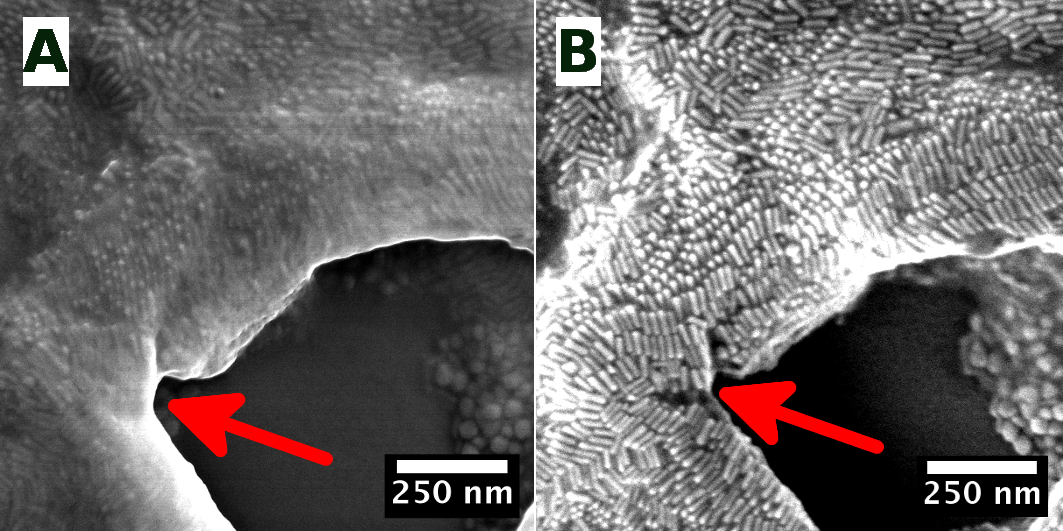
Figure 2 shows high resolution HIM images and cross sections obtained from an area with a low density of gold nano–rods. The image has been recorded using an acceleration voltage of 20 kV and an ion dose of cm-2. This corresponds to 375 ions per pixel. A larger working distance had to be chosen to accommodate the BSHe detector.
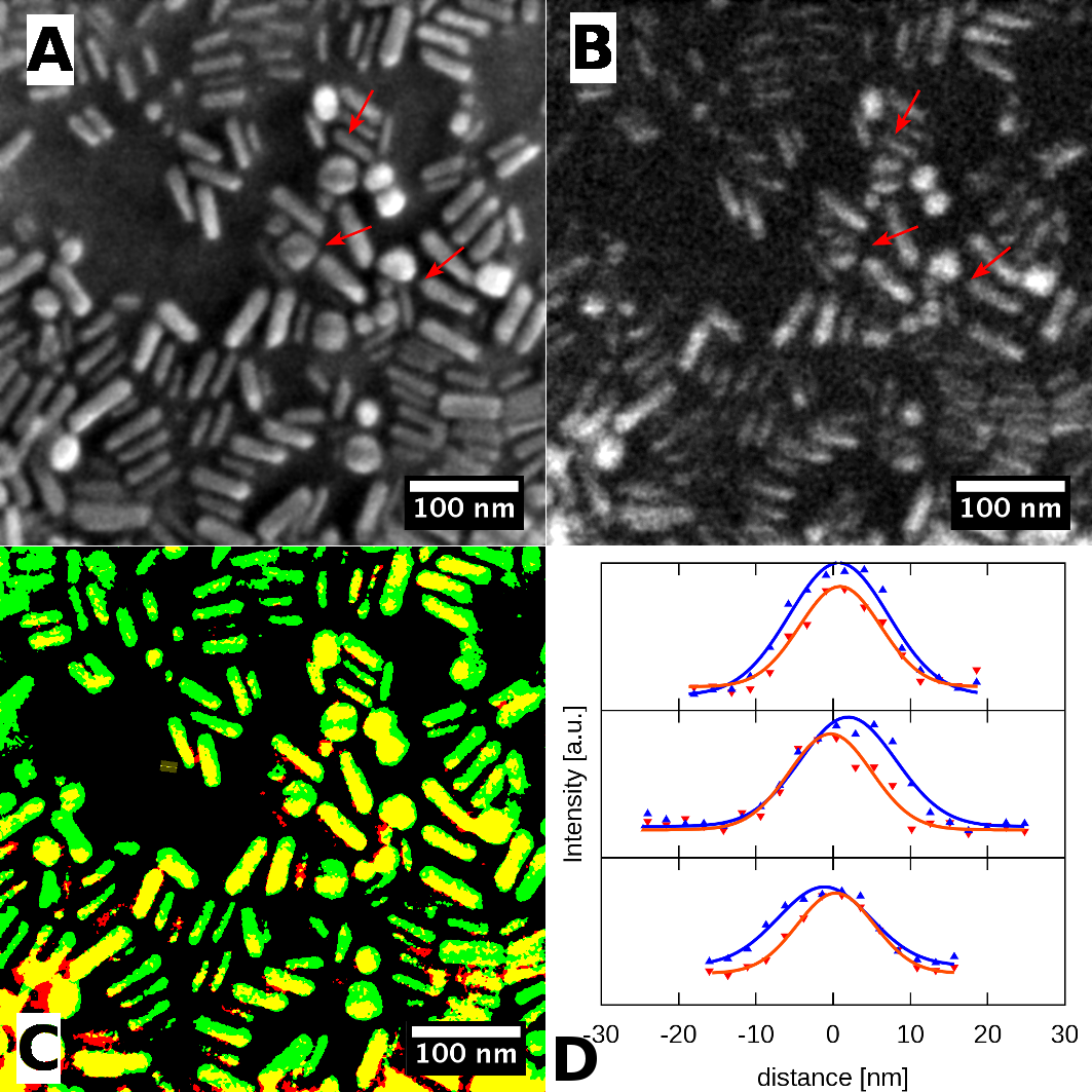
A length of 45 nm10 nm and a width 15 nm4 nm has been obtained from the secondary electron image presented in fig. 2(A). This results in an aspect ratio of 3 for these CTA covered rods. In fig. 2(B) the simultaneously recorded BSHe image is presented. The images have been recorded with an intermediate primary energy of only 20 keV to ensure an enhanced BSHe signal from the nano–rods. The energy of 20 keV has been specifically selected to increase the cross section for He scattering. Although lower energies would result in even higher BSHe yields, 20 keV is a good compromise between BSHe yield and SE as well as BSHe image resolution. Although the signal is still relatively weak the nano–rods appear slightly smaller in the BSHe image. A composite image—created using red and green for the SE and the BSHe signal, respectively—is presented in fig. 2(C). Several rods are visible showing a yellow core—a result of the compositing process between red and green—surrounded by a thin green border. This is a result of the CTA shell surrounding the gold nano–rods. The fact that the gold cores of the nano–rods are smaller than the nano–entities in SE mode is also evident from the three selected cross sections shown in fig. 2(D). The nano–rod diameters—obtained from Gaussian profiles—are listed in table 1.
| section | ⌀SE [nm] | ⌀BSHe [nm] |
|---|---|---|
| top | 12.4 | 10.6 |
| middle | 12.8 | 10.4 |
| bottom | 11.9 | 10.0 |
| average | 12.40.5 | 10.30.3 |
For comparison a similar area has been investigated using SEM at different voltages. In fig. 3 HRSEM images, colocalization analysis and cross sections are presented. The images have been recorded sequentially using 220 V and a current of 50 pA and 2000 V with a current of 200 pA for fig. 3(A) and 3(B), respectively.
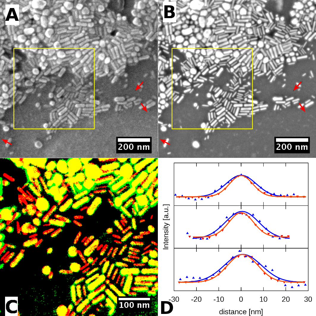
The difference between the low voltage (LV) image obtained at 220 V and the higher voltage (HV) image obtained at 2000 V is evident by comparing fig. 3(A) and 3(B). While in the latter the rods show a good signal to noise ratio and are clearly separated from each other as well as the background, this is not the case for the low voltage image. The thicker rods present in the composite image clearly show a yellow core surrounded by a green shell. This appearance is a consequence of the CTAB layer being visible only in the low voltage (green) channel but not in the higher voltage channel (red). The fact that some of the rods appear entirely red is due to the thresholding used when generating the composite image. The rods in question are in fact visible in the low voltage image but with a low signal to noise and consequently have been missed when creating the composite image. The fact that the rods are visualized to be thinner in the high energy image is also clear from the cross–sections presented in fig. 3(D). For all cross–sections the rod diameter is measured roughly 3 nm smaller in the 2000 V image (red in fig. 3(D)) as compared to the 220 V image (blue in fig. 3(D)). Table 2 summarizes the measured rod diameters for the selected cross–sections.
4 Discussion
From the results presented above it is clear that both methods can selectively visualize the gold core as well as the surrounding CTAB shell. In the next paragraphs we want to shed light on the underlying reasons and discuss the benefits of the different methods.
Helium Ion Microscopy is characterized by a high surface sensitivity in particular for thin carbon layers [14]. The small escape depth of secondary electrons (SE) generated by swift ions [21] results in the superior surface sensitivity and resolution [13] of the HIM SE image. This fact allows the detailed imaging of even very thin carbon layers, such as the CTAB layer in the present study. However, the availability of the simultaneously recorded backscattered helium (BSHe) image allows to also visualize the heavy gold cores. The difference in cross section and its Z2 dependence yields a high contrast between the gold cores and the carbon layer or the surrounding silicon substrate. From SRIM calculations, backscatter efficiencies of 0.05 and 0.02 for the CTA covered gold rods and the CTA covered silicon, respectively, are calculated. Using a detector opening angle of 245° and the given dose per pixel results in 6 BSHe atoms per pixel on the gold nano–rods and 2 BSHe atoms for the background. Despite the extremely small signal a contrast ratio of 3 is sufficient to confidently identify the gold rods. This contrast is enhanced further by utilizing the channeling into the underlying silicon substrate and so further suppressing the background signal.
Channeling is also observed in two different ways on some of the polycrystalline gold nano–particles. Firstly, different crystallographic orientations of the gold rods with respect to the incoming beam will result in varying amounts of backscattered helium. This gives rise to the different intensities between the various gold nano–rods in fig. 2(B). Secondly, channeling also reveals the polycrystalline nature of the nano–particles themselves. The effect is in particular visible for the round nano–particles at the end of the top most two cross–sections in fig. 2(B). Their coffee bean like appearance (brighter on the sides as compared to the darker middle) is most likely the result of twinning and thus different channeling conditions. Interestingly, the same contrast variation is observed in the SE image presented in fig. 2(B). Here, the contrast is a result of different CTA coverages for different crystallographic planes on the nano–particles [22].
By carefully comparing the cross–section of several nano–rods, the CTAB shell thickness could be determined. From the values presented in table 1 we calculate a minimum CTA shell thickness of 1.0 nm. This value is in excellent agreement with the expected thickness of 1.0 nm–1.5 nm [17] reported elsewhere. The shift between the SE (blue) and BSHe (red) signal is a result of the well known orientation dependence in SE images. This results in the pseudo topographic images also known from SEM. The detector is positioned in the top right corner relative to the image, resulting in an asymmetric rod profile. The BSHe detector—positioned in the beam path—does not suffer from this effect and yields a symmetric profile at the rod position. However, the actual shift is less than 10% of the rod diameter. It has to be pointed out that the shell thickness has to be taken into account when measuring the aspect ratio of such nano–rods. The CTA shell reduces the aspect ration from 4 to 3 due to the different relative contributions of the CTA shell to the length and width.
Modern scanning electron microscopes allow high resolution low voltage imaging in combination with a high surface sensitivity. By imaging the same area twice with different voltages one can selectively resolve the gold cores (HV) as well as the CTA shell (LV).
To better understand the difference between the two SEM imaging modes, Monte Carlo simulations using CASINO have been utilized. At least two effects can be identified which give rise to the difference between LV and HV SEM imaging. First, at low voltage the maximum penetration depth for electrons obtained from CASINO is 2.5 nm while at 2 kV the electrons easily pass through the rod into the underlying silicon substrate yielding a maximum penetration depth of up to 100 nm. However, BSE are not only loosing energy during the actual hard collision event but also on the way into the sample and when they return to the surface. At a primary energy of 220 eV the maximum escape depth of BSE—as calculated by CASINO—is 0.5 nm. As a consequence the gold core is completely invisible at 220 V, while at 2 kV a large portion of the signal stems from the embedded gold core. The effect is enhanced by a shift in the yields for SE and BSE as presented in table 3.
| signal | 0.22 kV | 2.0 kV |
|---|---|---|
| SE | 3.87 | 1.4 |
| BSE | 0.11 | 0.48 |
This shift results in the fact that at higher voltages the signal from the thin carbon layer diminishes in the huge contribution—composed of SE and BSE—from the gold core. The used in–lens detector allows for the efficient collection of these electrons at the small working distance used during measurement. It is the strong energy dependence of the SE as well as the BSE yields which is further enhanced by the choice of materials. Both contributions amplify the effect and allow the selective imaging of core and shell using different voltages.
5 Conclusion
We present a comparative investigation of CTAB layer thickness on gold nano–rods using HIM and SEM. Both methods can selectively image the gold core or the surrounding CTA shell. In HIM this is achieved by simultaneously recording the SE and BSHe signals. In SEM switching between ultra–low voltage and higher voltage imaging achieves the same result. Although the detector efficiencies in BSHe mode are extremely high and less than 10 backscattered helium atoms are sufficient to obtain a decent signal, the quality of the BSHe images is inferior to the high resolution HIM–SE images obtained from the CTAB layer. This is at least partially due to the UHV HIM equipment used. The base pressure of less than mbar ensures that thin carbon layers can be imaged over prolonged periods without adding new carbon as a result of cracking of hydrocarbons present in the sample chamber. In particular LV–SEM suffers from this problem and thin carbon layers are quickly deposited in the investigated area. On the other hand SEM has a faster sample turnover time and excels in the visualization of the gold cores. For the latter, carbon deposition is not an immediate problem and the definition of the rods is excellent allowing precision measurements of particle core length and width.
From both methods we estimated a CTAB layer thickness of 1.0 nm (HIM) – 1.5 nm (SEM). Both values are in excellent agreement with the expected thickness of 1.0 nm – 1.5 nm. Both methods arrive independently at values smaller than the full length of the CTA molecule. Deviations from the ideal double layer CTA structure can easily explain this discrepancy. Curled up molecules or an incomplete double layer coverage will result in a thinner effective CTA shell.
In summary, we have successfully measured the thickness of ultra–thin CTAB layers using HIM and SEM. However, while SEM excels in revealing the gold nano–rods, HIM is superior in the visualization of the CTAB layer.
Acknowledgements
This research is supported by the Dutch Technology Foundation STW, which is part of the Netherlands Organisation for Scientific Research (NWO), and which is partly funded by the Ministry of Economic Affairs.
References
- [1] W. Ahmed, E. S. Kooij, A. van Silfhout, B. Poelsema, Controlling the morphology of multi-branched gold nanoparticles., Nanotechnology 21 (12) (2010) 125605. doi:10.1088/0957-4484/21/12/125605.
- [2] S. E. Lohse, C. J. Murphy, The Quest for Shape Control: A History of Gold Nanorod Synthesis, Chemistry of Materials 25 (8) (2013) 1250–1261. doi:10.1021/cm303708p.
- [3] X. Ye, Y. Gao, J. Chen, D. C. Reifsnyder, C. Zheng, C. B. Murray, Seeded Growth of Monodisperse Gold Nanorods Using Bromide-Free Surfactant Mixtures., Nano lettersdoi:10.1021/nl400653s.
- [4] M. Grzelczak, J. Pérez-Juste, P. Mulvaney, L. M. Liz-Marzán, Shape control in gold nanoparticle synthesis., Chemical Society reviews 37 (9) (2008) 1783–91. doi:10.1039/b711490g.
- [5] B. Nikoobakht, M. A. El-Sayed, Preparation and Growth Mechanism of Gold Nanorods (NRs) Using Seed-Mediated Growth Method, Chemistry of Materials 15 (10) (2003) 1957–1962. doi:10.1021/cm020732l.
- [6] W. Ahmed, R. P. B. Laarman, C. Hellenthal, E. S. Kooij, A. van Silfhout, B. Poelsema, Dipole directed ring assembly of Ni-coated Au-nanorods., Chemical communications (Cambridge, England) 46 (36) (2010) 6711–3. doi:10.1039/c0cc01622e.
- [7] K. J. M. Bishop, C. E. Wilmer, S. Soh, B. a. Grzybowski, Nanoscale forces and their uses in self-assembly., Small 5 (14) (2009) 1600–30. doi:10.1002/smll.200900358.
- [8] E. C. Dreaden, A. M. Alkilany, X. Huang, C. J. Murphy, M. a. El-Sayed, The golden age: gold nanoparticles for biomedicine., Chemical Society reviews 41 (7) (2012) 2740–79. doi:10.1039/c1cs15237h.
- [9] N. J. Halas, Plasmonics: an emerging field fostered by Nano Letters., Nano letters 10 (10) (2010) 3816–22. doi:10.1021/nl1032342.
- [10] M. Chanana, L. M. Liz-Marzán, Coating matters: the influence of coating materials on the optical properties of gold nanoparticles, Nanophotonics 1 (3-4) (2012) 199–220. doi:10.1515/nanoph-2012-0008.
- [11] A. E. Vladár, M. T. Postek, B. Ming, On the Sub-Nanometer Resolution of Scanning Electron and Helium Ion Microscopes, Microscopy Today 17 (March) (2009) 6–13.
- [12] B. W. Ward, J. A. Notte, N. P. Economou, Helium ion microscope: A new tool for nanoscale microscopy and metrology, Journal of Vacuum Science & Technology B: Microelectronics and Nanometer Structures 24 (6) (2006) 2871. doi:10.1116/1.2357967.
- [13] R. Hill, F. Faridur Rahman, Advances in helium ion microscopy, Nuclear Instruments and Methods in Physics Research Section A: Accelerators, Spectrometers, Detectors and Associated Equipment 645 (1) (2011) 96–101. doi:10.1016/j.nima.2010.12.123.
- [14] G. Hlawacek, V. Veligura, S. Lorbek, T. F. Mocking, A. George, R. van Gastel, H. J. W. Zandvliet, B. Poelsema, Imaging ultra thin layers with helium ion microscopy: Utilizing the channeling contrast mechanism., Beilstein journal of nanotechnology 3 (2012) 507–12. doi:10.3762/bjnano.3.58.
- [15] D. Lau, A. E. Hughes, T. H. Muster, T. J. Davis, a. M. Glenn, Electron-beam-induced carbon contamination on silicon: characterization using Raman spectroscopy and atomic force microscopy., Microscopy and microanalysis : the official journal of Microscopy Society of America, Microbeam Analysis Society, Microscopical Society of Canada 16 (1) (2010) 13–20. doi:10.1017/S1431927609991206.
- [16] R. van Gastel, L. Barriss, C. Sanford, G. Hlawacek, L. Scipioni, A. Merkle, D. Voci, C. Fenner, H. J. W. Zandvliet, B. Poelsema, Design and performance of a Near Ultra High Vacuum Helium Ion Microscope, Microscopy and Microanalysis 17 (S2) (2011) 928–929. doi:10.1017/S1431927611005514.
- [17] Z. Sui, X. Chen, L. Wang, L. Xu, W. Zhuang, Y. Chai, C. Yang, Capping effect of CTAB on positively charged Ag nanoparticles, Physica E: Low-dimensional Systems and Nanostructures 33 (2) (2006) 308–314. doi:10.1016/j.physe.2006.03.151.
- [18] N. V. Venkataraman, S. Vasudevan, Hydrocarbon chain conformation in an intercalated surfactant monolayer and bilayer, Journal of Chemical Sciences 113 (5-6) (2001) 539–558. doi:10.1007/BF02708789.
- [19] H. Demers, N. Poirier-Demers, A. R. Couture, D. Joly, M. Guilmain, N. de Jonge, D. Drouin, Three-dimensional electron microscopy simulation with the CASINO Monte Carlo software., Scanning 33 (3) (2011) 135–46. doi:10.1002/sca.20262.
- [20] J. F. Ziegler, J. P. Biersack, M. D. Ziegler, SRIM, the stopping and range of ions in matter, SRIM Co., 2008.
- [21] R. Ramachandra, B. J. Griffin, D. C. Joy, A model of secondary electron imaging in the helium ion scanning microscope, Ultramicroscopy 109 (6) (2009) 748–757. doi:10.1016/j.ultramic.2009.01.013.
- [22] C. J. Johnson, E. Dujardin, S. a. Davis, C. J. Murphy, S. Mann, Growth and form of gold nanorods prepared by seed-mediated, surfactant-directed synthesis, Journal of Materials Chemistry 12 (6) (2002) 1765–1770. doi:10.1039/b200953f.