A micro-structured ion-implanted magnonic crystal
Abstract
We investigate spin-wave propagation in a microstructured magnonic-crystal waveguide fabricated by localized ion implantation. The irradiation caused a periodic variation in the saturation magnetization along the waveguide. As a consequence, the spin-wave transmission spectrum exhibits a set of frequency bands, where spin-wave propagation is suppressed. A weak modification of the saturation magnetization by is sufficient to decrease the spin-wave transmission in the band gaps by a factor of 10. These results evidence the applicability of localized ion implantation for the fabrication of efficient micron- and nano-sized magnonic crystals for magnon spintronic applications.
Magnonic crystals belong to the class of metamaterials and are artificially patterned magnetic media. This manufactured periodic pattern results in the formation of forbidden frequency bands for spin-wave excitations of the material.Sykes1976 ; Nikitov2001 The feasibility to store or process information by spin waves using a magnonic crystalChumak2010 ; Chumak2012 makes it a promising tool for magnon spintronic applications.Kruglyak2010 The future use in a chip-based spin-logic architecture, however, requires high-quality microscopic magnonic crystals that are easy to produce. Presently, they are realized in the form of microscopic waveguides with variable width,Chumak2009 arrays of coupled magnetic strips,Gubbiotti2007 ; Topp2010 antidot latticesLenk2012 and bicomponent magnonic crystals,Wang2009 ; Tacchi2012 all of which have proven as reliable methods. But there appear drawbacks like the formation of higher modes at the edge steps of the modulated sample topographyLee2009 ; Chumak2009 ; Ciubotaru2012 and the complicated fabrication procedures, respectively.
These problems can be overcome by patterning the magnetic properties of a waveguide without major changes of the sample topography by localized ion implantation.Volluet1981 ; Carter1982 ; Kaminsky2001 ; Barsukov2011 Irradiating a NiFe (permalloy) film with ions leads to a reduction of its saturation magnetization.Folks2003 ; Fassbender2006 ; Fassbender2006b Thus, localized ion implantation can be utilized to manipulate the spin-wave propagation by a pure magnetic patterning of a permalloy film.Obry2013
In this letter we present a one-dimensional micro-structured magnonic crystal waveguide with a periodic modulation of the saturation magnetization obtained by localized ion implantation. While the magnetic patterning method has nearly no impact on the waveguide topography, the change in the spin-wave propagation in the waveguide is drastic. A set of pronounced frequency band gaps exists in the spin-wave transmission spectrum, corresponding to a rejection of spin waves by the magnonic crystal. Furthermore, no scattering between different transversal waveguide modes occurs at the boundaries of the periodic pattern, as was also previously reported for other microscopically structured magnonic waveguides.Chumak2009 ; Lee2009 ; Ciubotaru2012

The experiments were performed on two NiFe waveguides (Fig. 1) with a width of m and a nominal thickness of nm, which were fabricated by means of conventional lift-off techniques and molecular beam evaporation. While one of the waveguides served as a reference waveguide, a periodic modulation in the saturation magnetization was imposed on the second waveguide by localized ion implantation. For this, a polymethyl methacrylate (PMMA) mask was patterned on top of the sample by e-beam lithography containing a set of m wide and nm long windows with a periodicity of m (inset of Fig. 1). The subsequent irradiation of the sample by a broad beam of Cr ions with a kinetic energy of keV and a fluence of ions/cm2 resulted in a decrease of in the unshielded regions to of its original value, as determined from polar magneto-optic Kerr effect measurementsMarko2010 on equally treated reference samples. Finally, a nm thick and nm wide Cu antenna was produced on top of the waveguides (Fig. 1). Applying a microwave current to the antenna, spin waves were excited in the NiFe waveguides by the dynamic Oersted field of the antenna, and they propagated perpendicularly to an external in-plane magnetic field mT (Damon-Eshbach geometry). The spin-wave intensity was detected using Brillouin light scattering (BLS) microscopy, which provides a high dynamic spectral range and a spatial resolution of nm.Demidov2004

The magnonic crystal character of the modulated waveguide becomes apparent in the measurement of the spin-wave transmission spectra (Fig. 2(a)). Here, the detected spin-wave intensity measured at a propagation distance of a few micrometers from the antenna has been plotted as a function of the microwave excitation frequency. For a better comparison, the spectra were normalized in intensity. With respect to the reference waveguide, the transmission spectrum of the magnonic crystal waveguide reveals two pronounced band gaps for spin-wave frequencies at GHz and at about GHz, where the spin-wave intensity drops by a factor of . These frequency regions constitute the rejection bands of the magnonic crystal.
Figure 2(b) displays the Damon-Eshbach type spin-wave dispersion relation, which was calculated according to Ref. Kalinikos1986, for a magnetic field of mT and a saturation magnetization of kA/m.parameters1 The latter value was determined from polar magneto-optic Kerr effect measurements on non-irradiated NiFe reference films, while the magnetic field value takes into account the demagnetizing fields originating at the waveguide edges.Demokritov2009 The dispersion relation reflects the characteristic features of the reference transmission spectrum. While the strong onset of spin-wave transmission at lower frequencies corresponds to the ferromagnetic resonance (FMR) frequency GHz, the gradual decrease in the detected spin-wave intensity towards higher frequencies can be understood by taking into account the finite size of the microwave antenna.Demidov2009 For the given antenna width of nm an efficient excitation of spin waves is restricted to spin waves up to a maximum wave vector of . According to Fig. 2(b), this results in an upper limit for the spin-wave frequency of GHz, which perfectly agrees with the observed values in the transmission spectrum of the reference waveguide (Fig. 2(a)).
Furthermore, for the transmission spectrum of the magnonic crystal waveguide, the positions of the frequency band gaps coincide with the first two resonance conditions for Bragg scattering from the periodic magnonic crystal pattern. The latter are indicated by the dotted lines in Fig. 2 and were calculated using the Bragg condition , which connects the spin-wave wave vector with the lattice constant m of the artificial lattice, where n is an integer number. It has to be noted that the waveguide thickness was used as a fitting parameter in the calculation of the spin-wave dispersion relation (Fig. 2(b)). While the thickness has basically no impact on the position of the FMR frequency, it strongly influences the frequency values for Bragg reflection. The resulting thickness value of nm reproduces the nominal thickness quite well. Since no capping layer was used on top of the NiFe, the oxidation of the waveguide surface and thus a reduction of the effective thickness is most likely.
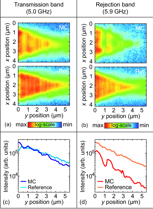
A more detailed analysis of the spin-wave propagation in the magnonic crystal waveguide was achieved by space-resolved BLS microscopy measurements (Fig. 3). Here, spatial maps of the spin-wave intensity distribution within the waveguides were taken for an excitation frequency in the transmission and rejection band, respectively. The investigated frequencies are indicated by the dashed lines in Fig. 2. Spin waves were excited by the antenna at m and detected locally by scanning the BLS laser focus across the waveguide. The detected spin-wave intensity is color-coded with red (blue) color representing high (low) intensity. In both cases the propagation in the magnonic crystal waveguide was compared to the propagation in the conventional reference waveguide.
For the excitation of spin waves in the transmission band with a frequency of GHz a weak difference in both intensity maps was observed (Fig. 3(a)). While in the reference waveguide the spin waves decay homogeneously with increasing distance from the antenna, a faster decay as well as a small overlaid oscillation in the intensity occurs in the magnonic crystal waveguide. Apparently, this is due to the implementation of the irradiated regions with a reduced and an increased Gilbert dampingFassbender2006 allowing for spin-wave reflection at the transitions between the irradiated and non-irradiated areas. A more quantitative analysis of the spin-wave decay along the waveguide is given in Fig. 3(c). Here, the total transmitted spin-wave intensity is shown as a function of the distance from the antenna, obtained by integrating the detected spin-wave signal over the position in Fig. 3(a). In the case of the reference waveguide the slope of this curve yields information about the spin-wave damping. However, for the magnonic crystal waveguide this is not trivial, since multiple reflections from the irradiated regions as well as the periodically modified saturation magnetization and damping have to be taken into account. In order to simplify the analysis, an effective decay length was used to quantify the transmission through the waveguide, i.e., to account for both damping and reflection losses. Fitting an exponential decay of the spin-wave intensity according to to the experimental data yielded values of m for the reference waveguide and m for the magnonic crystal waveguide (Fig. 3(c)). A small increase in by a factor of due to the irradiation was determined.
In contrast, the excitation of spin waves with a frequency of GHz, i.e., inside the band gap, has a notable impact on their propagation in the magnonic crystal waveguide. The intensity maps in Fig. 3(b) reveal a pronounced overlaid oscillation in the magnonic crystal waveguide being a sign of a standing spin-wave pattern due to the Bragg reflections from the artificial lattice. In addition, the decay of the transmitted intensity (Fig. 3(d)) in the magnonic crystal waveguide (m) was increased with respect to the reference waveguide (m) by a factor of . Beside the increased effective damping, the offset in intensity between both curves in Fig. 3(d) suggests that the excitation of spin waves in the magnonic crystal waveguide within the band gap has a lower efficiency. These observations give rise to the assumption that the suppression of spin waves by a factor of 10 in the rejection band is caused by two different effects: Partly, the effective spin-wave damping is increased due to Bragg scattering from the artificial crystal, but additionally the location of the antenna inside the magnonic crystal leads to a decreased excitation efficiency inside the rejection band.
In conclusion, localized ion implantation is a convenient method to fabricate high-performance magnonic crystal waveguides on the microscopic scale. A relatively weak, periodic change in the waveguide’s saturation magnetization of is sufficient for the formation of pronounced band gaps, where spin-wave propagation is efficiently suppressed. Since the waveguide consisted of one single, topographically unchanged material, spin waves with frequencies in the transmission bands were nearly unaffected. Hence, this class of magnonic crystal waveguides bears a high potential for future application in magnon spintronic devices.
The authors would like to thank the Nano Structuring Center (NSC) of the TU Kaiserslautern for support with the sample preparation and E. Papaioannou for the evaporation of the NiFe films. Financial support by the DFG (SE-1771/1-2) is gratefully acknowledged.
References
- (1) C. G. Sykes. J. D. Adam, and J. H. Collins, Appl. Phys. Lett. 29, 388 (1976).
- (2) S. A. Nikitov, Ph. Tailhades, and C. S. Tsai, J. Magn. Magn. Mater. 236, 320 (2001).
- (3) A. V. Chumak, A. N. Slavin, V. S. Tiberkevich, A. D. Karenowska, A. A. Serga, J. F. Gregg, and B. Hillebrands, Nature Commun. 1, 141 (2010).
- (4) A. V. Chumak, V. I. Vasyuchka, A. A. Serga, M. P. Kostylev, V. S. Tiberkevich, and B. Hillebrands, Phys. Rev. Lett. 108, 257207 (2012).
- (5) V. V. Kruglyak, S. O. Demokritov, and D. Grundler, J. Phys. D 43, 264001 (2010).
- (6) A. V. Chumak, P. Pirro, A. A. Serga, M. P. Kostylev, R. L. Stamps, H. Schultheiss, K. Vogt, S. J. Hermsdoerfer, B. Laegel, P. A. Beck, and B. Hillebrands, Appl. Phys. Lett. 95, 262508 (2009).
- (7) G. Gubbiotti, S. Tacchi, G. Carlotti, N. Singh, S. Goolaup, A. O. Adeyeye, and M. Kostylev, Appl. Phys. Lett. 90, 092503 (2007).
- (8) J. Topp, D. Heitmann, M. P. Kostylev, and D. Grundler, Phys. Rev. Lett. 104, 207205 (2010).
- (9) B. Lenk, N. Abeling, J. Panke, and M. Münzenberg, J. Appl. Phys. 112, 083921 (2012).
- (10) Z. K. Wang, V. L. Zhang, H. S. Lim, S. C. Ng, M. H. Kuok, S. Jain, and A. O. Adeyeye, Appl. Phys. Lett. 94, 083112 (2009).
- (11) S. Tacchi, G. Duerr, J. W. Klos, M. Madami, S. Neusser, G. Gubbiotti, G. Carlotti, M. Krawczyk, and D. Grundler, Phys. Rev. Lett. 109, 137202 (2012).
- (12) K.-S. Lee, D.-S. Han, and S.-K. Kim, Phys. Rev. Lett. 102, 127202 (2009).
- (13) F. Ciubotaru, A. V. Chumak, N. Yu. Grigoryeva, A. A. Serga, and B. Hillebrands, J. Phys. D 45, 255002 (2012).
- (14) G. Volluet and P. Hartemann, Proc. IEEE Ultrasonics Symp., 394 (1981).
- (15) R. L. Carter, J. M. Owens, C. V. Smith, and K. W. Reed, J. Appl. Phys. 53, 2655 (1982).
- (16) W. M. Kaminsky, G. A. C. Jones, N. K. Patel, W. E. Booij, M. G. Blamire, S. M. Gardiner, Y. B. Xu, and J. A. C. Bland, Appl. Phys. Lett. 78, 1589 (2001).
- (17) I. Barsukov, F. M. Römer, R. Meckenstock, K. Lenz, J. Lindner, S. Hemken to Krax, A. Banholzer, M. Körner, J. Grebing, J. Fassbender, and M. Farle, Phys. Rev. B 84, 140410(R) (2011).
- (18) L. Folks, R. E. Fontana, B. A. Gurney, J. R. Childress, S. Maat, J. A. Katine, J. E. E. Baglin, and A. J. Kellock, J. Phys. D 36, 2601 (2003).
- (19) J. Fassbender, J. von Borany, A. Mücklich, K. Potzger, W. Möller, J. McCord, L. Schultz, and R. Mattheis, Phys. Rev. B 73, 184410 (2006).
- (20) J. Fassbender and J. McCord, Appl. Phys. Lett. 88, 252501 (2006).
- (21) B. Obry, T. Meyer, P. Pirro, T. Brächer, B. Lägel, J. Osten, T. Strache, J. Fassbender, and B. Hillebrands, Appl. Phys. Lett. 102, 022409 (2013).
- (22) D. Markó, T. Strache, K. Lenz, J. Fassbender, and R. Kaltofen, Appl. Phys. Lett. 96, 022503 (2010).
- (23) V. E. Demidov, S. O. Demokritov, B. Hillebrands, M. Laufenberg, and P. P. Freitas, Appl. Phys. Lett. 85, 2866 (2004).
- (24) B. A. Kalinikos and A. N. Slavin, J. Phys. C: Solid State Phys. 19, 7013 (1986).
- (25) Further assuming a NiFe waveguide with thickness nm and width m, a gyromagnetic ratio GHz/T, and an exchange stiffness constant J/m.
- (26) S. O. Demokritov and V. E. Demidov, in Spin Wave Confinement, edited by S. O. Demokritov (Pan Stanford Publishing Pte. Ltd., Singapore, 2009), Chap. 1.
- (27) V. E. Demidov, M. P. Kostylev, K. Rott, P. Krzysteczko, and G. Reiss, and S. O. Demokritov, Appl. Phys. Lett. 95, 112509 (2009).