A ballistic junction in suspended graphene with split bottom gates
Abstract
We have developed a process to fabricate suspended graphene devices with local bottom gates, and tested it by realizing electrostatically controlled junctions on a suspended graphene mono-layer nearly 2 m long. Measurements as a function of gate voltage, magnetic field, bias, and temperature exhibit characteristic Fabry-Perot oscillations in the cavities formed by the junction and each of the contacts, with transport occurring in the ballistic regime. Our results demonstrate the possibility to achieve a high degree of control on the local electronic properties of ultra-clean suspended graphene layers, a key aspect for the realization of new graphene nanostructures.
pacs:
73.63.-b, 72.80.Vp, 73.40.-c, 07.60.LyTechnical developments in device fabrication are essential to perform transport experiments revealing the intrinsic electronic properties of graphene. Suspended graphene devices Bolotin et al. (2008); Du et al. (2008) and devices with hexagonal boron nitride (hBN) as supporting substrate Dean et al. (2010, 2012) provide clear examples. The same is true for double-gated devices, in which graphene is not in direct contact with any dielectric material. Weitz et al. (2010); Velasco et al. (2012); Allen, Martin, and Yacoby (2012) Indeed, these devices have allowed the observation of phenomena such as the fractional quantum Hall effect, Du et al. (2009); Bolotin et al. (2009); Dean et al. (2011); Ki, Fal’ko, and Morpurgo (2013) new interaction-induced symmetry broken states in bilayers, Weitz et al. (2010); Velasco et al. (2012) and manifestations of ballistic transport. Mayorov et al. (2011); Campos et al. (2012); Ki and Morpurgo (2013) Even more advanced experiments would be possible if double-gating on suspended devices could be performed locally. In bilayer graphene, for instance, local double gating would allow the study of topological confinement, Martin, Blanter, and Morpurgo (2008) and the realization of fully electrostatically tunable junctions, of interest to generate or detect light at continuously tunable frequencies in the THz to mid infrared range. As an essential step towards the realization of these new structures, here we describe a technique to fabricate high-quality suspended graphene devices with local bottom gates and apply it to the realization of an electrostatically tunable, ballistic junction in monolayer graphene.
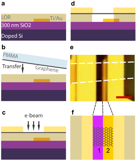
The fabrication process is illustrated schematically in Fig. 1. The first step consists in preparing the bottom gates in the desired configuration –in the present case, a simple single strip– on a doped silicon substrate covered with 300 nm SiO2, by using conventional techniques (electron-beam lithography, Ti/Au evaporation, and lift-off). Next, a 450-nm-thick layer of polydimethylglutarimide (PMGI)-based lift-off resist (LOR, MicroChem) is spun onto the substrate (Fig. 1(a)). LOR resist is chosen because it is not only compatible with all subsequent micro-fabrication processes, but also it can be exposed with an electron beam and developed away to suspend graphene at the end of the fabrication process. Tombros et al. (2011a, b); Ki and Morpurgo (2012)
As a second step, a graphene flake is transferred onto the LOR layer, and positioned on to the bottom gate (Fig. 1(b)). To this end, we adapted a technique developed to fabricate graphene/hBN heterostructures. Dean et al. (2010) Specifically, graphene is exfoliated using an adhesive tape and placed on a different substrate, previously coated with a layer of water soluble polymer (a 9 wt. poly(4-styrenesulfonic acid) solution in water) and a layer of PMMA. Nam et al. (2011) After the desired flake is identified under an optical microscope, the substrate is immersed in water, causing the water-soluble polymer to dissolve and the PMMA to float. The floating PMMA is retrieved using a plastic support, which is then mounted onto a micro-manipulator under an optical microscope. This enables the graphene flake to be transferred onto the LOR, aligned to the bottom gate with a precision of a few microns (Fig. 1(b)). After securing it by heating at 105 for 40 minutes, the flake is contacted with Ti/Au electrodes (10/60 nm thick) defined by conventional electron-beam lithography, metal evaporation, and lift-off (for PMMA on LOR, development and lift-off are done using Xylene, Tombros et al. (2011a, b); Ki and Morpurgo (2012) at room temperature and 90 , respectively). In the final step, the LOR under the graphene layer is exposed with an electron beam (Fig. 1(c)) and developed away to achieve the suspension (Fig. 1(d)). Tombros et al. (2011a, b); Ki and Morpurgo (2012)


We have applied this technique to suspend a 1.8 m long graphene monolayer over a bottom gate that overlaps with about half of the suspended length (see Fig. 1(e)). By screening the potential generated by a voltage applied to the conducting Si substrate, the bottom gate defines two regions (1 and 2, see Fig. 1(f)), whose carrier density and type can be controlled by applying voltages to the doped silicon substrate () and to the local gate itself (). Transport measurements as a function of and were performed in a Heliox He3 system to characterize the device at different magnetic field (), bias (), and temperature (). Prior to the measurements, the device was annealed at 4.2 K by passing a sufficiently large current through the graphene flake.
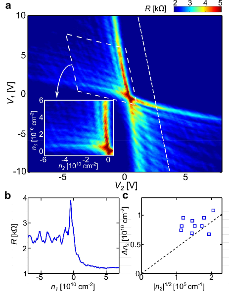
Fig. 2(a) shows the resistance measured at K as a function of and . Four quadrants can be identified, roughly corresponding to and having the same or opposite sign. When the sign is the same, no junction is present in the device: only either electrons or holes are accumulated in regions 1 and 2. A junction is present between region 1 and 2 when and have opposite sign. The borders of the different quadrants are not parallel to the and axis, because of the cross-talk between two gates: does not only change the density in region 1 () but also –to a lesser extent– the density in region 2 (); similarly, also influences the density . Although, in general, that the density is not spatially uniform in regions 1 and 2 (this is obvious when a junction is present, in which case the carrier density vanishes at the interface between the two regions), accounting as much as possible for the effect of the cross-talk is useful to analyze the data. This can be done by looking at the gate and magnetic field dependence of the quantized Hall conductance plateaus in the unipolar regime, where (i.e., when the density non uniformity is less pronounced). We find [1010 cm-2] [V] + [V] + 0.5 and [1010 cm-2] [V] + [V] 0.4 (the constants account for the shift of charge neutrality point from V; the proportionality terms between and are in good agreement with the estimated geometrical capacitances). The resistance as a function of and defined in this way is shown in the inset of Fig. 2(a).


When and are biased with opposite polarity to create a junction, the resistance doubles as compared to when no junction is present (compare, e.g., the resistance for and in Fig. 2(b)). This shows that the junction gives a large contribution to the total device resistance, despite the sizable device length (1.8 m in total). In particular, the junction contribution significantly larger as compared to previously studied and junctions on SiO2 substrates. Huard et al. (2007); Williams, Dicarlo, and Marcus (2007); Gorbachev et al. (2008); Stander, Huard, and Goldhaber-Gordon (2009)
Fig. 2(a) further shows that the resistance also oscillates as a function of and when a junction is formed, in a way resembling the behavior of graphene junctions on a Si/SiO2 substrate. Young and Kim (2009); Nam et al. (2011) In that case, the oscillations were shown to originate from Fabry-Perot interference of Dirac electrons moving ballistically within the ( nm long) cavity defined by the region. Young and Kim (2009); Nam et al. (2011); Shytov, Rudner, and Levitov (2008) In our device, Fabry-Perot oscillations occur in cavities formed by the junction and each of the two interfaces with the metal contacts, where carriers are also backscattered. Miao et al. (2007); Cho and Fuhrer (2011) Our device therefore consists of two Fabry-Perot cavities connected in series, and the ”checkerboard” pattern visible in Fig. 2(a) is a manifestation of interference in both cavities. The clear visibility of the oscillations directly in the resistance (Figs. 2(a) and 2(b)), without the need of derivating the data, is indicative of the high quality of the suspended junction. Young and Kim (2009); Nam et al. (2011)
An estimate of the oscillation period (i.e., the distance in density between two nearest resistance peaks or dips) is obtained by imposing that the dynamical phase acquired by an electron wave propagating back and forth in the cavity is equal to , i.e. (the subscript label the region). As , we obtain (note that several previous references Young and Kim (2009); Nam et al. (2011); Velasco et al. (2009) reported an incorrect expression, , differing by a factor of 2 from ours). The dotted line in Fig. 2(c) represents the values of estimated using this formula for region 2 ( nm), and the open squares are the experimental values extracted from the most pronounced oscillations measured upon changing (a similar result is obtained for region 1). The order of magnitude and the trend in the data are well captured by the simple theoretical expression. The experimental values, however, are somewhat larger than expected, because the carrier density in the region close to the junction is lower than the calculated value . The lower density causes a smaller value of , and therefore a smaller phase shift and an additional increase in carrier density is needed to compensate for this effect.
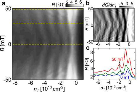
The evolution of the oscillation phase upon increasing magnetic field (see Fig. 3) provides further evidence for the Fabry-Perot nature of the interference. Shytov, Rudner, and Levitov (2008); Young and Kim (2009); Nam et al. (2011) Fig. 3(a) shows the -dependence of the oscillations upon changing at fixed cm-2 (i.e., by changing and along the dashed line depicted in Fig. 2(a)), which exhibits a phase shift at -30 mT (varying at fixed gives comparable results). Fig. 3(b) shows the same effect in the derivative of the conductance () with respect to , and panel (c) illustrates the occurrence of the phase shift, with three individual slices of the color plot shown in (a), taken at 30, and 50 mT.
As discussed for junctions, Shytov, Rudner, and Levitov (2008); Nam et al. (2011); Young and Kim (2009) the phase shift originates from the unique properties of Dirac electrons, namely the angular dependence of the reflection probability at a junction, Katsnelson, Novoselov, and Geim (2006); Cheianov and Fal’ko (2006) and the accumulation of a Berry phase along momentum-space trajectories that enclose the origin. Novoselov et al. (2005); Zhang et al. (2005) For a given position of the Fermi energy, the electrons contributing predominantly to the Fabry-Perot resistance oscillations are those incident on the junction with a certain transverse momentum (; the specific value depends on the density profile across the junction). Shytov, Rudner, and Levitov (2008); Young and Kim (2009) Upon increasing the perpendicular magnetic field, the electron trajectories in the Fabry-Perot cavity are bent, and –in momentum space– they eventually enclose the origin. Young and Kim (2009); Shytov, Rudner, and Levitov (2008) When this happens, an additional Berry phase is acquired, causing the phase shift in the resistance oscillations. For nm long junctions on substrate, the shift was found to occur at -500 mT. Young and Kim (2009); Nam et al. (2011) Assuming a comparable value of (within a factor of 2-3), this is consistent with our observations: the phase shift occurs at an order of magnitude smaller -30 mT, corresponding to an order of magnitude longer cavity.
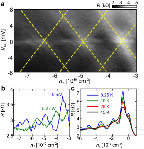
Finally, we discuss the characteristic energy scale of the resistance oscillations. Fig. 4(a) shows the differential resistance measured as a function of bias and density . Systematically, the position of the resistance peaks shifts linearly upon increasing , as expected for Fabry-Perot interference. Miao et al. (2007); Cho and Fuhrer (2011) The shift is also illustrated by Fig. 4(b), which compares measurements taken at and mV. From both Figs. 4(a) and 4(b), the bias needed to shift a maximum of differential resistance into a minimum is approximately 5 meV. We have also looked at the energy dependence of the oscillation by changing temperature, and found that the oscillations are washed out at about 40 K ( meV). Since, owing to the non-uniform charge density, the level spacing in the cavity is somewhat larger than the particle-in-a-box value meV (with m and m/s), the energy scale found in the experiments is consistent with the simplest theoretical estimate.
We conclude that the behavior of our device is consistent with the presence of a junction, and with transport occurring in the ballistic regime over a length comparable to the device size (1.8 m). The measurements therefore confirm that the fabrication technique that enables the realization of suspended graphene devices with local bottom gates preserves the high quality of the material. In the future, this technology will be applied to realize new graphene devices relying on the local control of the electrostatic potential and electric field, such as the nano-structures needed for the study of Veselago lensing, Cheianov, Fal’ko, and Altshuler (2007) of collimation of electrons, Park et al. (2008) and of topological confinement. Martin, Blanter, and Morpurgo (2008)
We gratefully acknowledge A. Ferreira for technical support and financial support from the SNF, NCCR MaNEP, and NCCR QSIT.
References
- Bolotin et al. (2008) K. Bolotin, K. J. Sikes, Z. Jiang, M. Klima, G. Fudenberg, J. Hone, P. Kim, and H. L. Stormer, Solid State Communications 146, 351 (2008).
- Du et al. (2008) X. Du, I. Skachko, B. A., and E. Y. Andrei, Nature Nanotechnology 3, 491 (2008).
- Dean et al. (2010) C. R. Dean, A. F. Young, I. Meric, C. Lee, L. Wang, S. Sorgenfrei, K. Watanabe, T. Taniguchi, P. Kim, K. L. Shepard, and J. Hone, Nature Nanotechnology 5 (2010).
- Dean et al. (2012) C. Dean, A. Young, L. Wang, I. Meric, G.-H. Lee, K. Watanabe, T. Taniguchi, K. Shepard, P. Kim, and J. Hone, Solid State Communications 152, 1275 (2012).
- Weitz et al. (2010) R. T. Weitz, M. T. Allen, B. E. Feldman, J. Martin, and A. Yacoby, Science 330, 812 (2010).
- Velasco et al. (2012) J. Velasco, L. Jing, W. Bao, Y. Lee, P. Kratz, V. Aji, M. Bockrath, C. N. Lau, C. Varma, R. Stillwell, D. Smirnov, F. Zhang, J. Jung, and A. H. MacDonald, Nature Nanotechnology 7, 156 (2012).
- Allen, Martin, and Yacoby (2012) M. T. Allen, J. Martin, and A. Yacoby, Nature Communications 3, 934 (2012).
- Du et al. (2009) X. Du, I. Skachko, F. Duerr, A. Luican, and E. Y. Andrei, Nature 462, 192 (2009).
- Bolotin et al. (2009) K. I. Bolotin, F. Ghahari, M. D. Shulman, H. L. Stormer, and P. Kim, Nature 462, 196 (2009).
- Dean et al. (2011) C. R. Dean, A. F. Young, P. Cadden-Zimansky, L. Wang, H. Ren, K. Watanabe, T. Taniguchi, P. Kim, J. Hone, and K. L. Shepard, Nature Physics 7, 693 (2011).
- Ki, Fal’ko, and Morpurgo (2013) D.-K. Ki, V. I. Fal’ko, and A. F. Morpurgo, Submitted (2013).
- Mayorov et al. (2011) A. S. Mayorov, R. V. Gorbachev, S. V. Morozov, L. Britnell, R. Jalil, L. A. Ponomarenko, P. Blake, K. S. Novoselov, K. Watanabe, T. Taniguchi, and A. K. Geim, Nano Letters 11, 2396 (2011).
- Campos et al. (2012) L. Campos, A. Young, K. Surakitbovorn, K. Watanabe, T. Taniguchi, and P. Jarillo-Herrero, Nature Communications 3 (2012).
- Ki and Morpurgo (2013) D.-K. Ki and A. F. Morpurgo, In preparation (2013).
- Martin, Blanter, and Morpurgo (2008) I. Martin, Y. M. Blanter, and A. F. Morpurgo, Physical Review Letters 100, 036804 (2008).
- Tombros et al. (2011a) N. Tombros, A. Veligura, J. Junesch, J. J. van den Berg, P. J. Zomer, M. Wojtaszek, I. J. Vera-Marun, H. T. Jonkman, and B. J. van Wees, Journal of Applied Physics 109 (2011a).
- Tombros et al. (2011b) N. Tombros, A. Veligura, J. Junesch, M. H. D. Guimar es, I. J. Vera-Marun, H. T. Jonkman, and B. J. van Wees, Nature Physics 7, 697 (2011b).
- Ki and Morpurgo (2012) D.-K. Ki and A. F. Morpurgo, Physical Review Letters 108, 266601 (2012).
- Nam et al. (2011) S.-G. Nam, D.-K. Ki, J. W. Park, Y. Kim, J. S. Kim, and H.-J. Lee, Nanotechnology 22, 415203 (2011).
- Huard et al. (2007) B. Huard, J. Sulpizio, N. Stander, K. Todd, B. Yang, and D. Goldhaber-Gordon, Physical Review Letters 98, 8 (2007).
- Williams, Dicarlo, and Marcus (2007) J. R. Williams, L. Dicarlo, and C. M. Marcus, Science 317, 638 (2007).
- Gorbachev et al. (2008) R. V. Gorbachev, A. S. Mayorov, A. K. Savchenko, D. W. Horsell, and F. Guinea, Nano letters 8, 1995 (2008).
- Stander, Huard, and Goldhaber-Gordon (2009) N. Stander, B. Huard, and D. Goldhaber-Gordon, Physical Review Letters 102, 1 (2009).
- Young and Kim (2009) A. F. Young and P. Kim, Nature Physics 5, 222 (2009).
- Shytov, Rudner, and Levitov (2008) A. Shytov, M. Rudner, and L. Levitov, Physical Review Letters 101, 10 (2008).
- Miao et al. (2007) F. Miao, S. Wijeratne, Y. Zhang, U. C. Coskun, W. Bao, and C. N. Lau, Science 317, 1530 (2007).
- Cho and Fuhrer (2011) S. Cho and M. Fuhrer, Nano Research 4, 385 (2011).
- Velasco et al. (2009) J. Velasco, G. Liu, W. Bao, and C. Ning Lau, New Journal of Physics 11, 095008 (2009).
- Katsnelson, Novoselov, and Geim (2006) M. I. Katsnelson, K. S. Novoselov, and A. K. Geim, Nature Physics 2, 620 (2006).
- Cheianov and Fal’ko (2006) V. Cheianov and V. Fal’ko, Physical Review B 74, 1 (2006).
- Novoselov et al. (2005) K. S. Novoselov, A. K. Geim, S. V. Morozov, D. Jiang, M. I. Katsnelson, I. V. Grigorieva, S. V. Dubonos, and A. A. Firsov, Nature 438, 197 (2005).
- Zhang et al. (2005) Y. Zhang, Y.-W. Tan, H. L. Stormer, and P. Kim, Nature 438, 201 (2005).
- Cheianov, Fal’ko, and Altshuler (2007) V. V. Cheianov, V. Fal’ko, and B. L. Altshuler, Science 315, 1252 (2007).
- Park et al. (2008) C.-H. Park, Y.-W. Son, L. Yang, M. L. Cohen, and S. G. Louie, Nano Letters 8, 2920 (2008).