Characterization of the JUDIDT Readout Electronics for Neutron Detection
R. Fabbria,b, U. Clemensa,
R. Engelsa, G. Kemmerlinga, and S. van Waasena
a Forschungszentrum Jülich (FZJ), Jülich
b Corresponding Author: r.fabbri@fz-juelich.de
Abstract
The Group for the development of neutron and gamma detectors in the Central Institute of Engineering, Electronics and Analytics (ZEA-2) at Forschungszentrum Jülich (FZJ) has developed, in collaboration with European institutes, an Anger Camera prototype for improving the impact point reconstruction of neutron tracks. The detector is a chamber filled with + gas for neutron capture and subsequent production of a tritium and a proton. The energy deposition by the ions gives rise to drifting electrons with an avalanche amplification as they approach a micro-strip anode structure. The scintillating light, generated during the electron drift and avalanche stage, is collected by four vacuum photomultipliers. The position reconstruction is performed via software algorithms. The JUDIDT readout electronics was modified at ZEA-2 to cope with the data acquisition requirements of the prototype. The results of the commissioning of the electronics are here presented and commented.
Forschungszentrum Jülich
Internal Report No. FZJ_2013_02194
1 Introduction
At current and future neutron facilities, like the research reactor FRM-II [1], or the European Spallation Source ESS [2], Small Angle Neutron Scattering (SANS) will obtain a major improvement by the much higher neutron fluxes than previously delivered. This leads to an intensity gain of at least one order of magnitude for SANS instruments, allowing a more detailed study of complex structures and fast processes. To cope with these expected high intensities the new detector readout system system JUDIDT [3] was developed for the SANS-diffractometer KWS1 at the previously active research reactor FRJ-2 of the Forschungszentrum Júlich, Germany. The system was then modified for a later use at the KWS2 experiment at FRM-II.
Within the FP7/NMI3 [4] European-founded project it was proposed to use the JUDIDT readout electronics for the data acquisition of a novel Anger Camera prototype [5], being able to cope with counting rates of several hundred kilohertz. Some modifications were implemented to properly handle the signal generated by the scintillating light in the volume gas. The proposed prototype underwent a full series of measurements at several neutron test-beam facilities in Europe, showing the capability to cope with the high demanding performance [5].
In this paper the results of the characterization of the stand-alone electronics are presented and commented. In addition, the data acquisition with the entire system detector plus the JUDIDT readout system will be described and the corresponding results discussed.
2 JUDIDT Electronics: Description and Properties
To cope with the high rates provided by the modern neutron beam facilities, the ZEA-2 Institute at FZJ, has developed the readout system JUDIDT (Jülicher Digitales Detektor Auslesssystem). The design of the electronics comprises a fast signal and data processing by usage of modern technologies like field-programmable gate arrays (FPGAs).
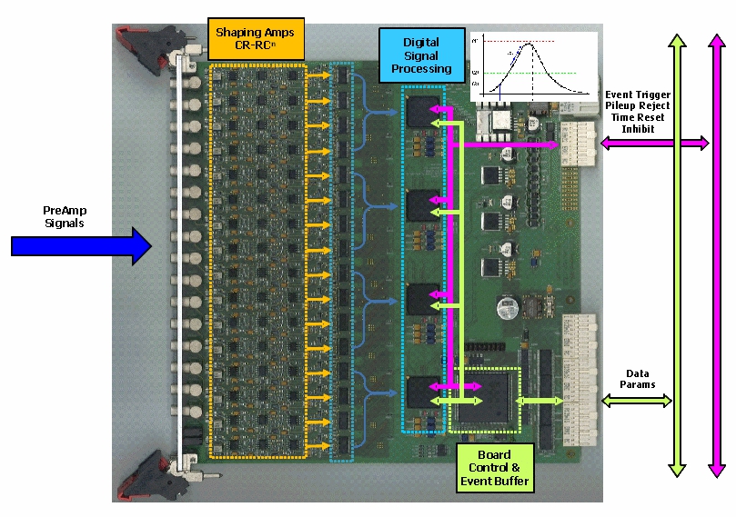
A detailed description of the electronics can be found in [3]. Here we address only its main features: the front-head is equipped with LEMO Ohm connectors to handle up to pre-amplified signals. According to the selected capacitor on the integrator stage the amplifier, different gain can be obtained. The signal leaves the main amplification and shaping stage with a decay time typically of ns, and is then feeded to its dedicated 12-bit ADC in the board, Fig. 1. Each FPGA handles four input channels and stores in a circular buffer the values provided by the individual ADCs, which sample their corresponding signal at a rate of MHz (every ns). As soon as a maximum in one channel is found, then the amplitude is evaluated also for the other channels in a selectable time window enclosing the measured peaking time. In the main FPGA register several cuts can be set to select events in specific amplitude and time windows. The setting of the FPGA is performed via API functions provided by the driver developers.
The bit ADC (AD9236) covers an amplitude range from zero up to two Volts with an ADC resolution of mV per ADC unit. The data in the upper half of the ADC dynamic range ( bits) are then shipped to an external computer through a GByte optical link using only bits, thus deteriorating the signal resolution down to mV. Considering that the main amplification stage is configured to provide a gain factor of ten results an overall resolution measured by the analyzer of mV per ADC unit.
3 Test-Bench Description
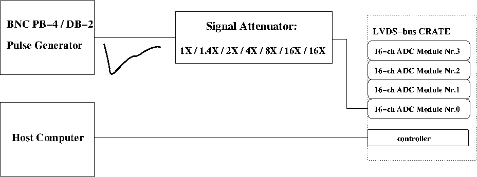
The characterization measurements of the JUDIDT electronics were performed at the laboratories in ZEA-2, The typical setup of the test-bench is shown in Fig. 2. An analogue voltage generator (BNC by Berkeley Nucleonics Corp.) provides a tailed pulse with negative polarity for different selectable values of pulse rate and with variable amplitude. Additionally, a device by Tennelec was used to provide selectable attenuator factors to the voltage tailed signal.
The attenuated signal is then injected in one of the input channels of the investigated board, and the processed output signal (e.g., the measured peaking amplitude) is saved in a binary file on hard disk, using the dedicated data acquisition software developed for the laboratory [6]. The data acquisition is driven from a Windows XP machine connected to the LVDS-bus based crate (develped at ZEA-2) via a SIS1100 Gbit optical link interface on both sides of the link. The DAQ can be easily ported to a LINUX system, being the software cross-platform build. The electronics performance has been also investigated using it as readout system for the Anger Camera Prototype [5], using neutron sources in the ZEA-2 laboratory.
4 Electrical Noise Investigation
The readout system has a very low intrinsic noise. Due to this optimal feature the pedestal distribution in each channel appears like a delta function at one or seldomly two ADC units. In this scenario it is difficult to reliably estimate the system noise as the root mean squared of the pedestal distribution.
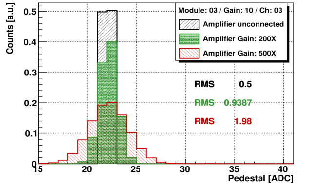
A possible solution is to couple one input channel to the negative unipolar output of an amplifier. Here, we have used the amplifier ORTEC . Different gain factors were applied in order to make the pedestal distribution broader, thus covering as many ADC channels as possible. It is clear that while coupling an amplifier to the readout electronics the measured noise is somehow the convolution of the noise arising from both systems, and can likely provide only an upper limit estimation.
An example of our procedure is presented in Fig. 3, where the pedestal of the same channel is shown in different configurations for the amplifier. At the largest gain used, the distribution is well Gaussian and covers many ADC channels, with a spread of 1.98 ADC units, resulting in a negligible noise level.
5 Pedestal Uniformity and Adjustment
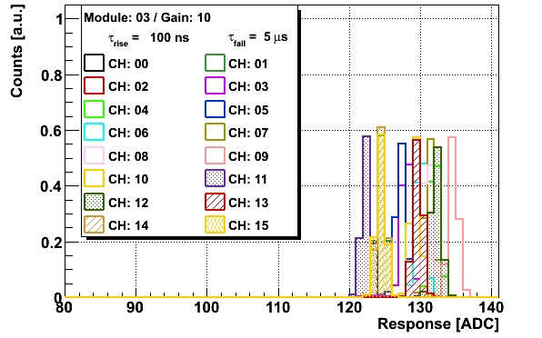
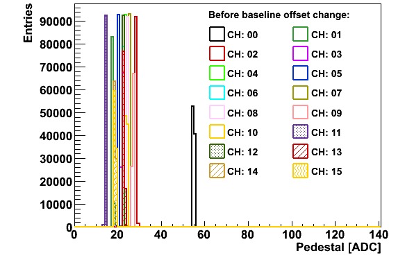
The peaking amplitude of the input signal can be measured differently by the independent channels of a board. This effect is due by the different intrinsic pedestal offset of each channel, and by a possible gain mismatch of the individual amplification channels. An example of this bias is shown in Fig. 4, resulting in an effective covered dynamic range not equivalent for all the ADC channels.
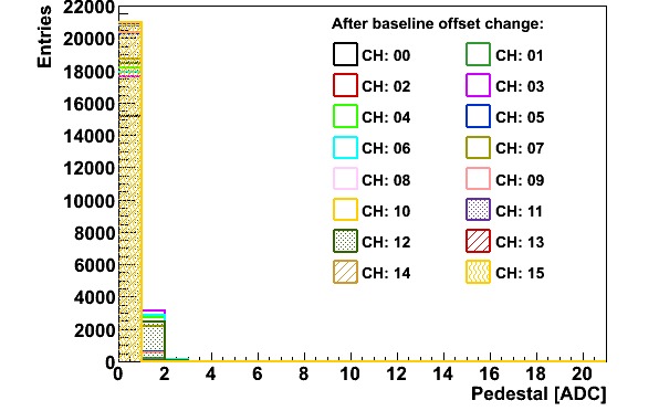
This feature can be cured by changing the baseline offset which can be modified by the data acquisition software tuning the DAC at the end of the amplifying stage, Fig. 1. The effect of the baseline correction is presented in Fig. 5. The gain mismatch in the amplifying stage and/or in the voltage setting of the photomultiplier can be recovered instead by gain-matching procedures, as the technique described in Sec. 10.
It is clear that by following this procedure the entire ADC range can be covered by all input channels, avoiding artificial bias in the measurements.
6 Cross-Talk between Input Channels
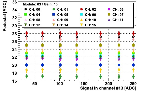
In a multi-channel readout system it is important to verify that the signal cross-talk between the individual channels remains at a negligible level. Here the investigation of the cross-talk is done performing a wider scan of injected charge in a single channel. While increasing the injected charge in several steps up to the maximum ADC value, the signal, that is the pedestal, of the remaining channels is measured and monitored for variations.
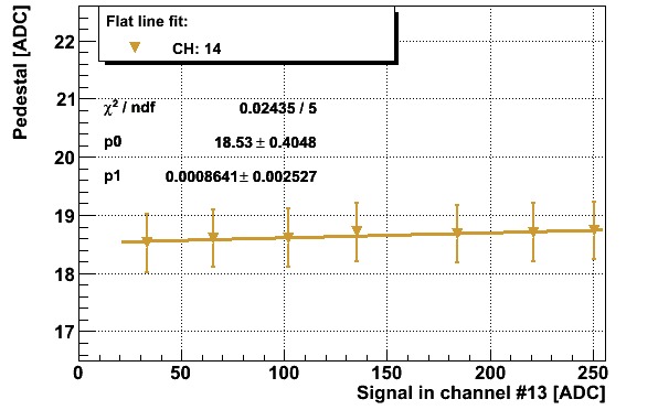
An example of the performed measurements is presented in Fig. 6. The measured pedestal is presented for all channels while in the channel the charge was injected with different amplitude values. In the neighboring lines the measured signal appears to remain well within one ADC unit.
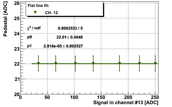
An attempt to estimate a possible variation is presented in Fig. 7, where for each channel a two-parameter linear fit is performed in the analyzed input signal range, confirming a negligible charge leakage between the channels. A small trend is possibly visible in channel , which is processed by the same FPGA of the channel , where the signal was injected. Conservately, for each data point the uncertainty was taken as being half of the ADC bin size. This assumption is motivated by the narrow pedestal distribution, which is typically well within one ADC unit.
7 Dynamic Range and Linearity of the Readout Electronics
During data taking the dynamic range of the ADC should linearly cover the entire possible energy range deposited by the impinging neutrons. In the Anger Camera the scintillating light is initially generated during the drift of the generated electron cloud in the gas volume and then in the amplification stage of the micro-strip. At the exit window of the camera the light is collected by a set of vacuum photomultipliers (four PMTs in the prototype used at FZJ), and converted in a current signal. The amplitude of the signal depends eventually on several factors as the tension applied to the micros-trip, to the drift field, and to the photomultipliers, and the amplifying stage of the JUDIDT electronics, which is set to ten for this type of experiment. The electronics gain can be eventually changed in order to cover the dynamic range allowed by the investigated physics process. This can be achieved by using a proper capacitor in the main amplification stage.
Special care should be taken to the preamplifier configuration to fit the characteristic of both the incoming signal from the PMTs and of the JUDIDT amplifying stage. An input signal of mV can already saturate the amplifier, when the device is configured for a gain of factor ten, (as verified directly on the board by a scope).
The linearity of the system response was tested with the laboratory data acquisition system and using a negative tailed pulse at different amplitude values. The minimum injected voltage was the reference point of the measurement, and was extracted at the oscilloscope after maximally attenuating the signal with the Tennelec device. This device offers several combinations of attenuating values by properly activating the several switches available in the device. By de-selecting those switches a larger amplitude could be injected in the readout electronics without modifying the setting of the pulse generator.
An example of this measurement is presented in the upper panel of Fig. 8 for tailed pulses with s decaying time.
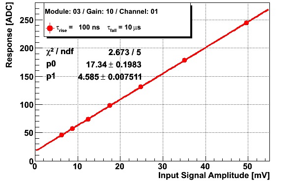
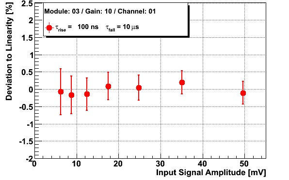
A linear fit to the experimental data is performed; for each measurement setup a Gaussian distribution is generated, and the uncertainty on the mean value is calculated, following [7], as . The residuals to the linearity are calculated dividing the deviation of the measured experimental points from the linear fit results over the fit values. The results are presented as percent in the bottom panel of Fig. 8, showing a linearity well stable within within the statistical uncertainty of the measurement.
It should be noted that by using an analogue pulse generator the minimum injected voltage (our reference) could not be measured with enough precision. This could possibly affects the extraction of the fit slope, but not any conclusion about the linearity of the system, being the larger input voltage points determined by rescaling the measured reference point using the switches of the Tennelec device.
The system appears therefore reasonably linear, while keeping the input signal below the saturation region of the main amplifying stage, above mentioned. The gain of factor of the electronics was verified directly on the board before the ADC stage via a high-impedance scope.
8 Gain of the Readout Electronics and ADC Calibration
Although great care is taken in the design a construction of each independent channel to have the same signal processing, eventually slight differences in the gain are observed, as shown in Tab. 1. Here, a signal of mV was injected separately in each channel of two modules with nominal gain , and the corresponding amplified and shaped signal was measured at the end of the amplifying stage before the ADC module, using a high-impedance (1 MOhm) probe. In the module Nr.03 (Nr.04) a drop in the gain up to () can be observed with respect to the maximum value, and a maximum deviation with respect to the nominal value up to (); thus verifying that indeed a non-homogeneous gain among channels and boards as well is present.
| Module 03 | ||||||||
|---|---|---|---|---|---|---|---|---|
| Channel: | 00 | 01 | 02 | 03 | 04 | 05 | 06 | 07 |
| Signal [mV]: | 390 | 395 | 400 | 390 | 405 | 400 | 395 | 395 |
| Gain: | 9.7 | 9.9 | 10.0 | 9.7 | 10.1 | 10.0 | 9.9 | 9.9 |
| Channel: | 08 | 09 | 10 | 11 | 12 | 13 | 14 | 15 |
| Signal [mV]: | 400 | 400 | 395 | 410 | 405 | 400 | 390 | 390 |
| Gain: | 10.0 | 10.0 | 9.9 | 10.2 | 10.1 | 10.0 | 9.7 | 9.7 |
| Module 04 | ||||||||
| Channel: | 00 | 01 | 02 | 03 | 04 | 05 | 06 | 07 |
| Signal [mV]: | 390 | 360 | 360 | 370 | 370 | 370 | 370 | 370 |
| Gain: | 9.7 | 9.0 | 9.0 | 9.2 | 9.2 | 9.2 | 9.2 | 9.2 |
| Channel: | 08 | 09 | 10 | 11 | 12 | 13 | 14 | 15 |
| Signal [mV]: | 360 | 370 | 370 | 360 | 370 | 365 | 375 | 360 |
| Gain: | 9.0 | 9.2 | 9.2 | 9.0 | 9.2 | 9.1 | 9.4 | 9.0 |
This feature can be easily cured by properly adjusting the high voltage of the involved photo-multipliers, after a gain matching procedure, as for example, described in Sec. 10.
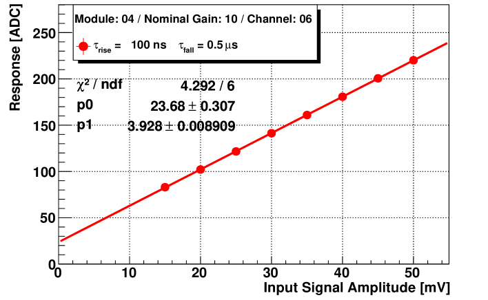
From simple considerations in Sec. 2 an estimation for the signal resolution was obtained as mV per measured ADC for a board with ideally a gain of . As we have proved, this is not the case, because the gain can vary largely between channels and boards. Therefore it is interesting to measure the signal resolution directly in the test bench facility. Using the digital pulse generator BNC/PB-5 the resolution was directly measured injecting pulses with increasing and well known amplitude. An example of this analysis is presented in Fig. 9.
Performing a linear fit to the experimental data, from the inverse of the extracted slope the overall system ADC resolution of mV / ADC can be obtained for the analyzed channel. This measurement confirms again the high linearity of the readout system.
9 Rate Efficiency
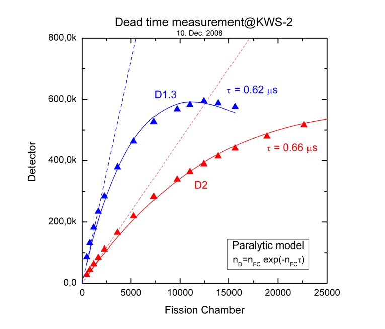
The DAQ system is forseen to cope with high rate fluxes of some hundreds of kilohertz, and has been therefore tested to fullfil this requirement. An interesting measurement was in the past done in the experimental hall at the KWS-2 detector in FRM-II. Taking as reference the counting of a fission chamber, the detector KWS-2, using the JUDIDT electronics, was located at two different locations with respect to the flux exit window. The result of this measurement is presented in Fig. 10.
At FZJ a similar measurement has been performed using a tail pulse generator operated at different frequency values, and storing the data with the timestamp granularity of one millisecond, Fig. 11.
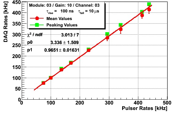
It is clear that following this technique no statistical Poisson fluctuation in the flux can be observed, as instead is expected in a reactor beam. The efficiency is calculated for each run, and its mean is evaluated considering several runs. The displayed uncertainty is obtained considering the maximum deviation between all considered runs. The points at large rate values show larger uncertainty, which can be temptatively understood as given by the not sufficiently small timestamp granularity. Superimposed to the points is shown a linear fit, whose slope appears to be driven downwards by the high rate points, possibly due to the fact that the multi-purpose DAQ developed in the laboratory is not yet optimized for this specific measurement. The peaking rate values, superimposed in the plots, are typically larger than the mean efficiency values, thus supporting this scenario.
It is additional interesting to investigate also how homogeneous is the data accumulation rate of the electronics with respect to the amplitude of the incoming signal. This feature was studied by injecting a tailed signal with varying amplitude and fixed pulse rate while measuring the rates with the laboratory DAQ system. No precise amplitude value could be determined directly by the front panel of the analogue BNC generator; nevertheless this uncertainty should not have an effect on this analysis. An example of this measurement is presented in Fig. 12
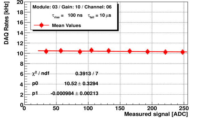
For each injected signal configuration the DAQ rate is calculated consecutively each accumulated events, and the ADC mean of the several measurements is shown for each signal amplitude. The presented uncertainty is only systematics, and represents conservately half of the maximal deviation of the observed rate values (deviations due to the load of computing time of the laboratory DAQ when performing internal routines such as, among the others, listening at clients or dumping the running configurations). A two-parameter linear fit is performed to the experimental data showing no anomalous trend in the acquisition rate.
10 Gain Matching of the Photomultipliers
In order to correct for the above mentioned gain mismatch among the different readout channels in the system, comprising the photomultipliers and the amplifying electronics, a blue light LED system has been implemented to equalize the response of all PMTs. The results presented in this paper were obtained using the Hamamatsu vacuum photmultipliers R580 which have a nominal photo-cathode diameter of mm.
The LED is centrally located in a hole in the front-head structure, where the PMT photocathodes (symmetrically located with respect to the LED) watch at the exit window of the Anger Camera (where the scintillating light is generated). Blue light is emitted by energizing the LED with a positive voltage pulse with a width and amplitude of approximately ns and V. The emitted light does not reach directly the photocathodes, but can reach them only upon isotropic backward reflexion on the chamber window, thus allowing for a reasonably uniform illumination of the photomultiplier photocathodes.
When properly tuning the high voltage value of the individual PMTs, the corresponding signal distributions can be acquired with similar mean values and width (RMS), recovering any possible initial gain mismatch of the different channels of the system. An example of this procedure, after proper baseline correction performed as described above, is presented in Fig. 13, using a positive pulse with amplitude V.
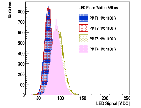
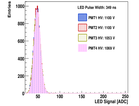
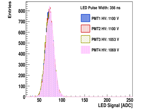
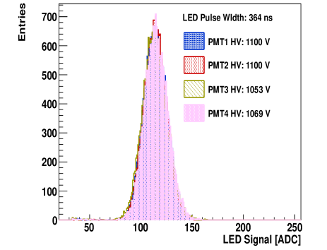
While properly tuning the high voltage of the photomultipliers a gain matching among the channels can be obtained. The stability of the procedure against unexpected effects is clearly visible by modifying the width of the pulse to the LED, and observing a stable gain matching. It should be also mentioned that this procedure to gain-match the readout channel should be, in principle, re-done whenever the system is modified (e.g. after the replacement of a photomultiplier, of a voltage divider, after the change of the pre-amplifier configuration, and so on).
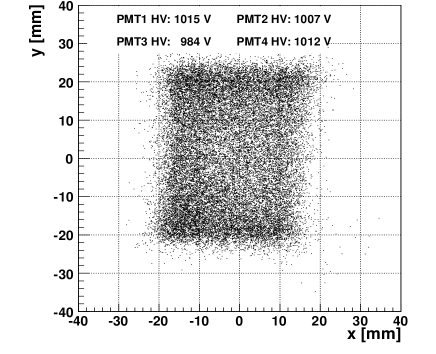
The 2D distribution of the reconstructed and coordinates for the LED-generated photons is presented in Fig. 14 confirming (qualitatively) the goodness of the presented gain matching procedure.
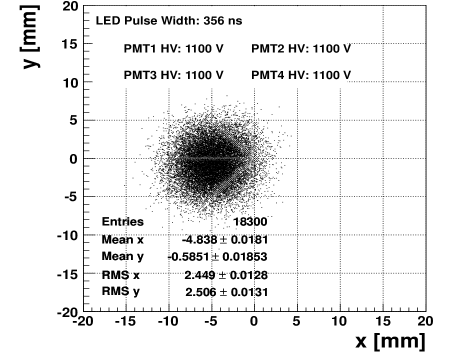
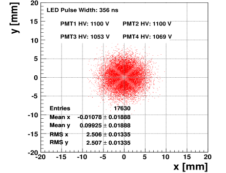
The coordinates here presented were obtained using the "center of gravity" method (COG) developed following this procedure: A left-right and top-down signal asymmetry is calculated from the response of each photomultiplier:
| (1) |
Out of the signal asymmetries the coordinates are then calculated as [9]
| (2) |
mm being the side width of the virtual square enclosing the four photomultipliers. The photomultipliers PMT1 to PMT4 are located anticlock-wise starting from the top-right corner of the holding frame. More sophisticated methods are available in the literature [10, 11].
It is interesting to stress that this LED system could be used (with a slight modification of the DAQ software) to automatically monitor online any gain change (both long and short-term) providing the user a way to promptly act to correct for the observed gain mismatch and avoiding a bias of the measurement.
The pre-amplifier was configured to provide a small and Gaussian signal distribution from the LED in the readout while, at the same time, to keep the signal distribution from neutrons well within the ADC dynamic range when running the detector amplification stages at its nominal values. The decaying time of the output signal in the configuration used in our laboratory is s, being pF and kOhm. When needed, the LED distribution can be moved at larger ADC values by modifying the width and amplitude of the voltage pulse energizing the LED, as discussed in Fig. 13.
11 Towards Real Data Taking Conditions
Dedicated test-beam campaigns were done by the collaboration to investigate the performance of the Anger Camera prototype in combination with the JUDIDT readout system. The results, obtained after a detailed detector calibration and offline analysis, are shown in a dedicated report [5]. Here we will present, for example purpose, how the Camera runs in presence of real neutron, using the neutron source.
The camera, assembled colleagues of the Technische Universität München, is filled by a + gas mixture at the pressure of and bar, respectively. The back-side view is presented in the left panel of Fig. 15.
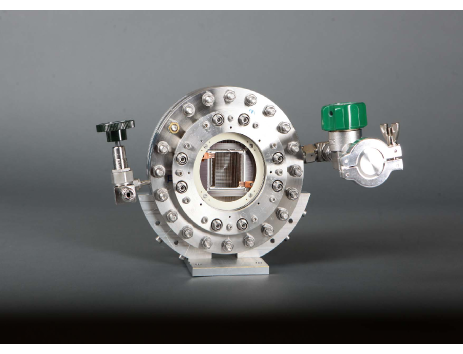
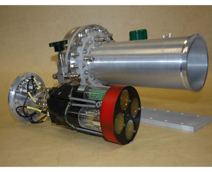
Visible is the hosted micro-strip plate with an active are of x mm2, located before the exit window for the scintillating light. The aluminum case, shown in the right panel of the picture, was designed and assembled at ZEA-2. It is quite flexible, allowing for hosting different types of PMTs.
The drawback of this flexible configuration is that the coverage of the amplifying micro-strip by any of the four photomultipliers can be different according to the orientation of the mask supporting the PMTs in the aluminum case, thus possibly biasing the measurement of the neutron impinging point. It is clear that in case of a running experiment a fest structure will be used to host the PMTs, such to cover uniformly the active area of the micro-strip which is responsible eventually of the largest amount of the scintillation process.
An example of the signal deposited in the chamber by neutrons via scintillating light is shown in the left panel of Fig. 16.
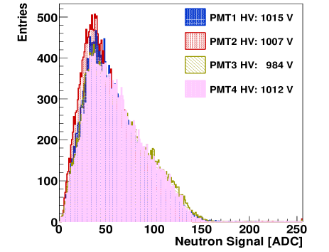
In the laboratory the PMT mask was oriented visually to have a grid of 2x2 light collectors. The detector was located at approximately cm from a -symmetrically radiating neutron source. Possibly due to the above mentioned reason, a small residual signal asymmetry is still visible in one channel, as shown in the left panel of Fig. 16 (PMT2, which is located in the bottom right corner along the neutron flux direction). Although the not perfect configuration of the PMT mask, the reconstruction of the neutron impinging points reproduces quite well the shape of the micro-strip (x mm2), shown in the right panel of the picture. Here the coordinate frame was used with respect to the neutron flux. Note that also the small-degree tilt of the plate, which is due to mounting reasons, is reproduced in the analysis.
12 Conclusions
During the year 2012 deep systematic studies have been performed to characterize the readout electronics JUDIDT developed at Forschungszentrum Jülich, designed for instruments for neutron detection, in particular as a readout system for an Anger Camera prototype filled with - gas mixture.
The more significant results are presented and described in this paper, showing that the overall performance of the electronics was found to be excellent, with an overall signal resolution typically around mV per ADC. The intrinsic electronic noise was investigated, and was found to be within fractions of millivolt. The charge leakage between neighboring channels is within one ADC channel.
Comparing the input channels of a single board, the pedestals showed a variable spread, which can be corrected for, using the flexible way of the system to cover a specific dynamic range by steering via software the baseline, individually for each channel, thus providing a similar dynamic range for all channels.
Several measurements, including the ADC calibration, confirmed a linear response of the system in all the allowed dynamic ADC range.
When used as readout system for the Anger Camera optimal spatial resolution below one mm for the neutron impact points was obtained, and a reasonable dead time measured up to kHz [5].
All these measurements have basically fulfilled the requirements to operate the electronics in a neutron beam environment, and the features which could be fixed in the next version of the DAQ software (as the automation of some monitoring and calibration procedures).
At the end of 2013, the Anger Camera detector with the JUDIDT readout system is proposed to be used on a regular neutron instrument in the FRM-II experimental hall, for further evaluation and real scientific experiments. Having the detector operational on a real instrument is the ultimate test to convince potential users of its performance and reliability. We expect that several scientists will be willing to equip their instrument with a copy of this detector.
Acknowledgments
The authors gratefully acknowledge R. Foester, T. Kollmann, C. Wesolek, and the colleagues of the ZEA-2 Workshop for their valuable technical contribution to the results here presented. We are also deeply grateful to the ZEA-2 Management for its significant efforts in supporting this project.
References
-
[1]
W. Gläaser and W. Petry,
’The new neutron source FRM-II’,
Physica B, vol. 276-278, (2000) 30. -
[2]
R. Wagner, W. Bräautigam, D. Filges,
and H. Ullmaier,
The project ’European Spallation Neutron Source (ESS)’: Status of R&D Programme,
Physica B, vol. 276-278, (2000) 38. -
[3]
G. Kemmerling et al.,
A New Two-Dimensional Scintillation Detector System for Small-Angle Neutron Scattering Experiments,
IEEE TRANSACTIONS ON NUCLEAR SCIENCE, VOL. 48, (2001) NO.4. -
[4]
FP7/NMI3,
Integrated Infrastructure Initiative for Neutron Scattering and Muon Spectroscopy (NMI3). Project funded by the th Framework Programme (FP7).
http://nmi3.eu. -
[5]
K. Zeitelhack et al.,
An Anger Camera prototype for Neutron Detection,
in preparation. -
[6]
R. Fabbri,
A Data Acquisition and Monitoring System for the Detector Development Group at FZJ/ZEA-2,
arXiv:1304.2894v1, FZJ-2013-01939. -
[7]
K. Nakamura et al.,
Review of Particle Physics,
Journal of Physics G 37, 075021 (2010). -
[8]
G. F. Knoll,
Radiation Detection and Measurement,
John and Wiley & Sons, Inc. -
[9]
F. Piscitelli,
PhD Thesis, University of Roma 2 Tor Vergata 2010,
A Study on a Thermal Neutrons Detector Prototype. -
[10]
A. Morozov,
ANTS - a Simulation Package for Secondary Scintillation Anger-Camera Type Detector in Thermal Neutron Imaging,
JINST 7 P08010. -
[11]
M. Beckmann et al.,
The Longitudinal Polarimeter at HERA,
NIM A 479 (2002) 334.