Asymmetric scattering of Dirac electrons and holes in graphene
The relativistic nature of Dirac electrons and holes in graphene profoundly affects the way they interact with impurities imp_gr1 ; imp_gr2 ; mc_2 ; mc_3 ; mc_4 ; kotov ; rossi . Signatures of the relativistic behavior have been observed recently in scanning tunneling measurements on individual impurities crommie_2 , but the conductance measurements in this regime are typically dominated by electron and hole puddles martin ; mc_3 ; mc_4 . Here we present measurements of quantum interference noise and magnetoresistance in graphene pn junctions. Unlike the conductance, the quantum interference noise can provide access to the scattering at the Dirac point: it is sensitive to the motion of a single impurity ucf_2 ; rossi ; berezovsky , it depends strongly on the fundamental symmetries that describe the system lee_1 ; bla_1 and it is determined by the phase-coherent phenomena which are not necessarily obscured by the puddles rahman . The temperature and the carrier density dependence of resistance fluctuations and magnetoresistance in graphene p-n junctions at low temperatures suggest that the noise is dominated by the quantum interference due to scattering on impurities and that the noise minimum could be used to determine the point where the average carrier density is zero. At larger carrier densities, the amplitude of the noise depends strongly on the sign of the impurity charge, reflecting the fact that the electrons and the holes are scattered by the impurity potential in an asymmetric manner.
Conductance fluctuations in disordered electron systems are a consequence of the quantum interference between the trajectories of charge carriers scattered on impurities lee_1 ; bla_1 . In the case of static disorder within a phase coherent volume, the conductance shows reproducible aperiodic fluctuations, known as universal conductance fluctuations (UCF), as a function of magnetic field or chemical potential lee_1 . If the impurity configuration changes slowly over time, the trajectories of the scattered electrons will also change. This causes the conductance to fluctuate in time, and the noise power shows a 1/f type dependence ucf_2 ; ucf_4 ; ucf_5 . One can easily distinguish this mechanism from other sources of 1/f noise by its temperature dependence. While the conventional noise will typically increase with increasing temperature, the quantum interference noise will do the opposite: even though the impurities may fluctuate less at lower temperatures, the phase coherent volume increases, including more impurities and increasing the contribution to the noise.
The effects of quantum interference also lead to corrections to the average conductance: interference between backscattered paths causes weak localization in disordered electronic systems with weak spin-orbit coupling berg_1 . In graphene, the conservation of pseudospin prevents backscattering on long-range disorder potentials, and localization is expected only due to scattering on atomically sharp, short-range disorder, which can couple the two valleys mc_4 . Quantum corrections and UCF as a function of magnetic field and chemical potential in graphene have been studied both experimentally and theoretically mc_4 .
In the vicinity of the Dirac point, however, the predictions of the quantum transport theory do not strictly hold and analytical treatment is not always possible. In clean graphene, transport in this regime is expected to be pseudodiffusive, occurring through quantum tunneling of evanescent modes tworzydlo . In the presence of disorder, however, the transport is dominated by the electron and hole puddles martin ; rr_1 . It has also been argued that charged impurities dominate the conductivity in graphene and that the minimum conductivity is not determined by the vanishing carrier density, but rather the added carrier density which neutralizes the impurity potential mc_3 ; adam .
In this work, we show that the time-dependent resistance fluctuations are determined by a different mechanism than the resistance itself, and that they are due to fluctuations of the electron trajectories that take part in quantum interference. We argue that these measurements can access the details of impurity scattering in the vicinity of the Dirac point and that the asymmetry in the noise as a function of gate voltage is related to the asymmetry in the scattering of relativistic electrons and holes by the impurities present in the system.
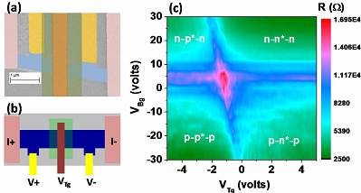
The devices were fabricated by mechanical exfoliation of natural graphite (see supporting materials for the details of the sample fabrication). Scanning electron microscope image of a typical device is shown in Fig. 1(a). All the measurements were done in a 4-probe geometry (schematic shown in Fig. 1(b)) to minimize the effects of contacts. In Fig. 1(c) we show the resistance (measured at 250 mK) as a function of both back gate () and top gate voltage () for a p-n-p transistor device (SL1). All four regions (marked by p-p∗-p, p-n∗-p, n-n∗-n and n-p∗-n) are clearly visible ( denotes the carrier type under the top gate). In the absence of top gate voltage, the charge neutrality point () was found at volts.
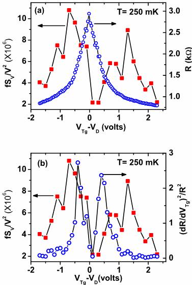
Low-frequency noise measurements were carried out using the ac noise measurement technique scofield (see supporting materials for the details of the noise measurement). Both invasive and external voltage probes external_1 were used for the noise measurements. The power spectral density () shows dependence at all top gate voltages with values of close to 1 (see supporting materials, Fig. S1). Normalized noise power density ( or ) was found to be independent of the bias current or voltage, ruling out any effects of heating by the bias current. The normalized noise power () shows a non-monotonic behavior as a function of top gate voltage. In Fig. 2(a) we show both the resistance and normalized noise as a function of . It is important to note that the peak in the resistance and the minimum in the noise () do not coincide (see supporting materials, Fig. S2). To ascertain that this is not due to the experimental delay between the two measurements, we carried out simultaneous measurements of both noise and resistance as a function of (see supporting materials Fig. S2). In several samples, the noise power () itself showed the non-monotonic behavior as a function of gate voltage (see supporting materials, Fig. S3 and S4). The noise measurements were highly reproducible over time at all temperatures, and did not depend on the direction or scan step of the gate voltage (see supporting material, Fig. S3 and Fig. S4).
Measurements of 1/f noise in graphene have been reported before m1 ; m2 ; m3 ; m4 ; m5 . The non-monotonic behavior as a function of gate voltage has been attributed to charge noise m1 , interplay between majority and minority carriers m2 and competition between long-range and short-range scattering m3 ; m5 . We note that the noise observed here is markedly different from that discussed above - in our samples, the noise amplitude increases with decreasing temperature, in contrast to the previously reported results (see supporting material, Fig. S5). Non-monotonic 1/f noise has also been recently predicted due to non-universal conductance fluctuations in a crossover between a pseudodiffusive and symplectic regime in clean graphene rossi .
In order to explain the origin of the noise, we consider three possible contributions: carrier density fluctuations, impurity fluctuations and contributions from the pn junction interfaces.
If we assume that the noise is determined entirely by the fluctuations in the carrier density number_1 or mobility mob_1 , then the normalized noise power, and the contribution to the resistance fluctuations due to the carrier density should closely follow each other and exhibit a minimum at the same value of the gate voltage m5 ; m1 . However, the two do not coincide, as shown in Fig. 2(b), indicating that the noise is not dominated by the fluctuations in the carrier density.
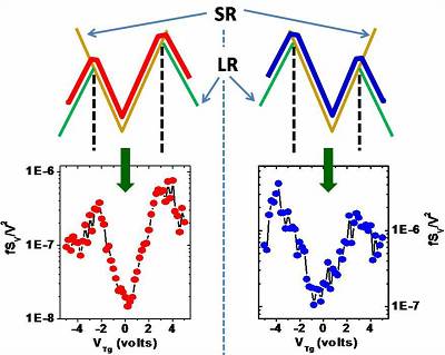
Two main types of impurities are known to play a crucial role in determining the electronic transport properties of graphene: short-range (SR) and long- range (LR) impurities mc_2 ; mc_3 ; mc_4 . SR impurities contribute to the resistance in a density-independent manner ando_1 , while the effect of LR impurities is inversely proportional to the density ando_2 . Consequently, if scattering on SR impurities were the dominant source of resistance fluctuations, then the normalized noise would be expected to increase monotonically with increasing carrier concentration (). On the other hand, if LR impurities dominated the noise, then its magnitude would decrease with increasing . A cross-over from SR to LR impurity-dominated scattering could therefore account for the nonmonotonic behavior as a function of gate voltage.
A possible evidence of such a crossover can be found in the temperature dependence of resistance and magnetoresistance as a function of , shown in Fig. 3. In Fig. 3(a) we show dependence of resistance at two different temperatures for a typical device (SL3). It is clear that the resistance increases with decreasing temperature in the vicinity of the Dirac point, but does not otherwise show a strong temperature dependence. Normalized noise and the temperature-dependent part of resistance are shown together as a function of top gate voltage in Fig. 3(b). It is interesting to note that the regime in which the noise increases as a function of gate voltage coincides with the range of gate voltages for which the resistance depends on temperature (shaded region in Fig. 3(b)). Outside the shaded region, the resistance becomes nearly temperature independent and the noise starts to decrease as a function of on both sides.
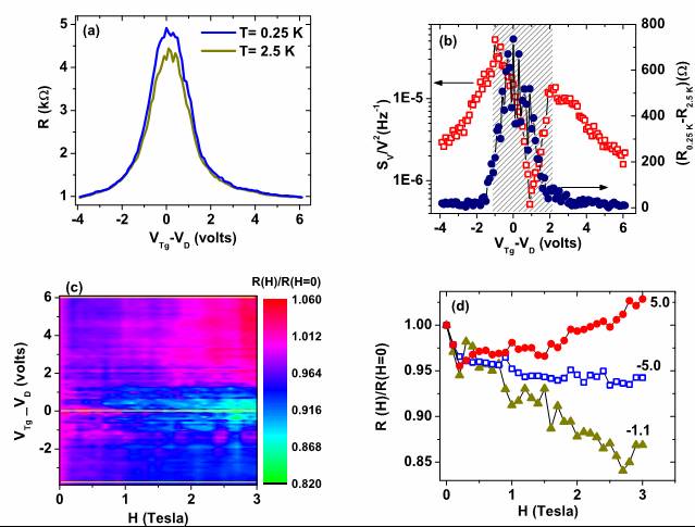
The increasing resistance with decreasing temperature suggests localization, which should then also be apparent in magnetoresistance measurements. In Fig. 3(c) and 3(d) we show the magnetoresistance as a function of for the same sample. The magnetoresistance is negative and relatively large near the charge neutrality point (CNP).
The negative magnetoresistance might be expected as a result of weak localization CG1 and would suggest the important role of short range scatterers mc_4 . Negative magnetoresistance over relatively large magnetic field has also been observed in chemically modified graphene where short range scatterers were known to be present fl_gr_1 ; hi_gr_1 .
We find that the sign and the magnitude of the magnetoresistance depends on the position of the CNP as a function of gate voltage. In particular, if the CNP is located at negative gate voltage, then we observe negative MR up to relatively large negative gate voltages. It is evident in Fig. 3(c) and (d) that the maximum negative MR is observed at the CNP (located at = -1.1 volts at zero back gate voltage). Away from the CNP, the resistance shows an upturn as a function of magnetic field on the electron side (positive gate voltage) at a low gate voltage. On the hole side (negative gate voltage), negative MR is observed up to large negative gate voltages, though the magnitude decreases with the increasing gate voltage. Similarly, if the CNP is located at the positive gate voltage, larger magnetoresistance is observed on the electron side. Such asymmetric effect of backscattering is consistent with a recent STM observation of quasiparticle interference on localized scattering centers crommie_1 . The quasiparticle interference implies backscattering and was observed on scattering centers only in the electron puddles in the sample in which the CNP was located at positive gate voltage crommie_1 .
We also find that the position of the CNP affects the noise amplitude away from the CNP. Specifically, as we move away from the minimum, the noise as a function of gate voltage becomes asymmetric with respect to the gate voltage, showing two peaks of different heights. We found that the peak height and position are related to the position of the CNP: if the CNP is located in the negative side of the gate voltage then the peak in the hole side is larger (Fig. 2(a), 3(b), and 5(b)). Similarly, if the CNP is located at a positive value of the gate voltage (electron side), than the noise peak is larger on the electron side(Fig. 4(d)). We note that an asymmetric contribution to 1/f noise could arise due to fluctuating gate leakage current m5 . However, this contribution can be ruled out in our experiment (see supplementary information for details).
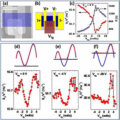
To rule out the possibility that the measured noise is generated at the p-n junction interfaces (between two regions characterized by two different types of charge carriers), we fabricated a parallel p-n junction marcus_1 (shown in Fig. 4(a)) and studied the noise characteristics as a function of and . As the top gate voltage affects half of the sample in a parallel configuration (see Fig. 4(b) for a schematic), the resistance of the sample will be determined by the parallel combination of the resistance of the two segments (portions with and without top gate) and lowest resistive path will dominate. However, the noise of the entire system will be determined by the maximum noise in either of the two segments. In the absence of the top gate voltage, the minimum in the noise is found at volts (Fig. 4(c)). As a function of , two maxima appear in the noise (Fig. 4(d)). As the back gate is set at the value at which the noise shows a minimum, we can safely assume that the maxima in the noise arise from the part of the sample under the top gate. We found that the peak on the electron side is larger than the peak on the hole side in this case (Fig. 4(d)). Away from the CNP the noise increases with on both sides (Fig. 4(c)). As a result, the shape of the vs. characteristics changes continuously with changing (Fig. 4(e) and (f)). It is evident from the data that noise is always large when the carriers under the top gate are electrons. In Fig. 4(f) we see that for = 0 volts the carriers are holes ( = -26 volts). If we add more holes by applying a negative , we find that the noise increases slightly. On the other hand, for positive , the charge carriers under the top gate are electrons and a sharp increase in noise is observed. This excess noise on the electron side suggests that the scattering by the impurities present in the system has a stronger effect on electrons compared to holes.
The observed noise is clearly not due to the noise generated at the p-n junction interface, because then we would not observe it in case of a parallel p-n junction. This also implies that the electron and hole puddles that form near the CNP are not responsible for the observed noise. Specifically, if the noise is determined by the resistance fluctuations at the p-n junctions formed by the puddles, then we would expect the noise to decrease with increasing gate voltage away from the CNP. As we move away from the CNP by increasing the gate voltage, the typical size of one type of puddles will decrease, so the effective p-n junction area will also decrease. Consequently, any noise generated by the current floeing through a pn junction interface should decrease with increasing gate voltage, opposite to our observations close to CNP. In the random resistor model of puddles in graphene, the resistance is determined by the weak links between p and n type regions rr_1 . Any fluctuation of the junction resistance will give rise to low frequency noise. However, if the noise were generated due to the fluctuations of the p-n junction resistance, then we would not expect to see a strong temperature dependence, since the resistance in graphene does not vary strongly with temperature (see supporting materials Fig. S5).
We also found that the negative magnetoresistance persists up to relatively large value of negative gate voltage (hole-type carriers), when the CNP is located at the negative side of the gate voltage and vice versa. We note that magnetoresistance itself could possibly be due to the transmission through the pn interfaces formed by electron and hole puddles at low carrier densities, although it is not obvious that this mechanism would result in negative magnetoresistance falko .
It is evident that the resistance increases with decreasing temperature in the same range of gate voltages for which the noise increases as a function of gate voltage (shaded region in Fig. 3.b). The maximal change in the resistance does not coincide with the minimum in the noise, which suggests that the resistance and the noise are dominated by different phenomena. This is also the same regime in which we see the largest negative magnetoresistance. All three phenomena (increasing resistance with decreasing temperature, increasing noise as a function of gate voltage and negative magnetoresistance) could be explained in terms of scattering on SR impurities. STM measurements support the relevance of SR scatterers near the Dirac point: the results on epitaxialy grown graphene found that SR scatterers are the dominant scattering centers rutter . A more recent STM experiment found scatterers of the SR type only in the electron puddles in samples in which the charge neutrality point was located on the electron-doped side crommie_1 , which is consistent with the asymmetry observed in our experiments.
Keeping this in mind, we can understand the asymmetric shape of the noise through a model shown in Fig. 5. For a positive value of CNP, the backscattering and the increase of noise is observed over a large positive gate voltage. Assuming that the SR scatterers dominate in this regime, we would expect the noise to increase with increasing carrier density. This also implies that it is actually the minimum in the noise, not the maximum in resistance, that reflects the vanishing carrier density. If we increase the gate voltage further, the noise becomes dominated by LR scatterers and we expect to see a decrease in the noise with increasing gate voltage. Taken together, these two effects result in a non-monotonic and asymmetric shape of the noise as a function of the gate voltage. Similar results are obtained in the case when the CNP is located at a negative value of the gate voltage: Fig. 5 shows the model and the corresponding data for CNP located at +8 volts (left panel) and -10 volts (right panel).
We note that a qualitatively similar non-monotonic behavior in the quantum interference noise was predicted recently due to a crossover from the pseudodiffusive to symplectic metal regime rossi . While this could easily describe our noise data, it is not obvious that our samples are in the relevant regime. More detailed theoretical treatment would be needed to show whether the temperature dependence and magnetoresistance observed in our experiments are also consistent with such a crossover.
Unlike conductivity, which is dominated by charge impurities mc_3 ; adam , we find that the quantum interference noise is dominated by scattering on disorder of a short-range type in the vicinity of the Dirac point. The observed asymmetry in the noise with respect to the gate voltage suggests that electrons and holes scatter differently from the disorder potential. The nature of this asymmetry is consistent with that observed in conductivity mc_3 and STM crommie_1 measurements, and can be related to the relativistic nature of electrons and holes in graphene. The minimum in the noise can be used to determine the gate voltage at which the carrier density vanishes, which, in disordered graphene, is not identical to the point at which the conductivity shows a minimum. This shows that quantum interference noise can be used as a probe that is complementary to conductivity and STM measurements and can be used to investigate the details of scattering of relativistic Dirac fermions.
References
- (1) Castro Neto, A. H., Guinea, F., Peres, N. M. R., Novoselov, K. S. & Geim, A. K. The electronic properties of graphene. Rev. Mod. Phys. 81, 109-162 (2009).
- (2) Chen, J. H., C. Jang, S. Adam, M. S. Fuhrer, E.D. Williams, and M. Ishigami, Charged Impurity Scattering in Graphene, Nature Phys. 4, 377 (2008).
- (3) Das Sarma, S. , Adam, S., Hwang, E. H. & Rossi, E. Electronic transport in two dimensional graphene. Rev. Mod. Phys. 83, 407 (2010).
- (4) Shytov, A. V., Katsnelson, M. I. & Levitov, L. S. Atomic collapse and Quasi-Rydberg states in graphene. Phys. Rev. Lett. 99, 246802 (2007).
- (5) Shytov, A. V., Katsnelson, M. I. & Levitov, L. S. Vacuum polarization and screening of supercritical impurities in graphene. Phys. Rev. Lett. 99, 236801 (2007).
- (6) V. N. Kotov, B. Uchoa, V. M. Pereira, F. Guinea and A. H. Castro-Neto, Electron-Electron Interactions in Graphene: Current Status and Perspectives. Rev. Mod. Phys. 84, 1067 (2012).
- (7) Rossi E., Bardarson J. H., Fuhrer M. S. & Das Sarma S., Universal conductance fluctuations in Dirac materials in the presence of long-range disorder. Phys. Rev. Lett. 109, 096801 (2012).
- (8) Wang Y., Brar V. W., Shytov A. V., Wu Q., Regan W., Tsai H.-Z., Zettl A., Levitov L. S. & Crommie M. F., Mapping Dirac quasiparticles near a single Coulomb impurity on graphene. Nat. Phys. 8, 653-657 (2012).
- (9) Martin J., et al. Observation of electron-hole puddles in graphene using a scanning single-electron transistor. Nature Physics 4, 144-148 (2008).
- (10) Feng, S., Lee, P.A. & Stone, A.D., Sensitivity of the Conductance of a Disordered Metal to the Motion of a Single Atom: Implications for 1/f Noise. Phys. Rev. Lett. 56, 1960-1963 (1986).
- (11) J. Berezovsky, M. F. Borunda, E. J. Heller and R. M. Westervelt, Imaging coherent transport in graphene (part I): mapping universal conductance fluctuations. Nanotechnology 21, 274013 (2010).
- (12) Lee P. A., Stone A. D., and Fukuyama H. Universal conductance fluctuations in metals: Effects of finite temperature, interactions, and magnetic field. Phys. Rev. B 35, 1039-1070 (1987).
- (13) Altshuler , B. L. , Fluctuations in the Extrinsic Conductivity of Disordered Conductors. JETP Lett. 41, 648-651 (1985).
- (14) Rahman A., Guikema J. W., Lee S. H. & Marković N., Transmission of phase information between electrons and holes in graphene. Phys. Rev. B 87, 081401(R)(2013).
- (15) Altshuler, B. L. & Spivak, B. Z., Change of random potential realization and conductivity of small size sample. JETP Lett. 42, 447 (1985).
- (16) Birge, N. O., Golding, B. & Haemmerle, W. H., Electron Quantum Interference and 1/f Noise in Bismuth. Phys. Rev. Lett. 62, 195 (1989).
- (17) Bergmann G. Weak Localization in Thin Films, a time-of-flight experiment with conduction electrons. Phys. Rep. 107, 1-58 (1984).
- (18) Tworzydlo J., Trauzettel B., Titov M., Rycerz A. & Beenakker C. W. J., Sub-Poissonian shot noise in graphene. Phys. Rev. Lett. 96, 246802 (2006).
- (19) Cheianov, V. V., Fal′ko, V. I., Altshuler, B. L. & Aleiner, I. L. , Random resistor network of minimal conductivity in graphene. Phys. Rev. Lett. 99, 176801 (2007).
- (20) Adam S., Hwang E. H., Galitski V. M. & Das Sarma S., Self-consistent theory for graphene transport. PNAS 104, 18392 (2007).
- (21) Scofield, J. H., ac method for measuring low frequency resistance fluctuation spectra. Rev. Sci. Instrum. 58, 985 (1987).
- (22) Huard, B., Stander, N. , Sulpizio, J. A. & Goldhaber-Gordon, D., Evidence of the role of contacts on the observed electron-hole asymmetry in graphene. Phys. Rev. B 78, 121402(R) (2008).
- (23) Heller, I., Chatoor, S., Männik, J., Zevenbergen, M. A. G., Jeroen B. Oostinga, J. B., Morpurgo, A. F., Cees Dekker, C. & Lemay, S. G., Charge Noise in Graphene Transistors. Nano Lett. 10, 1563-1567 (2010).
- (24) Xu, G., Torres, Jr., C. M., Zhang, Y., Liu, F., Song, E. B., Wang, M., Zhou, Materijal, Zeng, C. & Wang, K., Effect of Spatial Charge Inhomogeneity on 1/f Noise Behavior in Graphene. Nano Lett. 10, 3312-3317 (2010).
- (25) Zhang, Y., Mendez, E. E. & Du, X., Mobility-Dependent Low-Frequency Noise in Graphene Field-Effect Transistors, ACS Nano 5, 8124-8130 (2011).
- (26) Pal A. N., Ghatak S., Kochat V., Sneha E. S., Sampathkumar A., Raghavan S., & Ghosh A., Microscopic Mechanism of 1/f Noise in Graphene: Role of Energy Band Dispersion. ACS Nano 5, 2075-2081 (2011).
- (27) Kaverzin A. A., Mayorov A. S., Shytov A., & Horsell D. W., Impurities as a source of 1/f noise in graphene. Phys. Rev. B 85, 075435 (2012).
- (28) McWhorter A. L. in Semiconductor Surface Physics, edited by Kingston R. H. (University of Pennsylvania, Philadelphia)
- (29) Hooge F. N. 1/f noise is no surface effect. Phys. Lett. A 29, 139-140 (1969).
- (30) Shon N. H. & Ando T. Quantum Transport in Two-Dimensional Graphite System. J. Phys. Soc. Jpn. 67, 2421-2429 (1998).
- (31) Ando T. Screening Effect and Impurity Scattering in Monolayer Graphene. J. Phys. Soc. Jpn. 75, 074716 (2006).
- (32) Pollak M. & Ortuno M. Electron-Electron Interaction in Disordered Systems, edited by A. L. Efros and M. Pollak (North-Holland, Amsterdam, 1985).
- (33) Hong X., Cheng S.-H., Herding C., & Zhu J. Colossal negative magnetoresistance in dilute fluorinated graphene. Phys. Rev. B 83, 085410 (2011).
- (34) Matis B. R., Bulat F. A., Friedman A. L.,Houston B. H., & Baldwin J. W. Giant negative magnetoresistance and a transition from strong to weak localization in hydrogenated graphene. Phys. Rev. B 85, 195437 (2012).
- (35) Zhang, Y., Brar, V. W., Girit, C., Zettl, A. & Crommie, M. F., Origin of spatial charge inhomogeneity in graphene. Nat. Phys. 5, 722 (2009).
- (36) Williams J. R. & Marcus C. M., Snake States along Graphene p-n Junctions. Phys. Rev. Lett. 107, 046602 (2011).
- (37) Cheianov, V. V. & Fal′ko, Selective transmission of Dirac electrons and ballistic magnetoresistance of n-p junctions in graphene. Phys. Rev.B 74, 041403 (2006).
- (38) Rutter G. M., Crain J. N., Guisinger N. P., Li T., First P. N. & Stroscio J. A., Scattering and Interference in epitaxial graphene. Science 317, 219 (2007).