All-electrical spin injection and detection in the Co2FeSi/GaAs hybrid system in the local and non-local configuration
Abstract
We demonstrate the electrical injection and detection of spin-polarized electrons in the Co2FeSi/GaAs hybrid system using lateral transport structures. Spin valve signatures and characteristic Hanle curves are observed both in the non-local and the local configuration. The comparatively large magnitude of the local spin valve signal and the high signal-to-noise ratio are attributed to the large spin polarization at the Fermi energy of Co2FeSi in the well-ordered L21 phase.
Most spin-based semiconductor devices proposed to date rely on the ability to inject, transport, manipulate and detect spin-polarized carriers by purely electrical means.Datta and Das (1989); Sugahara and Tanaka (2004)As a fundamental proof of the all-electrical injection and detection of spins in a lateral device structure, non-local (NL) spin valve measurements with separated charge and spin currents are most appropriate.Johnson and Silsbee (1985); Jedema, Filip, and van Wees (2001) A spin accumulation generated in the transport channel is probed by a detector contact placed outside the current path. The detector measures an electrical signal that is purely spin related.
However, NL spin detection is not sufficient for operational spintronic devices that require an electrical signal in the local (L) configuration, i.e., an electrical spin signal resulting from a spin-polarized charge current flowing between a source and a drain contact. As a matter of fact, this kind of local spin valve operation is experimentally much more difficult to achieve than the NL one. The difficulty of the corresponding 2-point-arrangement is caused by the large electrical background signal and a strong contribution of the (not spin-related) contact resistances as well as parasitic effects.Tang et al. (2002) In order to minimize their influence, high spin injection and detection efficiencies are essential. Therefore a proper choice of the injector material can be crucial. From this point of view, half-metals are the ultimate solution regarding spin injection and detection, given that they are 100% spin polarized at the Fermi energy. The ferromagnetic Heusler alloy Co2FeSi is predicted to be a half-metal in its ordered L21 phaseWurmehl et al. (2005); Bruski et al. (2011) and is, in addition, closely lattice matched to GaAs.Hashimoto et al. (2005a) A promising spin injection efficiency of more than 50% has been demonstrated for Co2FeSi/(Al,Ga)As hybrid structures.Ramsteiner et al. (2008) In this Letter, we study the all-electrical injection and detection of spins in the non-local and local configuration in the Co2FeSi/GaAs hybrid system using a lateral device structure.
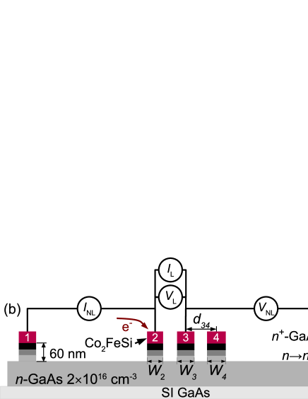
The investigated samples were grown by molecular beam epitaxy on semi-insulating (SI) GaAs(001) substrates, processed by wet chemical etching and photolithography, and finalized by the evaporation of Au bondpads. The samples consist of a 1500 nm thick, lightly -doped GaAs spin-transport layer ( cm-3) followed by a 15 nm thick transition layer and a 15 nm thick -layer ( cm-3). A 16 nm thick Co2FeSi layer was deposited onto this semiconductor structure at a substrate temperature of 280∘C. The highly -doped GaAs layer directly beneath the Co2FeSi forms a narrow Schottky barrier. Detailed information on the growth of the Heusler alloy Co2FeSi is provided elsewhere.Hashimoto et al. (2005a, b, 2007)
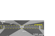
A scanning electron micrograph of the lateral device structure is shown in Fig. 1(a). The conductive mesa region is 400m2 large with stripe widths , , and of 9, 10, and 11m, respectively. The edge-to-edge spacing between stripes 2 to 4 is 3m leading to center-to-center separations of , , and m. The distances m are much larger than the spin diffusion length. The measurements in the L and NL configuration were carried out on the same samples by a conventional dc method with a current of 400 A as indicated in Fig. 1(b).
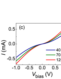
To evaluate the electrical properties of the Co2FeSi/GaAs Schottky contacts, we measured the two-terminal current (I)–voltage (V) characteristics for different contact pairs at different temperatures. The representative I–V characteristics measured between contacts 1 and 2 are shown in Fig. 1(c). The curves are nonlinear at all temperatures and show a very weak temperature dependence, indicating that tunneling through the interface is dominant.Kasahara et al. (2012) An insulator-like temperature behavior of the zero bias resistance (not shown here) supports this assumption.Jönsson-Åkerman et al. (2000)
Evidence for electrical spin injection and detection has been obtained by spin valve measurements. For these experiments, an external magnetic field () is applied parallel to the long side of the Co2FeSi stripes, i.e., along the easy axis of magnetization. The measured voltage depends on the relative magnetization orientation of the injector and detector stripes. During a sweep of the external field , this relative magnetization orientation changes twice from the parallel to the antiparallel condition due to slightly different coercive fields of the injector and detector caused by small variations in their stripe widths.
In the case of the NL measurements, spin-polarized electrons are injected into the GaAs channel at stripe 2 and drift towards stripe 1. The injected spins, however, diffuse in either direction from stripe 2. While there is no charge flow between stripes 3 and 5, the diffusion-induced imbalance in the population of the two spin channels leads to a chemical potential difference. Consequently, a NL voltage can be detected between stripes 3 and 5 as a measure of the spin-injection efficiency at stripe 2 [cf. Fig. 1(b)].
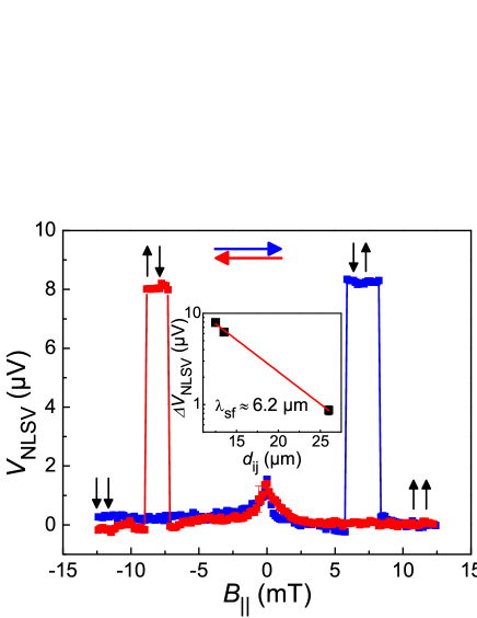
Fig. 2 shows the NL voltage measured in this way. The observed jumps in the voltage correspond to the switching between parallel and antiparallel magnetization of stripes 2 and 3. These characteristic spin valve signatures provide clear evidence for successful electrical injection and detection of spin polarized electrons.
At a distance from the injector, the voltage can be expressed by:Johnson (1993); Jedema et al. (2003); Fabian et al. (2007)
| (1) |
where is the bias current. , and are the resistivity, spin diffusion length, and the cross-sectional area of the nonmagnetic channel, respectively. is the efficiency of the spin injection (detection) at the respective contact. The () sign corresponds to the parallel (antiparallel) configuration of the injector and detector electrodes. From the dependence of the difference between the parallel and antiparallel signal on the injector-detector separation (cf. inset of Fig. 2) we estimate the spin diffusion length in the GaAs-channel as m. This value is in good agreement with values obtained by other groups for a similar doping of the GaAs channel.Lou et al. (2007); Ciorga et al. (2009); Salis et al. (2010)
The most robust proof for all-electrical spin injection and detection utilizes the Hanle effect, which reveals spin precession in an external magnetic field. For the corresponding experiments, the voltage is measured in the same way as described above. The in-plane magnetization orientations of the injector and detector stripes are kept fixed in the parallel or antiparallel configuration and the external magnetic field is now applied perpendicular to the sample plane. does not influence the in-plane Co2FeSi magnetization but causes a precession of the spins, which are injected into the GaAs channel. For parallel injector and detector magnetizations, the minimum voltage occurs at as confirmed by the measured data shown in Fig. 3. For finite fields , the spin precession leads to a misorientation of the spin polarization beneath the detector stripe diminishing the measured signal. The voltage in the Hanle geometry for the parallel configuration can be expressed by a one-dimensional spin drift-diffusion equation, which takes into account spin relaxation and precession, and whose solution reads:Jedema et al. (2002); Johnson and Silsbee (1985)
| (2) |
with .
is the spin diffusion coefficient, the spin relaxation time and
the Larmor frequency, where the electron g factor for GaAs is , is the Bohr magneton and is the reduced Planck constant.
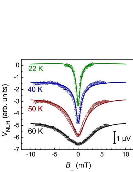
The NL Hanle signal vs. is displayed in Fig. 3 for different sample temperatures. The good agreement between the measured data and the fit (cf. Fig. 3) obtained by Eq. (2) using , , and as fit parameters provides further evidence for successful all-electrical injection and detection of spin polarized electrons. An increase in the temperature leads to an increase in the linewidth and therefore, as expected, to a decrease in the spin lifetime from 64 ns at 22 K to 11 ns at 60 K. Both of these values are comparatively large.Lou et al. (2007); Ciorga et al. (2009) Furthermore, using m, A, m (measured separately on the same sample using a Hall structure) and m2, a spin injection efficiency of has been extracted by the fitting procedure. Regarding our crude assumption , the obtained value of is in reasonable agreement with previous results obtained from Co2FeSi/(Al,Ga)As spin light-emitting diodes.Ramsteiner et al. (2008)
In the case of the local measurements, the spin and charge currents are no longer separated. The measure of the spin signal in the local configuration is the magnetoresistance (MR) ratio , where represents the resistance between stripes 2 and 3 [cf. Fig. 1(b)] for the parallel (antiparallel) source and drain contact magnetizations. The requirements for a sizable spin signal in the local configuration have been theoretically discussed.Fert and Jaffrès (2001); Dery, Cywiński, and Sham (2006); Fert et al. (2007) The most crucial parameter is the ratio of and . is the contact tunnel resistance at the interface between the ferromagnet and the semiconductor and the spin resistance is the product of the resistivity and the spin diffusion length within the semiconductor. A high ratio is needed to overcome the so-called conductivity mismatchSchmidt et al. (2000), but a too high value causes the spins to relax such that it prevents their detection. As a result, a window exists for the ratio for which the obtained signal is optimal.Fert and Jaffrès (2001); Fert et al. (2007) This window is given by:
| (3) |
where is the width of the contacts and and are the length and width of the channel, respectively. Due to the difficulty to fullfil these requirements, spin detection in the local configuration has been demonstrated in rare cases only.Ando et al. (2010); Ciorga et al. (2011); Nakane et al. (2010); Sasaki et al. (2011); Althammer et al. (2012); Kasahara et al. (2012)
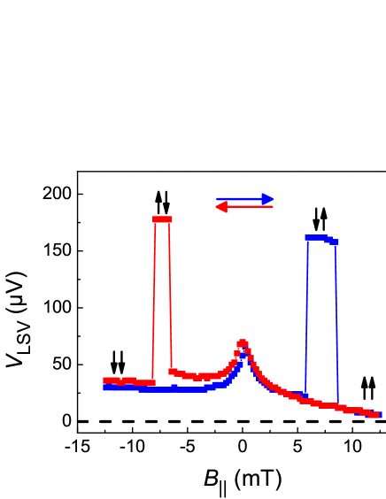
Local spin valve (LSV) measurements have been performed in the same manner as described above for the non-local case except for the change in the contact configuration. Here, a charge current () flows between contacts 2 and 3 and the spin valve signal is measured as a voltage () between the same contacts [see Fig. 1(b)]. As shown in Fig. 4, the expected voltage jumps are clearly resolved and coincide with those observed in the non-local configuration (cf. Fig. 2). This observation provides clear evidence for local spin valve operation obtained in the Co2FeSi/GaAs hybrid system. The observed Hanle curve for the local configuration, shown in Fig. 5, supports our conclusion. Note that the slightly smaller linewidth as compared to the NL Hanle measurement at the same temperature (cf. Fig. 3) indicates a somewhat larger spin lifetime.
The MR ratio for the samples under investigation is estimated to be (cf. Fig. 4), where the contact resistances were subtracted from the LSV curves by using data obtained by 3-terminal measurements.Ciorga et al. (2011) According to a theoretical estimate for the lateral geometry,Fert and Jaffrès (2001) which takes into account a spin dependent interface resistance at the ferromagnet/semiconductor interface, a MR ratio of 0.05% is expected for our device, in reasonable agreement with our measured value. The relatively small MR ratio reflects the fact that the actual device parameters do not satisfy the condition expressed by Eq. (3). The ratio for the investigated devices is outside the optimal window, which for these samples is . Lowering the temperature below 40 K did not improve the MR ratio significantly.
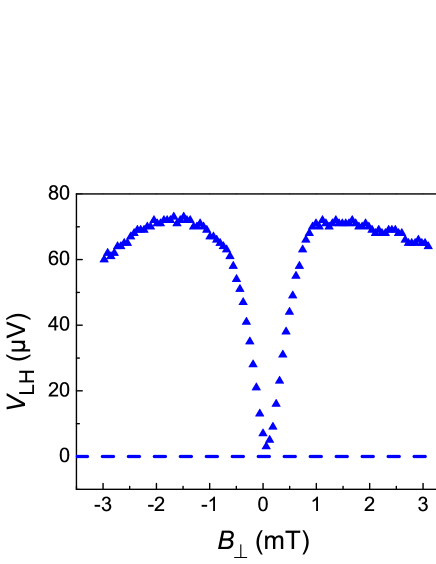
The spin signal in the local configuration (V) is larger than that in the non-local one (V) by a factor of about 18. This observation is in contrast to a one-dimensional spin diffusion model, where an expected ratio of has been experimentally verified.Jedema et al. (2003) A deviation from this factor has been observed previously in FM/semiconductor hybrid systems and explained by an increase of the spin diffusion length in the local case due to the electric field in the semiconductor,Sasaki et al. (2011) possibly due to an increase of as shown above. Similar to the NL case (cf. inset of Fig. 2), we measured the dependence of on the separation and obtained indeed an increased spin diffusion length of m. Taking into account the different spin diffusion lengths, the ratio has to be corrected by a factor of due to the different values of in Eq. (1). As a result, the corrected ratio is still about a factor of larger than expected according to the theory for a one-dimensional spin diffusion model.Fert and Lee (1996); Jedema et al. (2003) This remaining enhancement of the local spin valve signal might be related to the predicted half-metallic nature of Co2FeSi in its L21 phase. More precisely, the large spin polarization at the Fermi energy in Co2FeSi may lead to a comparatively large spin detection efficiency in the local spin valve configuration.
We have presented unambiguous evidence for all-electrical spin injection and detection in the local and non-local configuration in the Co2FeSi/GaAs hybrid system. The obtained magnetoresistance for the local spin valve configuration is found to be in accordance with the calculated estimate for (non-optimized) device parameters. The enhanced LSV signal with respect to the NL one suggests that the large spin polarization of Co2FeSi in the well-ordered L21 phase is advantageous for actual spintronic devices.
Acknowledgements.
We gratefully acknowledge the technical support by Walid Anders and Angela Riedel and the critical reading of the manuscript by Alberto Hernández-Mínguez.References
- Datta and Das (1989) S. Datta and B. Das, Appl. Phys. Lett. 56, 665 (1989).
- Sugahara and Tanaka (2004) S. Sugahara and M. Tanaka, Appl. Phys. Lett. 84, 2307 (2004).
- Johnson and Silsbee (1985) M. Johnson and R. H. Silsbee, Phys. Rev. Lett. 55, 1790 (1985).
- Jedema, Filip, and van Wees (2001) F. J. Jedema, A. T. Filip, and B. J. van Wees, Nature 410, 345 (2001).
- Tang et al. (2002) H. X. Tang et al., Semicondoctor Spintronics and Quantum Computation, edited by D. D. Awschalom, D. Loss, and N. Samarth (Springer, 2002).
- Wurmehl et al. (2005) S. Wurmehl, G. H. Fecher, H. C. Kandpal, V. Ksenofontov, C. Felser, H.-J. Lin, and J. Morais, Phys. Rev. B 72, 184434 (2005).
- Bruski et al. (2011) P. Bruski, S. C. Erwin, M. Ramsteiner, O. Brandt, K.-J. Friedland, R. Farshchi, J. Herfort, and H. Riechert, Phys. Rev. B 83, 140409(R) (2011).
- Hashimoto et al. (2005a) M. Hashimoto, J. Herfort, H.-P. Schönherr, and K. H. Ploog, Appl. Phys. Lett. 87, 102506 (2005a).
- Ramsteiner et al. (2008) M. Ramsteiner, O. Brandt, T. Flissikowski, H. T. Grahn, M. Hashimoto, J. Herfort, and H. Kostial, Phys. Rev. B 78, 121303 (2008).
- Hashimoto et al. (2005b) M. Hashimoto, J. Herfort, H.-P. Schönherr, and K. H. Ploog, J. Appl. Phys. 98, 104902 (2005b).
- Hashimoto et al. (2007) M. Hashimoto, A. Trampert, J. Herfort, and K. H. Ploog, J. Vac. Sci. Technol. B 25, 1453 (2007).
- Kasahara et al. (2012) K. Kasahara, Y. Baba, K. Yamane, Y. Ando, S. Yamada, Y. Hoshi, K. Sawano, M. Miyao, and K. Hamaya, J. Appl. Phys. 111, 07C503 (2012).
- Jönsson-Åkerman et al. (2000) B. J. Jönsson-Åkerman, R. Escudero, C. Leighton, S. Kim, I. K. Schuller, and D. A. Rabson, Appl. Phys. Lett. 77, 1870 (2000).
- Salis, Fuhrer, and Alvarado (2009) G. Salis, A. Fuhrer, and S. F. Alvarado, Phys. Rev. B 80, 115332 (2009).
- Johnson (1993) M. Johnson, Phys. Rev. Lett. 70, 2142 (1993).
- Jedema et al. (2003) F. J. Jedema, M. S. Nijboer, A. T. Filip, and B. J. van Wees, Phys. Rev. B 67, 085319 (2003).
- Fabian et al. (2007) J. Fabian, A. Matos-Abiaguea, C. Ertlera, P. Stano, and I. Žutić, Acta Physica Slovaca 57, 565 (2007).
- Lou et al. (2007) X. Lou, C. Adelmann, S. A. Crooker, E. S. Garlid, J. Zhang, K. S. M. Reddy, S. D. Flexner, C. J. Palmstrøm, and P. A. Crowell, Nat. Phys. 3, 197 (2007).
- Ciorga et al. (2009) M. Ciorga, A. Einwanger, U. Wurstbauer, D. Schuh, W. Wegscheider, and D. Weiss, Phys. Rev. B 79, 165321 (2009).
- Salis et al. (2010) G. Salis, A. Fuhrer, R. R. Schlittler, L. Gross, and S. F. Alvarado, Phys. Rev. B 81, 205323 (2010).
- Jedema et al. (2002) F. J. Jedema, H. B. Heersche, A. T. Filip, J. J. A. Baselmans, and B. J. van Wees, Nature 416, 713 (2002).
- Fert and Jaffrès (2001) A. Fert and H. Jaffrès, Phys. Rev. B 64, 184420 (2001).
- Dery, Cywiński, and Sham (2006) H. Dery, L. Cywiński, and L. J. Sham, Phys. Rev. B 73, 041306 (2006).
- Fert et al. (2007) A. Fert, J. M. George, H. Jaffres, and R. Mattana, IEEE Transactions on Electron Devices 54, 921 (2007).
- Schmidt et al. (2000) G. Schmidt, D. Ferrand, L. W. Molenkamp, A. T. Filip, and B. J. van Wees, Phys. Rev. B 62, R4790 (2000).
- Ando et al. (2010) Y. Ando, K. Kasahara, K. Yamane, K. Hamaya, K. Sawano, T. Kimura, and M. Miyao, Applied Physics Express 3, 093001 (2010).
- Ciorga et al. (2011) M. Ciorga, C. Wolf, A. Einwanger, M. Utz, D. Schuh, and D. Weiss, AIP Advances 1, 022113 (2011).
- Nakane et al. (2010) R. Nakane, T. Harada, K. Sugiura, and M. Tanaka, Jap. J. Appl. Phys. 49, 113001 (2010).
- Sasaki et al. (2011) T. Sasaki, T. Oikawa, T. Suzuki, M. Shiraishi, Y. Suzuki, and K. Noguchi, Appl. Phys. Lett. 98, 262503 (2011).
- Althammer et al. (2012) M. Althammer, E.-M. Karrer-Müller, S. T. B. Goennenwein, M. Opel, and R. Gross, Appl. Phys. Lett. 101, 082404 (2012).
- Fert and Lee (1996) A. Fert and S.-F. Lee, Phys. Rev. B 53, 6554 (1996).