Periodicity of resonant tunneling current induced by the Stark resonances in semiconductor nanowire
Abstract
The modification of the electronic current resulting from Stark resonances has been studied for the semiconductor nanowire with the double-barrier structure. Based on the calculated current-voltage characteristics we have shown that the resonant tunneling current is a periodic function of the width of the spacer layer. We have also demonstrated that the simultaneous change of the source-drain voltage and the voltage applied to the gate located near the nanowire leads to almost periodic changes of the resonant tunneling current as a function of the source-drain and gate voltages. The periodic properties of the resonant tunneling current result from the formation of the Stark resonance states. If we change the electric field acting in the nanowire, the Stark states periodically acquire the energies from the transport window and enhance the tunneling current in a periodic manner. We have found that the separations between the resonant current peaks on the source-drain voltage scale can be described by a slowly increasing linear function of the Stark state quantum number. This allows us to identify the quantum states that are responsible for the enhancement of the resonant tunneling. We have proposed a method of the experimental observation of the Stark resonances in semiconductor double-barrier heterostructures.
pacs:
73.21.Hb, 73.63.NmI Introduction
The Wannier-Stark resonance states have been attracting substantial interest for many years.Wannier1962 ; Wilkinson1996 ; Morifuji1997 ; Gluck2002 ; Rosam2003 These states are created if the electron is simultaneously subjected to a periodic field, e.g., of the crystal or the superlattice, and to a uniform electric field.Gluck2002 ; bookSchafer2002 The joint effect of these fields leads to the formation of the Wannier-Stark states that exhibit the double periodicity, namely, the periodic localization in the real space and the periodic sequence of energy levels.Gluck2002 The Wannier-Stark states have been observed experimentally in semiconductor superlattices by measuring the Zener tunneling current.Morifuji1997 The lifetime of the Wannier-Stark resonances has been studied both experimentally and theoretically by Rosam et al.Rosam2003 The Wannier-Stark resonances have been also observed in the optical lattices, e.g., for the system of cold atoms in the accelerated standing laser wave.Wilkinson1996 Recently, the essential progress has been reported both in the experimentalSobolev2010 ; Lima2010 ; Tackmann2011 and theoreticalKolovsky2013 studies of these states,
Similar resonance states can be formed if the uniform electric field is applied to a semiconductor quantum-well heterostructure.Austin1985 ; Ahn1986 ; Austin1988 Since the periodic field is not necessary to the formation of these states, as it was demonstrated for isolated quantum wellsAustin1985 ; Ahn1986 and aperiodic structuresSpisak2009PRB , they are called the Stark resonances. The Stark resonances can also occur in the double-barrier resonant tunneling structures under an external electric field.Peng1991 ; Niculescu2000 The effect of the electric field on the energy of the Stark resonances and on the resonance lifetimes has been studied theoretically for a single quantum wellAustin1985 ; Ahn1986 ; Borondo1986 and for double-barrier structures.Peng1991 ; Porto1994 ; Bylicki1996 ; Niculescu2000 ; Zambrano2002 One can expect that the Stark resonances will be observed in the measurements of the current-voltage characteristics of the devices containing the double-barrier structures, which can be fabricated either in mesa-type layer structures or in nanowires.Bjork2002
The electronic transport in the double-barrier structures embedded in nanowires has been studied experimentally in Refs. Bjork2002, ; Fuhrer2007APL, ; Fuhrer2007NL, ; Pfund2007, . The theory of the coherent electronic transport in nanowires with Gaussian-type scatterers has been elaborated in the papers.Bardarson2004 ; Gudmundsson2008 The modification of the electron transport in the nanowire due to the quantum ring, dot, and barrier has been studied by Gudmundsson et al.Gudmundsson2005 In Ref. Sowa2010, , the current-voltage characteristics of the nanowire with the embedded double-barrier structure have been determined for different spacer widths. It has been shownSowa2010 that the resonant current peak possesses the asymmetric Fano-type shape for the sufficiently narrow spacers.
In the present paper, we focus on the effect of the spacer width and the source-drain and gate voltages on the resonant tunneling current through a semiconductor nanowire containing a double-barrier structure. We demonstrate that the resonant current peaks periodically change their heights if we change the spacer width and/or source-drain voltage with the suitably tuned gate voltage. This periodicity results from the formation of the Stark resonance states.
II Theory
We study the electron transport in the semiconductor nanowire with the double-barrier structure (Fig. 1). In an external uniform electric field acting parallel to the nanowire axis, the electronic current can be described within the effective mass approximation by the one-dimensional (1D) model. We consider the circuit with the source (S) and drain (D) contacts attached to both the ends of the nanowire. Voltages and applied to these contacts result in the source-drain voltage that generates the uniform electric field , where and is the the length of the nanowire, i.e., the source-drain distance. The source and drain contacts are made from the heavily doped semiconductors. Throughout the present paper, the energy of the conduction band bottom of the source is taken as the reference energy and put equal to zero, moreover, we take on . In the calculations, we also include the effect of the side gate electrode assumed to be a ring surrounding the nanowire in the region of the central quantum well (CQW). If voltage is applied to the gate, the potential energy of the bottom of the CQW is changed by , where is the voltage-to-energy conversion factor.bookAdamowski2006
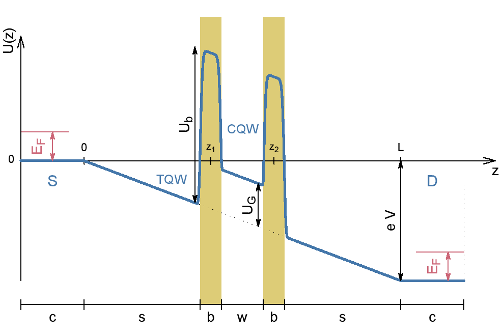
We consider the nanowire that consists of the CQW with width surrounded by the two barriers of equal width that are separated from the contacts by the spacers of the same width , i.e., . The potential energy (Fig. 1)
| (1) |
is the sum of the double-barrier potential energy and the potential energy of the electron in electric field of finite range , where
| (2) |
The double-barrier potential energy is taken on in the form of the two-center power-exponential functionCiurla2002 ; Kwasniowski2008
| (3) |
where the height of the barriers, , is measured with respect to the energy of the nearby regions of the spacers. Parameter describes the sharpness of the interfaces: for we obtain the soft Gaussian potentials, while for we get the two rectangular barriers of width centered at and .
Electronic current is calculated within the Landauer formalism using the relationbookDiVentra2008
| (4) |
where is the transmission coefficient. The electrons in the contacts are described by the Fermi-Dirac distribution function
| (5) |
where and are the electrochemical potentials of the source and drain, respectively. We calculate by the transfer matrix method with potential energy (1) approximated by a piecewise constant function.
In order to focus on the effects of geometry and external voltages on the electronic current, we have performed the calculations for and neglected the electron scattering. At zero temperature, the distribution functions (5) become the simple step functions with the electrochemical potentials and , where the Fermi energy, , is assumed to be the same for the source and drain. In this case, the integration in Eq. (4) runs over the transport window of width and can be performed numerically.
The numerical calculations have been performed for the InAs nanowire with the InP barriersBjork2002 for the fixed values of the following material parameters: eV, nm (hence nm), nm, and meV. Because the widths of the InP barriers are much smaller than length of the nanowire, we assume that the electrons are described by the InAs conduction-band mass, i.e., we take on , where is the free-electron rest mass. Putting 6 we account for the observed non-perfect sharpness of the InAs/InP interfaces.Bjork2002 ; Niquet2008 ; Thelander2004 However, we have found that the calculated current-voltage characteristics are rather insensitive to the variation of provided that the potential-energy profile is sufficiently steep at the interface. Therefore, the periodic behavior of the resonant current peaks presented in Sec. III is the same for , i.e., for the rectangular potential barriers and well.
We have calculated the current-voltage characteristics using Eq. (4) for different spacer widths , i.e., for the nanowires with different lengths . Due to the geometric symmetry of the nanodevice the change of the spacer width by corresponds to the change of the length of the nanowire by . In order to carry out the transfer-matrix calculations, we have introduced the -coordinate mesh with mesh points in the interval . has been chosen in such a manner that the minimal distance between the nearest mesh points on the -axis is equal to nm, which gives, e.g., for nm.
III Results
A. Periodicity of resonant current peaks
The present calculations are based on the following physical background: at zero temperature the incident electron with energy can tunnel from the source to the drain through the double-barrier heterostructure in a resonant tunneling process if energy is aligned with energy of quasi-bound state localized in the CQW and both the energies fall into the transport window, i.e.,
| (6) |
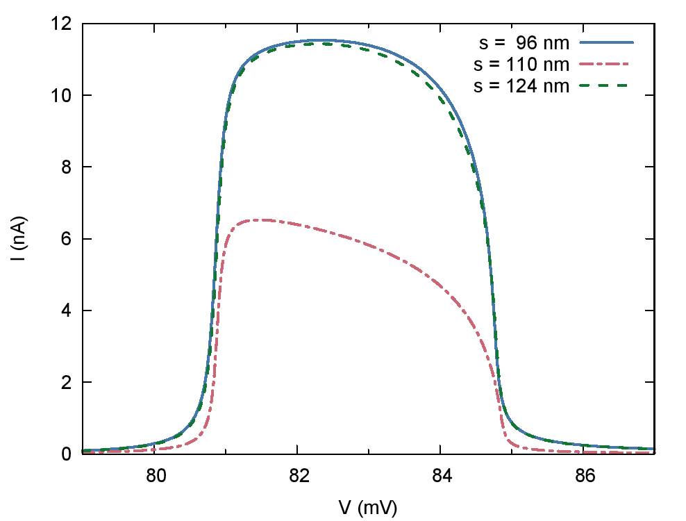
If condition (6) is satisfied, then – for suitably chosen spacer width – we obtain the strong resonant tunneling current peak on the current-voltage characteristics that takes on the shape typical for the resonant tunneling diodeSowa2010 (solid, blue curve in Fig. 2). However, if we perform the calculations for the spacer that is wider by nm, the current peak becomes weak, i.e., its height is smaller by a factor of two in comparison to the height of the strong peak. After increasing the spacer width by , the current-voltage characteristics with the strong resonant peak is recovered (Fig. 2). We have found that the similar sequence of the strong and weak resonant current peaks is repeated every time, if we increase or decrease the spacer width by the same period of approximately 28 nm. The periodic changes of the resonant current peaks are presented in Fig. 3.
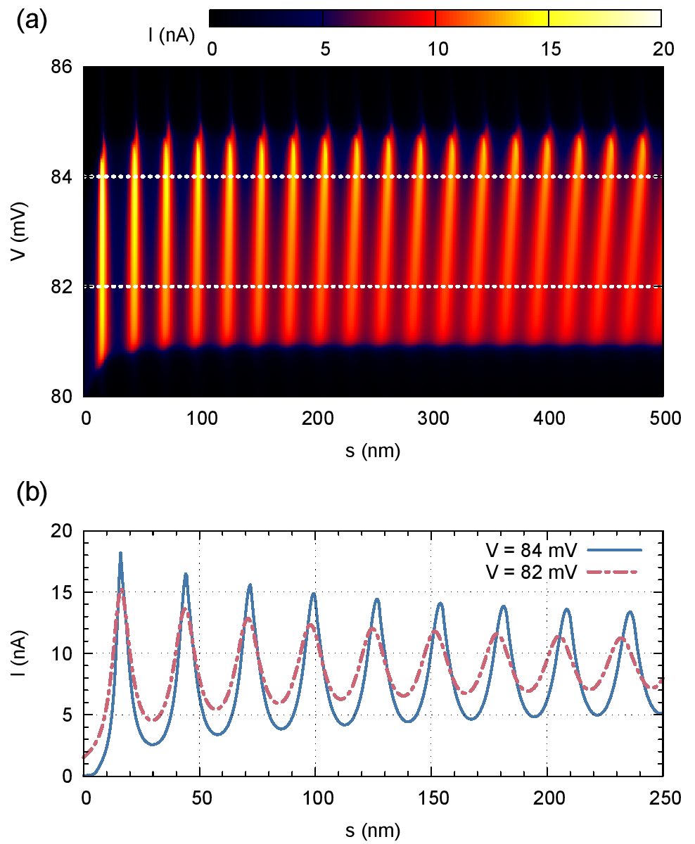
Fig. 3(a) displays the resonant current peak that spreads from mV to mV on the current-voltage characteristics. This peak results from the resonant tunneling via the lowest-energy level meV that satisfies the resonant-tunneling condition (6). If we change the spacer width, i.e., the source-drain separation, the resonant tunneling current changes considerably. Fig. 3(b) shows that the resonant tunneling current peaks change periodically with the spacer width. Based on these results we have estimated that the subsequent strong/weak resonant current peaks are separated by nm. Fig. 3(b) also shows that – for mV – the strong resonant current peak is 3-5 times higher than the weak resonant current peak. The largest difference between the strong and weak peaks can be observed for the narrow spacers, i.e., for nm.
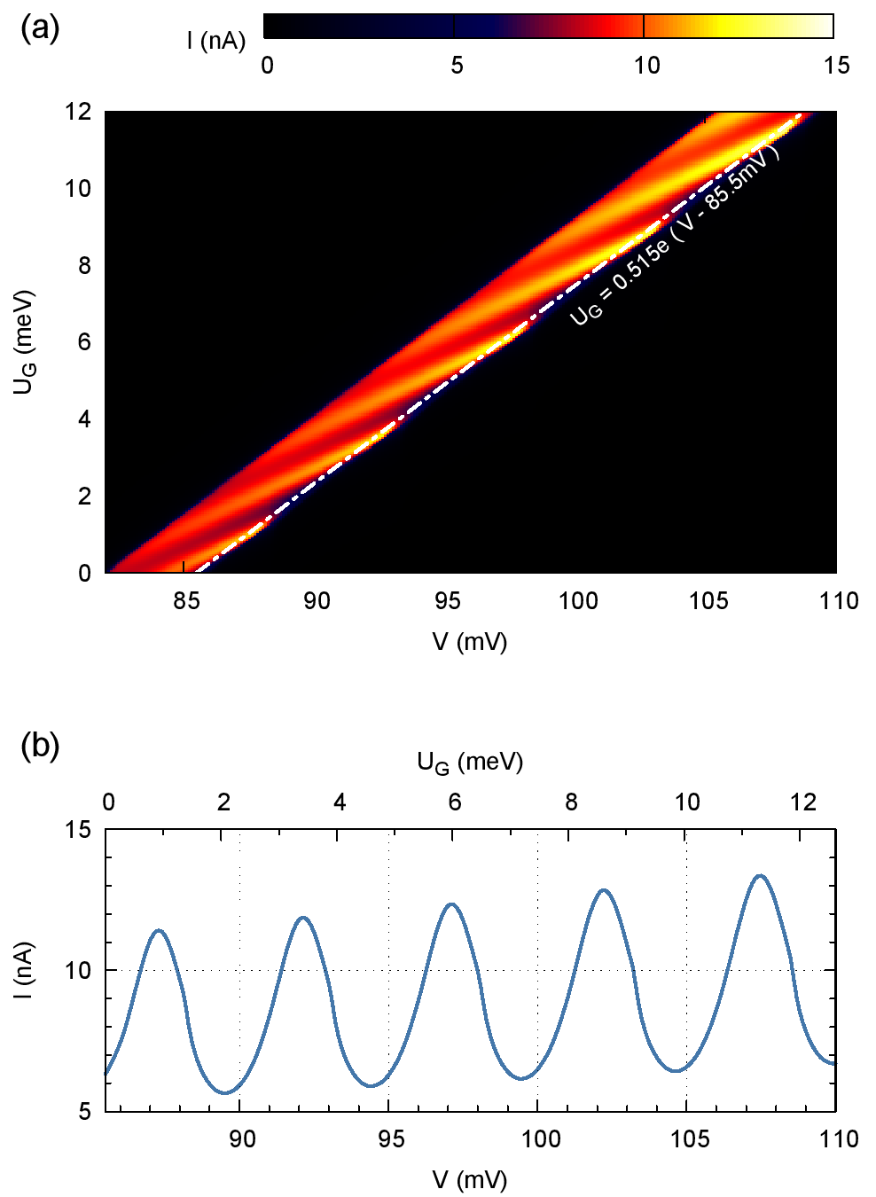
There appears a question if can we modify the periodicity of the resonant current flowing through the nanowire by applying the additional voltage to the side gate? In order to answer this question, we have simulated the effect of gate voltage by shifting the CQW potential energy bottom by (cf. Fig. 1). Since the actual value of depends on the parameters of the nanostructure and also on the gate voltage,bookAdamowski2006 we have used in the calculations – instead of the gate voltage – the suitably chosen values of potential energy shift . The results are depicted in Fig. 4. For the negative gate voltage and for the potential energy changes by , which shifts upwards the energy levels of the quasi-bound states localized in the CQW. This in turn causes that the resonant tunneling condition (6) is no longer satisfied, i.e., the resonant tunneling is broken. Therefore, in order to recover the resonant tunneling we have to change the source-drain voltage in an appropriate manner. We have found that changing simultaneously the voltages and according to the relation
| (7) |
where mV, allows us to follow the maxima of the resonant tunneling current and its periodic changes (Fig. 4). Prefactor 0.515 is the lever factor for the source-drain voltage. Its value (slightly larger than the value 0.5, which is appropriate for the ideally symmetric system) accounts for a slight asymmetry of the nanodevice due to the electric field acting between the source and the drain. If the gate voltage is changed in such a way that increases from 0 to 10 meV, the position of the resonant current peak on the current-voltage characteristics is shifted from mV to mV (Fig. 4). The corresponding sequence of the resonant current peaks is visible along the stripe on Fig. 4(a). Fig. 4(b) shows that the height of the resonant tunneling current peak changes by a factor of two if the source-drain and gate voltages are varied according to Eq. (7), i.e., along the straight line displayed on Fig. 4(a). We have estimated the average separation between the neighboring strong peaks to be mV, which corresponds to the change of the CQW potential energy by meV. We note that the almost periodic changes of the height of the resonant current peak depicted in Fig. 4 have been obtained for the fixed geometric parameters of the nanodevice, in this case, for nm and nm.
However, after a closer inspection of the results shown in Fig. 4(b) we have found that – on the contrary to the constant separation between the strong resonant tunneling current peaks as a function of the spacer width [Fig. 3(b)] – the separations between the current peaks [Fig. 4(b)] slightly increase with the increasing source-drain voltage. This effect will be explained in Section IV.
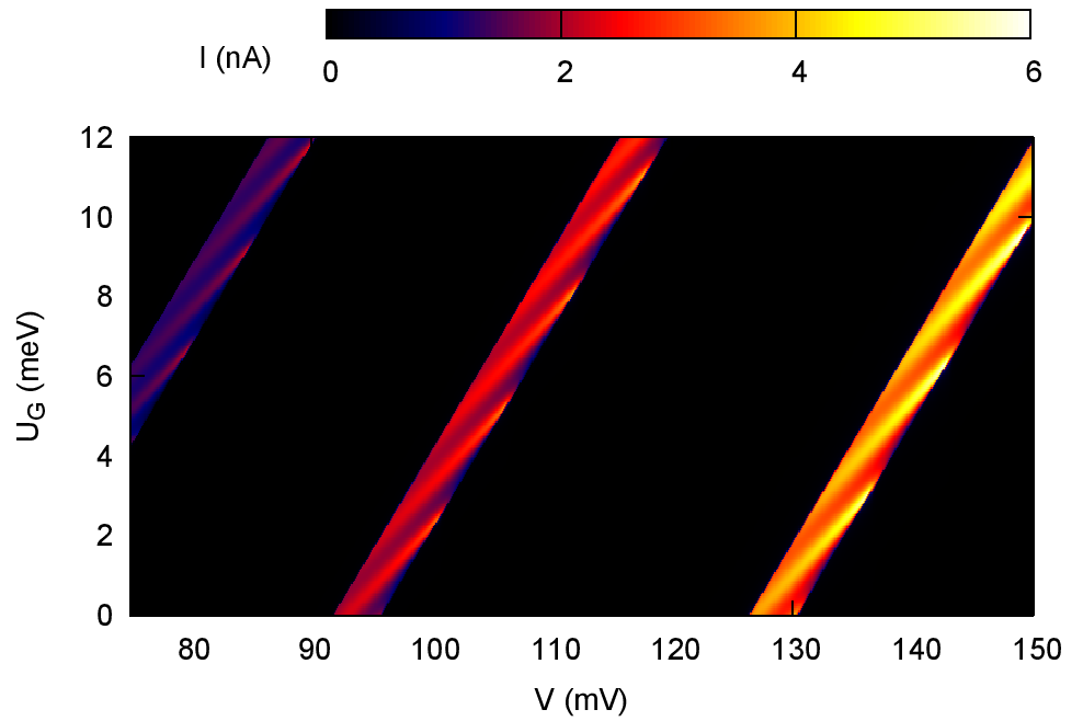
The width of the side gate, to which voltage is applied, should be approximately equal to width of the CQW. In the recently fabricated nanodevices,Tomioka2012 the ring-shaped gates that surround the nanowires are much wider than that used to obtain the results presented in Fig. 4. In order to check if the periodic behavior of the resonant current peaks also occurs for the wider gates and CQW’s, we have performed the calculations for nm. The results are displayed in Fig. 5. We have found that the periodic sequence of the strong and weak resonant current peaks is still visible when the gate voltage is changed with the increasing bias voltage according to formula (7). As opposite to the narrow CQW (Fig. 4), we obtain more than one resonant current peak within the same range of the source-drain voltage, which results from the fact that for the wider CQW energy levels possess the lower energies and the energy separations between them are smaller. Therefore, more than one CQW energy level enters the transport window in the considered source-drain voltage range. In Fig. 5, this effect is shown as the three stripes that correspond to the three states with subsequent energy levels The direct numerical calculation of energy levels has allowed us to identify these quantum states as described by quantum numbers .
B. Stark resonances
In order to find the physical interpretation of the periodic behavior of the resonant tunneling current, we have analyzed the transmission coefficient as a function of the spacer width and the source-drain voltage. The corresponding plots are presented in the upper parts of Figs. 6 and 7. In the lower parts of these figures, we plot energy levels of quasi-bound states localized in the triangular quantum well (TQW) that is formed in the left spacer due to the uniform external electric field acting parallel to the nanowire axis. Energy levels have been calculated by the second-order finite-difference method by diagonalizing the resulting Hamiltonian matrix in the computational box expanded by to the right and to the left from the right and left spacer boundaries, respectively (cf. Fig. 1). In this way, we have checked that the physically relevant results do not depend on the size of the computational box. In Figs. 6 and 7, the gray and blue dots correspond to energy levels calculated with the expanded computational box. The majority of the quantum states associated with these energy levels are the states localized in the right contact. The energy levels associated with these states are marked by the gray dots in the lower parts of Figs. 6 and 7 [see also Fig. 8(b)]. These states are the eigenstates of the system with the potential-energy profile, which includes the flat potential energy regions corresponding to the contacts (cf. Fig. 1), and result from the binding of the electron in the computational box of finite size, i.e., they are unphysical. However, the fact that we have obtained these states proves the reliability of the finite difference method applied and means that we have not omitted any eigenstates of the system in the calculations. The physical meaning can be attributed to the states with the energy levels depicted by the blue dots in Figs. 6 and 7, which form almost vertical lines in Fig. 6. The energy levels plotted by the blue dotted curves in Figs. 6, 7, and 8(b) have been calculated for the simplified shape of the potential energy shown by the blue solid lines in Fig. 8(a). It is interesting that these energy levels exactly agree with those calculated for the entire system with the double-barrier potential (the gray dots along the blue curves are not visible since they coincide with each other). The results of the calculations with the potential energy represented by only the left part of the potential-energy profile allow us to interpret the physically relevant energy levels as associated with the quasi-bound states localized in the TQW in the left spacer region.
We see that both the transmission coefficient and the energy levels are periodic functions of spacer width for fixed (Fig. 6) or the source-drain voltage and gate voltage for fixed (Fig. 7). Using Eq. (4) we can state that the periodicity of the transmission coefficient leads to the periodicity of the resonant tunneling current. The estimated average values of periods and almost exactly coincide with the periods of the strong/weak resonant current peak sequence estimated from Figs. 3 and 4. For (Fig. 6) the subsequent maxima of the transmission coefficient appear for the energy of the incident electrons meV. This energy is aligned with the lowest-energy level of the quasi-bound state localized in the CQW for mV. Along the straight line the transmission coefficient as a function of spacer width periodically reaches the value , which demonstrates that we deal with the resonant tunneling effect with the periodic changes of the transmission. Only for the narrow spacers with nm the maximum of transmission coefficient becomes smaller than 1 and is shifted towards the lower energy values.Sowa2010
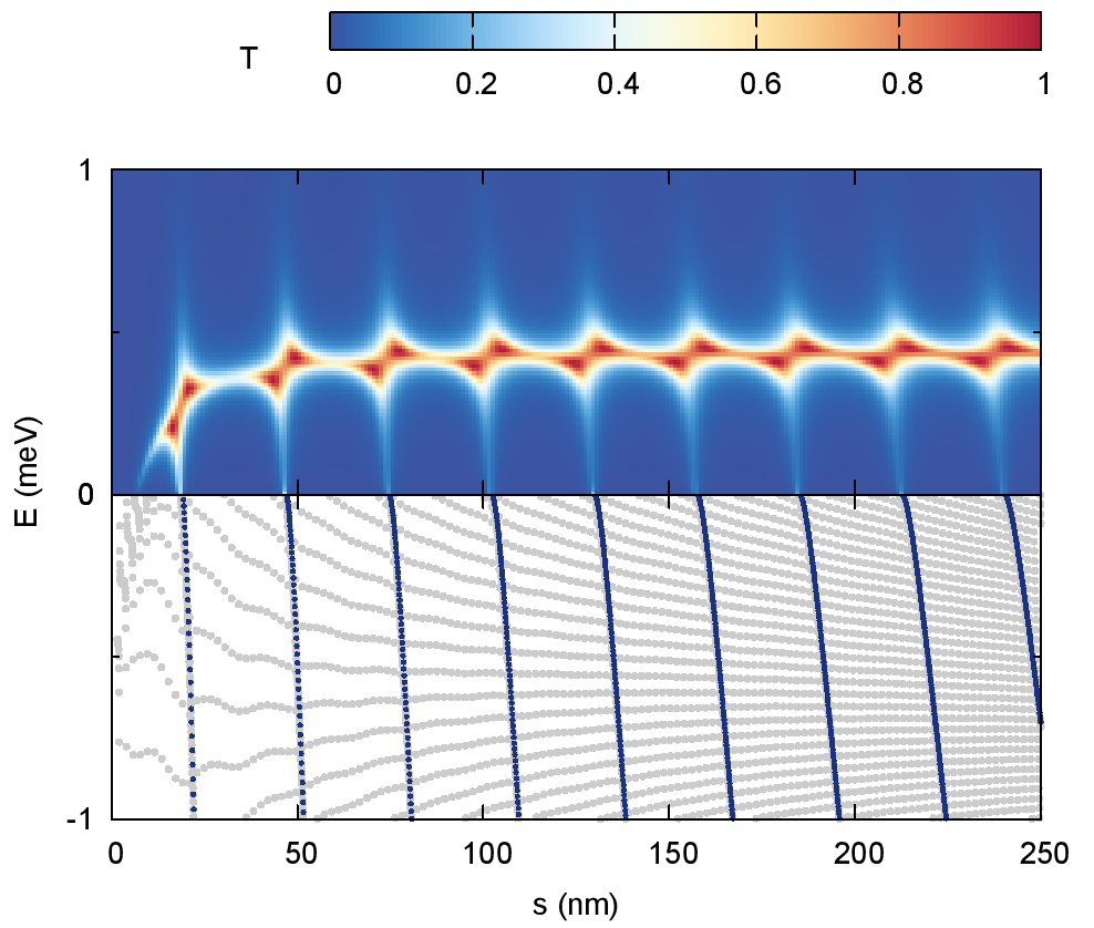
If the spacer width decreases, the (negative) energy of the quasi-bound state increases reaching and continuously goes over into the curve corresponding to the energy of the resonance state with . The transmission maxima correspond to the resonance states with energies and finite widths that are clearly visible on Fig. 6.
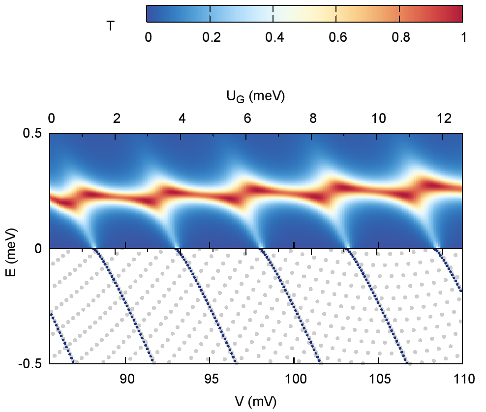
Of course, the same mechanism is responsible for the creation of the resonances when the geometric sizes of the device are fixed, but the source-drain voltage is changed together with the gate voltage according to formula (7). Fig. 7 displays the outcome of the similar calculations as in Fig. 6, but now the source-drain voltage is altered at fixed , which shifts the energy levels of the quasi-bound states localized in the CQW. Therefore, in order to satisfy the resonant tunneling condition we have to compensate this shift by applying the suitably chosen gate voltage. The increasing source-drain voltage causes that the depth of the TQW generated in the left spacer also increases, which leads to the growth of the number of the quasi-bound states localized in the TQW.
IV Discussion
Based on the results presented in Figs. 6 and 7 we can give the physical interpretation of the periodicity of the resonant tunneling current peaks. If spacer width (Fig. 6) or source-drain voltage (Fig. 7 ) decrease, quasi-bound state localized in the TQW gains the energy until it becomes unbound and goes over into the resonance state with the positive energy. Figs. 6 and 7 demonstrate that the formation of the resonance states is periodically repeated when changing or .
The resonant tunneling condition in the conventional form (6) neglects the formation of Stark resonances. If we take these states into account, condition (6) is modified to
| (8) |
where is the real part of the energy of the -th Stark resonance. The upper panels in Figs. 6 and 7 show that the transmission is periodically enhanced by the contributions arising from the Stark resonance states. Based on the modified resonant tunneling condition (8) we propose the following description of the resonant tunneling: the electrons injected from the source form the Stark resonance states in the TQW in the left spacer. If the energy of the Stark resonance is aligned with the energy of the quasi-bound state in the CQW, the electrons can tunnel through the nanowire with the transmission coefficient 1. This means that the resonant tunneling involves the two states: the Stark resonance in the TQW and the quasi-bound state in the CQW. The similar two-step tunneling have been studied in our previous paper,Wojcik2010 in which we have found the intrinsic oscillations of the current in the triple-barrier resonant tunneling diode.
The separations, measured on the spacer width scale (Fig. 6) and on the voltage scale (Fig. 7), between the subsequent Stark resonances and also between the corresponding quasi-bound states localized in the TQW are almost equal to each other. The strong resonant tunneling peaks appear for the Stark resonances with the energies slightly larger than zero.
We note that in both the considered cases, i.e., (i) change of the spacer width at the constant source-drain voltage and (ii) simultaneous change of the source-drain and gate voltages at the constant spacer width, we are dealing with the changes of the effective electric field acting in the nanostructure, since in case (i) the change of spacer width is equivalent to the change of electric field .
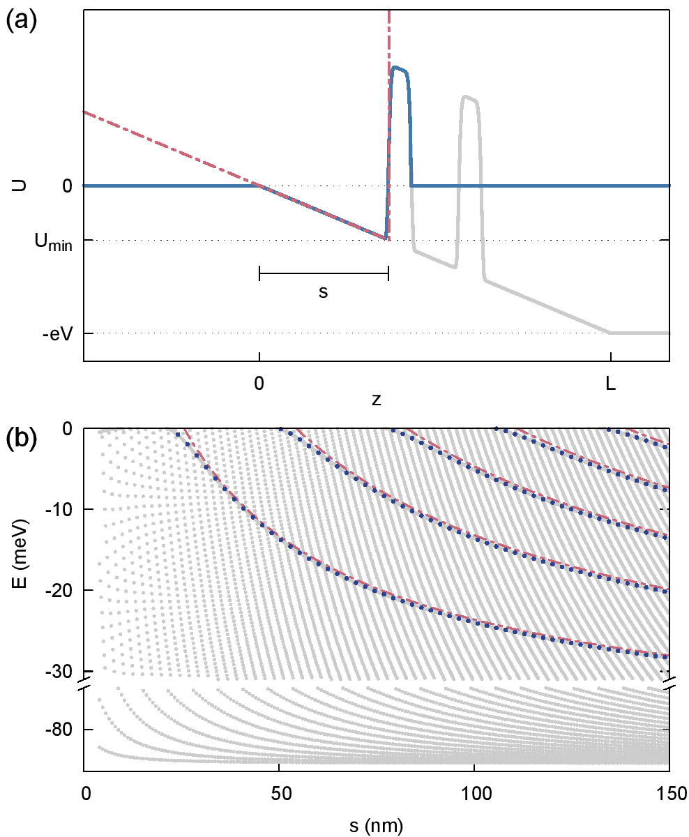
The previous part of the discussion was based on the numerical results. In the following part, we will reach the same conclusions based on the analytical calculations. For this purpose we propose a simple model that – in spite of its simplicity – includes the essential physics of the considered nanosystem. The Stark states are formed in the TQW in the left spacer region. Therefore, we construct the simplified potential energy profile (blue curve in Fig. 8) including the triangular potential and the left potential barrier only, which accurately approximates the corresponding part of potential energy plotted in Fig. 1. In order to obtain the analytical results, we make the further approximation and assume that the triangular potential possesses the infinite depth and range but the same slope (determined by the electric field ) as the original potential energy in the left spacer region (red dash-dotted lines in Fig. 8). Minimal value of the potential energy (Fig. 8) is determined by width of the left spacer, i.e., .
In this case, the energy eigenvalues for the infinite triangular potential can be written asbookDavies1998
| (9) |
where and is the -th zero of the Airy function . Quantities can be approximated by the formulabookAbramowitz1974
| (10) |
which leads to very accurate estimates of the exact values. The relative errors of estimates (10) are very small and decrease with , taking on the values , , for , respectively.bookAbramowitz1974
We apply Eqs. (9) and (10) to the infinite TQW that approximates the potential energy of the left spacer with width and obtain
| (11) |
where . Fig. 8(b) shows that the energy levels calculated from Eq. (11) for the infinite triangular potential (red dash-dotted lines) and calculated by the numerical method for the the simple model with the left spacer and barrier (blue dots) and for the the full potential-energy profile (gray dots) almost exactly agree with themselves.
Neglecting the small positive shift of the resonance energy (cf. upper parts of Figs. 6 and 7), we can assume that the maximum of the resonant tunneling current appears if the Stark state localized in the left spacer becomes unbound and goes over into the Stark resonance. Then, the resonant tunneling condition takes on the following approximate form:
| (12) |
Using Eqs. (11) and (12) we have determined the spacer width , for which resonant tunneling condition (12) is satisfied. This leads to
| (13) |
The numerical solutions of Eq. (13) for mV and results in nm and nm. These intervals are nearly equal to each other and agree very well with the differences between the spacer widths that correspond to the subsequent strong peaks of the resonant tunneling current obtained from the extended numerical calculations [cf. Fig. 3(b)].
If , the left hand side of Eq. (13) can be approximated by , from which we obtain
| (14) |
The differences between the spacer widths corresponding to the neighboring strong resonant current peaks are given by
| (15) |
Formula (15) demonstrates that the separations between the subsequent resonant current peaks are periodic functions of the spacer width and are independent of . For mV, we obtain from Eq. (15) nm, which again is in a good agreement with the estimates obtained from Eq. (13) and with the results of Fig. 3(b).
Eq. (11) can also be applied to estimate the values of the source-drain voltage that correspond to the strong resonant current peaks (Fig. 4). Using condition (12) we obtain
| (16) |
where . Inserting into Eq. (16) the values of the parameters used in Fig. 4 we get mV and 4.82, 4.95, 5.08, and 5.20 mV for , and , respectively. These values agree very well with the numerical estimates (4.85, 4.99, 5.12, and 5.23 mV) obtained for the same states from Fig. 4(b). According to Eq. (16) the separations between the subsequent strong resonant current peaks on the source-drain voltage scale slowly increase with and can be described by the linear function of . We remind that is the quantum number of the Stark state. Formula (16) allows us to reproduce the results of the time-consuming computer simulations in a simple way. Due to the high accuracy of the results obtained from (16) this formula can be used to ascribe the value of quantum number to the considered state, which means that we have a tool to identify the Stark resonance state that is responsible for the given strong resonant current peak. The analytical results (15) and (16) provide an additional explanation of the periodic behavior of the resonant tunneling current presented in Sec. III.
We would like to comment on the use of notation and for the one-electron energy levels. These symbols denote the energy levels of one-electron states and , respectively, that are the eigenstates of the electron with the potential energy depicted in Fig. 1. However, both the numerical and analytical results (11) show that the states and are localized in the two different parts of the nanostructure, namely, states are localized in the TQW in the left spacer region and states are localized in the CQW. Therefore, it is convenient to denote these two subsets of quantum states of the same system by the different quantum numbers and .
We have also found that the periodic properties of the resonant current peaks presented in Sec. III can be obtained within the three-dimensional (3D) model of the nanowire, i.e., can be observed in the realistic nanowires.Bjork2002 The results of our preliminary calculations performed with the use of the adiabatic approximation show that the resonant current peaks are periodic functions of the spacer width and source-drain voltage. The present results can be directly applied to the 3D nanowire if zero on the energy scale is taken at the ground-state energy of the state that results from the spatial quantization of the lateral electron motion, i.e., the motion in the plane. We note that the present 1D model of the electron transport can also be applied to the mesa-type resonant tunneling structures, for which we can assume the translational symmetry in the plane and separate the electron motion in the direction.
In the semiconductor nanowires, the influence of the impurities on the electron transport should be taken into account, since the spacer regions with the sufficiently high purity can hardly be fabricated. In the present work, we have neglected the electron-impurity scattering. Moreover, in the -doped nanowires, the ionization of donors generates the charge that can be accumulated in the source-related spacer region, which can change the potential profile and shift the energies of the Stark resonances. This in turn can disturb the resonant current peaks. However, in the moderately doped nanowire, due to its small lateral size only a small fraction of the charge will be gathered in the left spacer, which will not destroy the periodicity of the resonant current peaks.
V Conclusion
The results of the present paper show that the periodic patterns can be observed in the resonant tunneling current flowing through the double-barrier structures. The height of the resonant current peak is a periodic function of the spacer width. In other words, the resonant tunneling current exhibits periodic changes if the source-drain distance is changed. Moreover, the current peaks are periodic functions of the source-drain voltage if it is changed simultaneously with the voltage applied to the side gate. The similar periodicity can appear both in the semiconductor nanowires and in the resonant tunneling mesa structures. The physical interpretation of this periodicity is based on the formation of the Stark states in the triangular quantum well in the spacer region attached to the source contact. If the effective electric field becomes weaker, the quasi-bound Stark states localized in the triangular quantum well cease to be bound and go over into the resonance Stark states with the energies that enter the transport window. This process is periodically repeated when the spacer width and/or source-drain voltage are changed. The resonant tunneling current is periodically enhanced if the electrons tunnel from the source to drain via the Stark resonance state that is energetically aligned with the quasi-bound state in the CQW.
The Stark resonances, found in the present paper, are the analogues to the Wannier-Stark resonances predicted for the bulk crystals in external electric fieldWannier1962 and observed in semiconductor superlattices.Morifuji1997 It is interesting that the infinite triangular potential approximation very accurately describes the periodicity of the resonant current peaks, which allows us to explain the physical nature of this effect with the use of a simple analytically solvable model.
Based on the present results, we can propose a method of experimental observation of the Stark resonances in semiconductor double-barrier heterostructures that relies on the measurements of the current-voltage characteristics. The resonant current peaks that originate from the Stark resonances should exhibit the periodic behavior as a function of the spacer width, i.e., source-drain separation, for the constant source-drain voltage or as functions of source-drain and gate voltages for the nanowires with the fixed geometric parameters. We have found that the source-drain voltage difference corresponding to neighboring strong resonant tunneling current peaks is a linear function of the Stark state quantum number, which allows us to identify the Stark states in the double-barrier structures. We have also shown how to tune the external voltages applied to the double-barrier structures in order obtain the possibly large differences between the strong and weak resonant tunneling current peaks, i.e., to make the current periodicity measurable.
Acknowledgements.
This work has been supported by the National Science Centre, Poland, under grant No. DEC-2011/03/B/ST3/00240.References
- (1) G. H. Wannier, Rev. Mod. Phys. 34, 645 (1962).
- (2) S. R. Wilkinson, C. F. Bharucha, K. W. Madison, Q. Niu, and M. G. Raizen, Phys. Rev. Lett. 76, 4512 (1996).
- (3) M. Morifuji, K. Murayama, C. Hamaguchi, A. Di Carlo, P. Vogl, G. Böhm, and M. Sexl, phys. stat. sol. (b) 204, 368 (1997).
- (4) M. Glück, A. R. Kolovsky, and H. J. Korsch, Phys. Rep. 366, 103 (2002).
- (5) B. Rosam, K. Leo, M. Glück, F. Keck, H. J. Korsch, F. Zimmer, and K. Köhler, Phys. Rev. B 68, 125301 (2003).
- (6) W. Schäfer and M. Wegener, eds., “Semiconductor optics and transport phenomena,” (Springer, Berlin, 2002).
- (7) M. Sobolev, A. Vasil’ev, and V. Nevedomskii, Semiconductors 44, 761 (2010).
- (8) M. M. de Lima, Y. A. Kosevich, P. V. Santos, and A. Cantarero, Phys. Rev. Lett. 104, 165502 (2010).
- (9) G. Tackmann, B. Pelle, A. Hilico, Q. Beaufils, and F. Pereira dos Santos, Phys. Rev. A 84, 063422 (2011).
- (10) A. R. Kolovsky and E. N. Bulgakov, Phys. Rev. A 87, 033602 (2013).
- (11) E. J. Austin and M. Jaros, Phys. Rev. B 31, 5569 (1985).
- (12) D. Ahn and S. L. Chuang, Phys. Rev. B 34, 9034 (1986).
- (13) E. J. Austin and M. Jaros, Phys. Rev. B 38, 6326 (1988).
- (14) B. J. Spisak and M. Wołoszyn, Phys. Rev. B 80, 035127 (2009).
- (15) J.-P. Peng, H. Chen, and S.-X. Zhou, Phys. Rev. B 43, 12042 (1991).
- (16) A. Niculescu, in Semiconductor Conference, 2000. CAS 2000 Proceedings. International, Vol. 1 (IEEE, 2000) pp. 367–370.
- (17) F. Borondo and J. Sánchez-Dehesa, Phys. Rev. B 33, 8758 (1986).
- (18) J. A. Porto, J. Sánchez-Dehesa, L. A. Cury, A. Nogaret, and J. C. Portal, J. Phys. Condens. Matter 6, 887 (1994).
- (19) M. Bylicki, W. Jaskólski, and R. Oszwaldowski, J. Phys. Condens. Matter 8, 6393 (1996).
- (20) M. L. Zambrano and J. C. Arce, Phys. Rev. B 66, 155340 (2002).
- (21) M. T. Björk, B. J. Ohlsson, C. Thelander, A. I. Persson, K. Deppert, L. R. Wallenberg, and L. Samuelson, Appl. Phys. Lett. 81, 4458 (2002).
- (22) A. Fuhrer, C. Fasth, and L. Samuelson, Appl. Phys. Lett. 91, 052109 (2007).
- (23) A. Fuhrer, L. E. Fröberg, J. N. Pedersen, M. W. Larsson, A. Wacker, M.-E. Pistol, and L. Samuelson, Nano Letters 7, 243 (2007).
- (24) A. Pfund, I. Shorubalko, K. Ensslin, and R. Leturcq, Phys. Rev. Lett. 99, 036801 (2007).
- (25) J. H. Bardarson, I. Magnusdottir, G. Gudmundsdottir, C.-S. Tang, A. Manolescu, and V. Gudmundsson, Phys. Rev. B 70, 245308 (2004).
- (26) V. Gudmundsson, G. Thorgilsson, C.-S. Tang, and V. Moldoveanu, Phys. Rev. B 77, 035329 (2008).
- (27) V. Gudmundsson, Y.-Y. Lin, C.-S. Tang, V. Moldoveanu, J. H. Bardarson, and A. Manolescu, Phys. Rev. B 71, 235302 (2005).
- (28) A. Sowa-Rykowska and J. Adamowski, Phys. Rev. B 82, 195311 (2010).
- (29) J. Adamowski, S. Bednarek, and B. Szafran, “Handbook of semiconductor nanostructures and nanodevices,” (California: American Scientific Publisher, 2006) pp. 389–452, 1st ed.
- (30) M. Ciurla, J. Adamowski, B. Szafran, and S. Bednarek, Physica E 15, 261 (2002).
- (31) A. Kwaśniowski and J. Adamowski, J. Phys. Condens. Matter 20, 215208 (2008).
- (32) M. Di Ventra, Electrical Transport in Nanoscale Systems (Cambridge University Press, 2008).
- (33) Y.-M. Niquet and D. C. Mojica, Phys. Rev. B 77, 115316 (2008).
- (34) C. Thelander, M. Björk, M. Larsson, A. Hansen, L. Wallenberg, and L. Samuelson, Solid State Commun. 131, 573 (2004).
- (35) K. Tomioka, M. Yoshimura, and T. Fukui, Nature 488, 189 (2012).
- (36) P. Wójcik, B. J. Spisak, M. Wołoszyn, and J. Adamowski, Semicond. Sci. Technol. 25, 125012 (2010).
- (37) J. H. Davies, The Physics of Low-dimensional Semiconductors (Cambridge University Press, 1998).
- (38) M. Abramowitz and I. Stegun, eds., “Handbook of mathematical functions,” (Dover, New York, 1972).