Transmission of phase information between electrons and holes in graphene
Abstract
We have studied quantum interference between electrons and holes in a split-ring gold interferometer with graphene arms, one of which contained a pn junction. The carrier type, the pn junction and the phase of the oscillations in a magnetic field were controlled by a top gate placed over one of the arms. We observe clear Aharonov-Bohm oscillations at the Dirac point and away from it, regardless of the carrier type in each arm. We also find clear oscillations when one arm of the interferometer contains a single pn junction, allowing us to study the interplay of Aharonov-Bohm effect and Klein tunneling.
The observation of Aharonov-Bohm (AB) oscillations ab_0 is a straightforward way of demonstrating phase coherence in mesoscopic samples. When an external out-of-plane magnetic field is applied to a mesoscopic ring, the phase coherent charge carrier trajectories encircling the ring acquire a phase difference (where is the electron charge, is Planck’s constant, and is the area of the ring) due to the presence of the magnetic field . Consequently, the low temperature magnetoresistance shows an oscillation with a characteristic period , where is the flux quantum. Such oscillations are commonly found in mesoscopic rings of metals ring_1 , semiconducting heterostructures ring_3 , carbon nanotubes cnt_1 ; cnt_2 and topological insulators nanoribbon . Electron transport through graphene is peculiar in many ways gr_1 ; gr_2 ; gr_3 ; eh_1 , particularly at the Dirac point where pseudodiffusive transport is expected in clean samples Katsnelson_1 , and electron-hole puddles have been observed in scanning probe measurements puddle_5 . The AB effect has been studied in mesoscopic graphene rings, but no oscillations were found at the Dirac point (charge neutrality point where the density of states is zero and the conductance is minimal) graphene_1 ; graphene_2 ; graphene_3 ; graphene_4 . The failure to observe the AB oscillations at the Dirac point is most likely due to the decrease of the phase coherence length in that regime, which is exacerbated by the inevitable presence of edges in the rings, which can act as a source of disorder edge_1 ; edge_2 ; edge_3 . In this work, we used a split-ring interferometer linear_1 to investigate phase coherence in graphene. In this type of interferometer, the gold leads reach deep into the graphene ring, such that each arm contains only a short graphene section. AB oscillations in a split-ring geometry have been used before to determine the phase shift of an electron traversing a quantum dot ab_2 , and to study the magneto-electric AB effect ab_1 ; ab_3 . Topologically equivalent to a graphene ring, the split-ring gold interferometer with graphene arms allows us to study the quantum coherence in graphene in the quasi-ballistic regime, demonstrate phase coherence between electrons and holes and observe phase-coherent tunneling through a pn junction.

The device geometry is shown in Fig. 1(a) and (b). The split gold ring was deposited on top of a single layer graphene flake. A hole was etched in graphene in the center of the device, making sure that the diameter of the removed portion is such that the graphene edge is not very close to the edges of the gold leads on each side. A top gate (Au) was deposited on top of an insulating layer (Al2O3) over one arm of the ring (see supporting material for fabrication details). With the help of the back gate, which affects the entire device, and the top gate, which affects only one arm, we can manipulate the carrier type and concentration in the two arms of the ring independently. In this measurement configuration, the contact resistance at the graphene-gold interface cannot be bypassed and the measurements were done in a quasi four-probe geometry. However, the observed low resistance () suggests low contact resistance in these devices. As the resistance of the graphene is much larger than the resistance of the metallic portions, the voltage drop occurs mainly across the graphene region. A small change in graphene resistance dominates the overall response and is easily detected.
A scanning electron microscope image of a device with a 85 nm long graphene sections in each arm and a top gate on one arm is shown in Fig. 1(b). Measurements were done in a 3He cryostat equipped with an 8 Tesla magnet at 250 mK base temperature. Electrical measurements were done in a current-biased configuration by driving a 10 nA current of 17 Hz through the current leads, and the generated voltage was measured in a quasi 4-probe geometry (as indicated in Fig. 1(a)) using an analog lock-in amplifier. In Fig. 1(c) we show the resistance of a typical device as a function of top gate voltage () for various back gate () voltages. With zero top gate voltage, the Dirac point was located at V. It is clear from the data that, by suitable choice of back gate and top gate voltages, the graphene portions in the two arms of the ring can be made both electron-type, both hole-type, or mixed (i.e, the charge carriers in one arm are electrons, and the charge carriers in the other arm are holes). We will mark the types of charge carriers in the two arms p-p∗, p-n∗, n-p∗ or n-n∗ (where p and n denote the carrier type in the arm with no top gate, while p∗ or n∗ denote the carrier type in the top-gated arm with non-zero ).
The resistance of the device as a function of top gate voltage is shown in Fig. 1(d) for two fixed values of back gate voltage (10 V and +48 V).
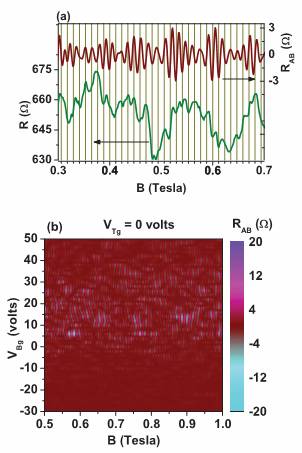
To investigate the Aharonov-Bohm oscillations, we scanned the magnetic field at a ramp rate of 5 mT/min. The magnetoresistance at 250 mK shows a pronounced periodic oscillation on top of a slowly varying aperiodic background. The aperiodic background arises due to conductance fluctuations originating from the penetration of the magnetic field in the arms apdc . Using Fourier analysis, we filtered out the aperiodic conductance fluctuations and obtained the Aharonov-Bohm flux-dependent part of the resistance (). Fig. 2(a) shows magnetoresistance data for = 4 V with zero top gate voltage (the graphene sections in both arms of the interferometer are p-type in this case). A pronounced resistance oscillation is visible in the raw data. The oscillating part of the resistance shows that the period of is about 12 mT. For Aharonov-Bohm oscillation, the observed period corresponds to a ring with a radius of 330 nm which is in reasonable agreement with the radius of our device. At a bias current of 10 nA, the peak-to-peak amplitude of is up to % of the total resistance.
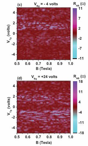
In Fig. 2(b) we show the variation of as a function of magnetic field for various back gate voltages with zero top gate voltage. It is evident that oscillations are observed over the entire range of back gate voltage and magnetic field (also in supporting material, Fig. S3). For a fixed magnetic field, shows oscillatory behavior as a function of gate voltage. In Fig. 2(c) we show as a function of magnetic field for various top gate voltages and a fixed (4 V) back gate voltage. It is important to note that application of the top gate voltage does not destroy the Aharonov-Bohm oscillations: they are clearly visible even when the carrier types in the two arms of the ring are different. Observing the Aharonov-Bohm oscillations clearly demonstrates quantum interference between electron-type states in graphene in one arm and the hole-type states in the other arm. Similar results were obtained for a fixed positive back gate voltage as a function of top gate voltage (Fig. 2(d)). We find pronounced Aharonov-Bohm oscillations for all possible combinations of the carrier types in the two arms: p-p∗, n-n∗, p-n∗ and n-p∗.
We do not observe any higher harmonics (those with periodicity where is an integer) as a function of top gate voltage for any value of the back gate voltage. Also, the nature of the oscillations remains the same at relatively high magnetic field (up to Tesla, the maximum field used in our measurements). This indicates that the main contribution to the Aharonov-Bohm oscillations comes from the direct paths through the arms of the ring ab_2 ; ab_3 . The overall resistance increases with increasing magnetic field and the oscillations survive even at high field, but no significant reduction or increase of the oscillation amplitude was observed as a function of the magnetic field (supporting material, Fig. S4), in contrast to previous observations graphene_1 ; graphene_2 ; graphene_3 . An increase in the oscillation amplitude has been observed previously in graphene nanorings in the high field region graphene_1 , and was suggested to be due to orbital effects graphene_1 ; graphene_2 or scattering on magnetic impurities graphene_2 .
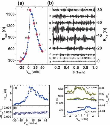
In contrast to the previous work on graphene rings graphene_1 ; graphene_2 ; graphene_3 ; graphene_4 , we find pronounced Aharonov-Bohm oscillations at the Dirac point (shown in Fig. 3(a), 3(b) and supporting material, Fig. S3). The r.m.s. value of the oscillation amplitude () increases as the back gate voltage approaches the Dirac point and becomes maximum at that point (as shown in Fig. 3(b) and (c)). Fig. 3(d) shows , where is the resistance averaged over the entire magnetic field scan for fixed back and top gate voltages, as a function of back gate voltage for zero top gate voltage. It is clear from the data that the value of is mostly independent of the back gate voltage. This indicates that the visibility of remains unaffected by the back gate voltage and shows a linear dependence on (supporting material, Fig. S5) linear_1 ; graphene_1 ; linear_2 . Similar results are obtained as a function of top gate voltage for a fixed back gate voltage (Fig. 3(e)). For a fixed (positive or negative) back gate voltage shows similar behavior, with similar amplitude for both positive and negative top gate voltages. We conclude that the nature and the visibility of the Aharonov-Bohm oscillation remain the same, regardless of whether the carrier types are the same (n-n∗ or p-p∗) or different (n-p∗ or p-n∗) in the two arms of the interferometer.
It has been demonstrated that electron-hole puddles are present at the charge neutrality point and that these puddles contribute to the observed non-zero conductivity at the Dirac point puddle_1 ; puddle_2 ; puddle_3 ; puddle_4 ; puddle_5 . The typical size of the puddles is found to be on the order of 20nm, which is smaller than the gap between the gold electrodes in our samples. Our observation of pronounced Aharonov-Bohm oscillations at the Dirac point shows that the charge transport through these puddles preserves phase coherence. This is also consistent with our observation of phase coherence away from the Dirac point, in the case when the charge carriers are different in the two arms of the interferometer.
Furthermore, the edge of the top gate on some samples (such as the one pictured in Fig. 1.b.) was between the gold electrodes, allowing us to create a pn-junction in one of the arms of the interferometer. Clear AB oscillations were observed in that case as well. The amplitude of the oscillations was slightly asymmetric as a function of the top gate voltage, which might be expected for Klein tunneling in smooth pn junctions Recher_1 ; Schelter .
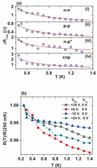
The observation of phase coherence in the interferometer is further supported by the measurements of the temperature dependence of the oscillation amplitude for various back gate and top gate voltages. We found that, irrespective of all possible combinations of the back gate and top gate voltages, shows a dependence (shown in Fig. 4(a)) between 250 mK and 1.4 K. Such temperature dependence of Aharonov-Bohm oscillations has been observed before in various materials, including graphene graphene_1 ; graphene_2 ; temp_2 , and has been attributed to the loss of phase coherence due to thermal averaging temp_2 . With increasing temperature, the sample resistance decreases (Fig. 4(b)) but this change is not significant (%), whereas the decrease in is large (%). The diminishing amplitude of the oscillations reflects the loss of phase coherence with increasing temperature. We found all the features of the samples to be robust and the data were reproducible even after several warm-up and cool-down cycles over months.
Our work represents a clear demonstration of quantum interference between electrons and holes and the efficient transmission of phase information between the electron-type and hole-type regions. These measurements can also give a direct estimate of the lower limit of the phase coherence length at the Dirac point.
References
- (1) Y. Aharonov, and D. Bohm, Phys. Rev. 115, 485 (1959).
- (2) R. Webb, S. Washburn, C. Umbach, and D. C. Laibowitz, Phys. Rev. Lett. 54, 2696 (1985).
- (3) S. Datta et al. Phys. Rev. Lett. 55, 2344 (1985).
- (4) A. Bachtold, et al. Nature 397, 673 (1999).
- (5) B. Lassagne, et al. Phys. Rev. Lett. 98, 176802 (2007).
- (6) H. Peng,et al. Nature Materials 9, 225 (2010).
- (7) K. S. Novoselov, et al. Science 306, 666 (2004).
- (8) K. S. Novoselov, et al. Nature 438, 197 (2005).
- (9) A. K. Geim, and K. S. Novoselov, Nature Mater. 6, 183 (2007).
- (10) M. I. Katsnelson and K. S. Novoselov, Solid State Commun. 143, 3 (2007).
- (11) M. I. Katsnelson, EPL 89, 17001 (2010).
- (12) J. Martin, et al. Nature Physics 4, 144 (2008).
- (13) S. Russo, et al. Phys. Rev. B 77, 085413 (2008).
- (14) M. Huefner, et al. Phys. Status Solidi B 246, 2756 (2009).
- (15) M. Huefner, et al. New Journal of Physics 12, 043054 (2010).
- (16) D. Smirnov, H. Schmidt, and R. J. Haug, Appl. Phys. Lett. 100, 203114 (2012).
- (17) D. A. Bahamon, A. L. C. Pereira, and P. A. Schulz, Phys. Rev. B 79, 125414 (2009).
- (18) D. Gunlycke, D. A. Areshkin, and C. T. White, Appl. Phys. Lett. 90, 142104 (2007).
- (19) Z. Chen, Y.-M. Lin, M. J. Rooks, and P. Avouris, Physica E 40, 228 (2007).
- (20) Y. V. Nazarov, Physica B 189, 57 (1993).
- (21) R. Schuster, et al. Nature 385, 417 (1997).
- (22) A. Oudenaarden, M. H. Devoret, Yu. V. Nazarov, and J. E. Mooij, Nature 391, 768 (1998).
- (23) W. G. van der Wiel, at al. Phys. Rev B 67, 033307 (2003).
- (24) A. Van Oudenaarden, M. H. Devoret, E. H. Visscher, Yu. V. Nazarov, and J. E. Mooij, Phys. Rev. Lett. 78, 3539 (1997).
- (25) L. Angers, et al. Phys. Rev. B 75, 115309 (2007).
- (26) S. Adam, E. H. Hwang, V. M. Galitski, and S. D. Sarma, Proc. Natl. Acad. Sci. U.S.A. 104, 18392 (2007).
- (27) E. H. Hwang, S. Adam, and S. Das Sarma, Phys. Rev. Lett. 98, 186806 (2007).
- (28) V. V. Cheianov, V. I. Fal’ko, B. L. Altschuler, and I. L. Aleiner, Phys. Rev. Lett. 99, 176801 (2007).
- (29) S. Cho, and M. S. Fuhrer, Phys. Rev. B 77, 081402(R) (2008).
- (30) P. Recher, et al. Phys. Rev. B 76, 235404 (2007).
- (31) J. Schelter, P. Recher, B. Trauzettel, Solid State Communications, http://dx.doi.org/10.1016/j.ssc.2012.04.039 (2012).
- (32) S. Washburn, and R. A. Webb, Advances in Physics 35, 375 (1986).