Tight-binding model and direct-gap/indirect-gap transition in single-layer and multi-layer MoS2
Abstract
In this paper we present a paradigmatic tight-binding model for single-layer as well as for multi-layered semiconducting MoS2 and similar transition metal dichalcogenides. We show that the electronic properties of multilayer systems can be reproduced in terms of a tight-binding modelling of the single-layer hopping terms by simply adding the proper interlayer hoppings ruled by the chalcogenide atoms. We show that such tight-binding model permits to understand and control in a natural way the transition between a direct-gap band structure, in single-layer systems, to an indirect gap in multilayer compounds in terms of a momentum/orbital selective interlayer splitting of the relevant valence and conduction bands. The model represents also a suitable playground to investigate in an analytical way strain and finite-size effects.
I Introduction
The isolation of flakes of single-layer and few-layer graphenenovoselov1 ; novoselov2 ; ZK05 has triggered a huge burst of interest on two-dimensional layered materials because of their structural and electronic properties. Due to its huge electronic mobility, graphene has been in the last years the main focus of the research in the field. However, a drawback in engineering graphene-based electronic device is the absence of a gap in the monolayer samples, and the difficulty in opening a gap in multilayer systems without affecting the mobility. As an alternative route, recent research is exploring the idea of multilayered heterostructures built up from interfacing different twodimensional materials.britnell Along this perspective, semiconducting dichalcogenides such as MoS2, MoSe2, WS2, etc. are promising compounds since they can be easily exfoliated and present a suitable small gap both in single-layer and in few-layer samples. Quite interestingly, in few-layer MoS2 the size and the nature of the gap depends on the number of MoS2 layers, with a transition between a direct gap in monolayer () compounds to a smaller indirect gap for . li ; lebegue ; mak ; splendiani In addition, the electronic properties appear to be highly sensitive to the external pressure and strain, which affect the insulating gap and, under particular conditions, can also induce a insulator/metal transition. feng ; lu ; pan ; peelaers ; yun ; scalise1 ; scalise2 ; li3 ; ghorbani ; shi ; hromadova Another intriguing feature of these materials is the strong entanglement between the spin and the orbital/valley degrees of freedom, which permits, for instance, to manipulate spins by means of circularly polarized light.mak12 ; mak13 ; cao ; sallen ; xiao ; wu ; zeng ; OR13 Moreover, in MoSe2, a transition between a direct to an indirect gap was observed as a function of temperature.tongay
On the theoretical level, the description of its low-energy electronic properties is enormously facilitated by the the availability of a paradigmatic Hamiltonian model for the single-layer in terms of few tight-binding (TB) parameterswallace ; reich2002 (actually only one, the nearest neighbors carbon-carbon hopping , in the simplest case).pacoreview The well-known Dirac equation can thus be derived from that as a low-energy expansion. Crucial to the development of the theoretical analysis in graphene is also the fact that model Hamiltonians for multilayer graphenes can be built using the single-layer TB description as a fundamental block and just adding additional interlayer hopping terms.mccann ; nilsson ; pp1 ; pp2 ; abp ; koshino1 ; koshino2 ; koshino3 ; zhang ; yuan ; yan ; olsen ; mak4 ; lui ; bao ; ubrig Different stacking orders can be also easily investigated. The advantage of such tight-binding description with respect to first-principles calculations is that it provides a simple starting point for the further inclusion of many-body electron-electron effects by means of Quantum Field Theory (QFT) techniques, as well as of the dynamical effects of the electron-lattice interaction. Tight-binding approaches can be also more convenient than first-principles methods such as Density Functional Theory (DFT) for investigating systems involving a very large number of atoms. Although DFT methods are currently able to handle systems with hundreds or even thousands of atomssiesta1 ; siesta2 , and have been thoroughly applied to large scale graphene-related problemsfuhrer ; wang ; lehtinen ; novaes , they are still computationally challenging and demanding. Therefore, TB has been the method of choice for the study of disordered and inhomogeneous systemsho ; palacios ; pereira ; carpio ; lopezsancho ; ribeiro ; yuan1 ; yuan2 ; neek ; yuan3 ; leconte2010 ; soriano2011 ; leconte2011 ; vantuan materials nanostructured in large scales (nanoribbons, ripples)zheng ; guinea08 ; castro1 ; castro2 ; castro3 ; castro4 ; cresti ; huang ; klymenko or in twisted multilayer materials.LdS ; mele1 ; mele2 ; shallcross ; morell ; degail ; mac ; morell2 ; moon1 ; moon2 ; sanjose ; tabert
While much of the theoretical work of graphenic materials has been based on tight-binding-like approaches, the electronic properties of single-layer and few-layer dichalcogenides have been so far mainly investigated by means of DFT calculations.li ; lebegue ; splendiani ; feng ; lu ; pan ; peelaers ; yun ; scalise1 ; scalise2 ; li3 ; ghorbani ; shi ; hromadova ; kaasbjerg ; kaasbjerg2 ; feng2 ; kadantsev ; kosmider ; zibouche ; li4 , despite early work in non-orthogonal tight binding models for transition metal dichalcogenides.bromley Few simplified low-energy Hamiltonian models has been presented for these materials, whose validity is however restricted to the specific case of single-layer systems. An effective low-energy model was for instance introduced in Refs. xiao, ; korma, to discuss the spin/orbital/valley coupling at the K point. Being limited to the vicinity of the K point, such model cannot be easily generalized to the multilayer case where the gap is indirect with valence and conduction edges located far from the K point. An effective lattice TB Hamiltonian was on the other hand proposed in Refs. asgari, , valid in principle in the whole Brillouin zone. However, the band structure of the single-layer lacks the characteristic second minimum in the conduction band (see later discussion) that will become the effective conduction edge in multilayer systems, so that also in this case the generalization to the multilayer compounds is doubtful. In addition, the use of an overlap matrix makes the proposed Hamiltonian unsuitable for a straightforward use as a basis for QFT analyses. This is also the case for a recent model proposed in Ref. zahid, , where the large number (ninetysix) of free fitting parameters and the presence of overlap matrix make such model inappropriate for practical use within the context of Quantum Field Theory.
In this paper we present a suitable tight-binding model for the dichalcogenides valid both in the single-layer case and in the multilayer one. Using a Slater-Koster approach,sl and focusing on MoS2 as a representative case, we analyze the orbital character of the electronic states at the relevant high-symmetry points. Within this context we show that the transition from a direct gap to an indirect gap in MoS2 as a function of the number of layers can be understood and reproduced in a natural way as a consequence of a momentum/orbital selective interlayer splitting of the main relevant energy levels. In particular, we show that the orbital of the S atoms plays a pivotal role in such transition and it cannot be neglected in reliable tight-binding models aimed to describe single-layer as well as multi-layer systems. The tight-binding description here introduced can represent thus the paradigmatic model for the analysis of the electronic properties in multilayer systems in terms of intra-layer ligands plus a finite number of interlayer hopping terms. Such tight-binding model, within the context of the Slater-Koster approach, provides also a suitable tool to include in an analytical and intuitive way effects of pressure/strain by means of the modulation of the interatomic distances. The present analysis defines, in addition, the minimum constraints that the model has to fulfill to guarantee a correct description of the band structure of multi-layer compounds.
The paper is structured as follows: in Section II we present DFT calculations for single-layer and multi-layer (bulk) MoS2, which will be here used as a reference for the construction of a tight-binding model. In Section III we describe the minimum tight-binding model for the single-layer case needed to reproduce the fundamental electronic properties and the necessary orbital content. The decomposition of the Hamiltonian in blocks and the specific orbital character at the high-symmetry points is discussed. The extension of the tight-binding model to the bulk case, taken as representative of multilayer compounds, is addressed in Section IV. We pay special attention to reveal the microscopic origin of the change between a direct-gap to indirect-gap band structure. In Section V we summarize the implications of our analysis in the building of a reliable tight-binding model, and we provide a possible set of tight-binding parameters for the single-layer and multilayer case.
II DFT calculations and orbital character
In the construction of a reliable TB model for semiconducting dichalcogenides we will be guided by first-principles DFT calculations taht will provide the reference on which to calibrate the TB model. We will focus here on MoS2 as a representative case, although we have performed first-principle calculations for comparison also on WS2. The differences in the electronic structure and in the orbital character of these two compounds are, however, minimal and they do not involve any different physics. The structure of single-layer and multilayer MoS2 is depicted in Fig. 1.
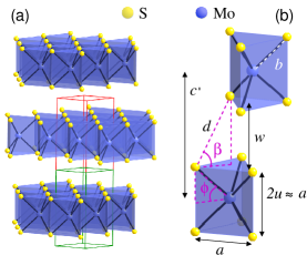
The basic unit block is composed of an inner layer of Mo atoms on a triangular lattice sandwiched between two layers of S atoms lying on the triangular net of alternating hollow sites. Following standard notations,bromley we denote as the distance between nearest neighbor in-plane Mo-Mo and S-S distances, as the nearest neighbor Mo-S distance and as the distance between the Mo and S planes. The MoS2 crystal forms an almost perfect trigonal prism structure with and very close to the their ideal values and . In our DFT calculations, we use experimental values for bulk MoS2,bromley namely Å, Å, and, in bulk systems, a distance between Mo planes as Å, with a lattice constant in the 2H-MoS2 structure of . The in-plane Brillouin zone is thus characterized by the high-symmetry points , K, and M. DFT calculations are done using the Siesta code.siesta1 ; siesta2 We use the exchange-correlation potential of Ceperly-Alderceperley_alder_1980 as parametrized by Perdew and Zunger.perdew We use also a split-valence double- basis set including polarization functions.arsan99 The energy cutoff and the Brillouin zone sampling were chosen to converge the total energy.
The electronic dispersion for the single-layer MoS2 is nowadays well known. We will only focus on the block of bands containing the first four conduction bands and by the first seven valence bands, in an energy window of from -7 to 5 eV around the Fermi level. Our DFT calculations are shown in Fig. 2, where we show the orbital character of each band.
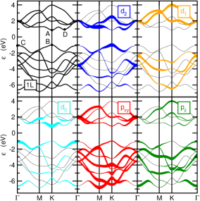
We use here the shorthand notation to denote Mo , orbitals; for the Mo , orbitals; for the Mo orbital; (or simply ) to denote the S , orbitals; and (or simply ) for the S orbital. The four conduction bands and the seven valence bands are mainly constituted by the five 4 orbitals of Mo and the six (three for each layer) 3 orbitals of S, which sum up to the % of the total orbital weight of these bands.
A special role in the electronic properties of these materials is played by the electronic states labeled as (A)-(D) and marked with black bullets in Fig. 2. A detailed analysis of the orbital character of each energy level at the main high-symmetry points of the Brillouin zone, as calculated by DFT, is provided in Table 1.
| energy | main | second | other | sym. | TB |
| DFT (eV) | orb. | orb. | orbs. | label | |
| point | |||||
| 2.0860∗ | 68 % | 29 % | 3 % | E | |
| 1.9432∗ | 58 % | 36 % | 6 % | O | |
| -1.0341 | 66 % | 28 % | 6 % | E | |
| -2.3300∗ | 54 % | 42 % | 4 % | O | |
| -2.6801 | 100 % | - | 0 % | O | |
| -3.4869∗ | 65 % | 32 % | 3 % | E | |
| -6.5967 | 57 % | 23 % | 20 % | E | |
| K point | |||||
| 4.0127 | 60 % | 36 % | 4 % | O | |
| 2.5269 | 65 % | 29 % | 6 % | E | |
| 1.9891 | 50 % | 31 % | 19 % | O | |
| 0.8162 | 82 % | 12 % | 6 % | E | |
| -0.9919 | 76 % | 20 % | 4 % | E | |
| -3.1975 | 67 % | 27 % | 6 % | O | |
| -3.9056 | 85 % | - | 15 % | O | |
| -4.5021 | 65 % | 25 % | 10 % | E | |
| -5.0782 | 71 % | 12 % | 17 % | E | |
| -5.5986 | 66 % | 14 % | 20 % | E | |
| -6.4158 | 60 % | 37 % | 3 % | O | |
∗Double-degenerate level
We can notice that an accurate description of the conduction and valence band edges (A)-(B) at the K point involves at least the Mo orbitals , , , and the S orbitals , . Along this perspective, a 5-band tight-binding model, restricted to the subset of these orbitals, was presented in Ref. asgari, , whereas even the S orbitals were furthermore omitted in Ref. xiao, .
The failure of this latter orbital restriction for a more comprehensive description is however pointed out when analyzing other relevant high-symmetry Brillouin points. In particular, concerning the valence band, we can notice a second maximum at the point, labeled as (C) in Fig. 2, just meV below the real band edge at the K point and with main - orbital character. The relevance of this secondary band extreme is evident in the multilayer compounds (), where such maximum at increases its energy to become the effective band edge. li ; splendiani
The band structure with the orbital character for the bulk () case, representative of the multilayer case, is shown in Fig. 3.
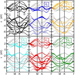
A similar change of the topology of the band edge occurs in the conduction band. Here a secondary minimum, labeled as (D) in Fig. 2, at , midway along the -K cut, is present in the single-layer compounds. Such minimum however moves down in energy in multilayer systems to become the effective conduction band edge.li ; splendiani Even in this case, a relevant component is involved in the orbital character of this electronic state. The topological changes of the location of the band edges in the Brillouin zone are responsible for the observed switch from a direct to an indirect gap in multilayer samples. As we will see, thus, the inclusion of the orbitals in the full tight-binding Hamiltonian is not only desirable for a more complete description, but it is also unavoidable to understand the evolution of the band structure as a function of the number of layers.
III Tight-binding description of the single-layer
The aim of this section is to define a tight-binding model for the single-layer which will be straightforwardly generalizable to the multilayer case by adding the appropriate interlayer hopping. We will show that, to this purpose, all the Mo orbitals and the S orbitals are needed to be taken into account. Considering that the unit cell contains two S atoms, we define the Hilbert space by means of the 11-fold vector:
| (1) |
where creates an electron in the orbital of the Mo atom in the -unit cell, creates an electron in the orbital of the top () layer atom S in the -unit cell, and creates an electron in the orbital of the bottom () layer atom S in the -unit cell.
Once the Hilbert space has been introduced, the tight-binding model is defined by the hopping integrals between the different orbitals, described, in the framework of a Slater-Koster description, in terms of , and ligands.sl In order to provide a tight-binding model as a suitable basis for the inclusion of many-body effects by means of diagrammatic techniques, we assume that the basis orbitals are orthonormal, so that the overlap matrix is the unit matrix. A preliminary analysis based on the interatomic distance can be useful to identify the most relevant hopping processes. In particular, these are expected to be the ones between nearest neighbor Mo-S (interatomic distances Å) and between the nearest neighbor in-plane Mo-Mo and between the nearest neighbor in-plane and out-of-plane S-S atoms (interatomic distance Å). Further distant atomic bonds, in single-layer systems, start from hopping between second nearest neighbor Mo-S atoms, with interatomic distance Å, and they will be here discarded.
All the hopping processes of the relevant pair of neighbors are described in terms of the Slater-Koster parameters, respectively , (Mo-S bonds), , , (Mo-Mo bonds), and , (S-S bonds). Additional relevant parameters are the crystal fields , , , , , describing respectively the atomic level the (), the (, ), the (, ) Mo orbitals, the in-plane (, ) S orbitals and of the out-of-plane S orbitals. We end up with a total of 12 tight-binding parameters to be determined, namely: , , , , , , , , , , , .
In the orbital basis of Eq. (1), we can write thus the tight-binding Hamiltonian in the form:
| (2) |
where is the Fourier transform of in momentum space. The Hamiltonian matrix can be written (we drop for simplicity from now on the index ) as:
| (6) |
where describes the in-plane hopping in the top and bottom S layer, namely,
| (10) |
the in-plane hopping in the middle Mo layer, namely,
| (16) |
the vertical hopping between S orbitals in the top and bottom layer,
| (20) |
and , the hopping between Mo and S atoms in the top and bottom planes, respectively:
| (26) |
| (32) |
Here and in the following, for the sake of compactness, we use the shorthand notation and . An explicit expression for the different Hamiltonian matrix elements in terms of the Slater-Koster tight-binding parameters can be provided following the seminal work by Doran et al. (Ref. doran, ) and it is reported for completeness in Appendix A.
Eqs. (2)-(32) define our tight-binding model in terms of a Hamiltonian which can be now explicitly solved to get eigenvalues and eigenvectors in the whole Brillouin zone or along the main axes of high symmetry. It is now an appealing task to associate each DFT energy level with the Hamiltonian eigenvalues, whose eigenvectors will shed light on the properties of the electronic states. Along this line, we are facilitated by symmetry arguments which permit, in the monolayer compounds, to decoupled the Hamiltonian in Eq. (6), in two main blocks, with different symmetry with respect to the mirror inversion .doran This task is accomplished by introducing a symmetric and antisymmetric linear combination of the orbital of the S atoms on the top/bottom layers. More explicitly, we use the basis vector
| (33) |
where , . Note that our basis differs slightly with respect to the one employed in Ref. doran, because we have introduced explicitly the proper normalization factors to make it unitary. In this basis we can write thus
| (36) |
where is a block with even (E) symmetry with respect to the mirror inversion , and a block with odd (O) symmetry. We should remark however that such decoupling holds true only in the single-layer case and only in the absence of a -axis electric field, as it can be induced by substrates or under gating conditions. In the construction of a tight-binding model that could permit a direct generalization to the multilayer case, the interaction between the band blocks with even and odd symmetry should be thus explicitly retained.
The association between DFT energy levels and tight-binding eigenstates is now further simplified on specific high-symmetry points of the Brillouin zone. Most important are the and the points, which are strictly associated with the direct and indirect gap in monolayer and multilayered compounds.
III.1 point
We present here a detailed analysis of the eigenstates and their orbital character at the point. For the sake of simplicity, we discuss separately the blocks with even and odd symmetry with respect to the inversion . The identification of the DFT levels with the tight-binding eigenstates is facilitated by the possibility of decomposing the full Hamiltonian in smaller blocks, with typical size (dimers) or (monomers). In particular, the block with even symmetry can be decomposed (see Appendix B for details) as:
| (40) |
Here each matrix, , represents a block where the indices describe the orbital character of the dimer. In particular, involves only Mo-orbitals and S-orbitals, whereas involves only the Mo-orbital and the S-orbital. As it is evident in (40), the block appears twice and it is thus double degenerate. Similarly, we have
| (44) |
where the doubly degenerate block involves only Mo-orbitals and S-orbitals, while is a block (monomer) with pure character .
It is also interesting to give a closer look at the inner structure of a generic Hamiltonian sub-block. Considering for instance as an example, we can write
| (47) |
where is an energy level with pure Mo orbital character and an energy level with pure S orbital character. The off-diagonal term acts thus here as a “hybridization”, mixing the pure orbital character of and . The suffix “E” here reminds that the level belongs to the even symmetry block, and it is useful to distinguish this state from a similar one with odd symmetry (and different energy). Keeping as an example, the eigenvalues of a generic block can be obtained analytically:
| (48) |
The explicit expressions of and
in terms of the Slater-Koster tight-binding parameters is reported
in Appendix A.
It is interesting to note that the diagonal
terms () are purely determined
by the crystal fields and by the tight-binding
parameters , , ,
, , connecting Mo-Mo and S-S atoms, whereas
the hybridization off-diagonal terms
depend exclusively on the Mo-S nearest neighbor hopping
,
.
A careful comparison between the orbital character of each eigenvector with the DFT results permits now to identify in an unambiguous way each DFT energy level with its analytical tight-binding counterpart. Such association is reported in Table 1, where also the even/odd symmetry inversion is considered.
The use of the present analysis to characterize the properties of the multilayer MoS2 will be discussed in Section IV.
III.2 K point
A crucial role in the properties of semiconducting dichalcogenides is played by the K point in the Brillouin zone, where the direct semiconducting gap occurs in the single-layer systems. The detailed analysis of the electronic spectrum is also favored here by the possibility of reducing the full Hamiltonian in smaller sub-blocks. This feature is, however, less evident than at the point. The even and odd components of the Hamiltonian take the form:
| (55) |
| (61) |
As for the point, also here the upper labels (E, O) in (E, O) express the symmetry of the state corresponding to the energy level with respect to the inversion. The electronic properties of the Hamiltonian at the K point look more transparent by introducing a different “chiral” base:
| (62) |
where , , , , , , , .
In this basis, the Hamiltonian matrix can be also divided in smaller sub-blocks (see Appendix B) as:
| (66) |
and
| (70) |
As it is evident from the labels, each sub-block is also here a dimer, apart from the term which is a block (monomer) with pure character. The association between the DFT energy levels and the tight-binding eigenstates is reported also for the K point in Table 1.
III.3 Q point
As discussed above, another special point determining the electronic properties of MoS2 is the Q point, halfway between the and K points in the Brillouin zone, where the conduction band, in the single-layer system, has a secondary minimum in addition to the absolute one at the K point. Unfortunately, not being a point of high-symmetry, the tight-binding Hamiltonian cannot be decomposed in this case in simpler smaller blocks. Each energy eigenvalue will contain thus a finite component of all the Mo and S orbitals. In particular, focusing on the secondary minimum in Q, DFT calculations give 46 % , 24 % , 11 % and 9 % . The orbital content of this level will play a crucial role in determining the band structure of multilayer compounds.
III.4 Orbital constraints for a tight-binding model
After having investigated in detail the orbital contents of each eigenstate at the high-symmetry points, and having identified them with the corresponding DFT energy levels, we can now employ such analysis to assess the basilar conditions that a tight-binding model must fulfill and to elucidate the physical consequences.
A first interesting issue is about the minimum number of orbitals needed to be taken into account in a tight-binding model for a robust description of the electronic properties of these materials. A proper answer to such issue is, of course, different if referred to single-layer or multilayer compounds. For the moment we will focus only on the single-layer case but we will underline on the way the relevant features that will be needed to take into account in multi-layer systems.
In single-layer case, focusing only on the band edges determined by the states (A) and (B) at the K point, we can identify them with the eigenstates , , respectively, with a dominant Mo character and a marginal S component, as we show below. It is thus tempting to define a reduced 3-band tight-binding model, keeping only the Mo , , orbitals with dominant character and disregarding the S , orbitals, with a small marginal weight. A similar phenomenological model was proposed in Ref. xiao, . However, the full microscopic description here exposed permits to point out the inconsistency of such a model. This can be shown by looking at Eq. (66). The band gap at K in the full tight-binding model including S , orbitals is determined by the upper eigenstate of ,
| (71) | |||||
and the upper eigenstate of ,
| (72) | |||||
both with main Mo character, while the eigenstate
| (73) | |||||
also with dominant Mo character, but belonging to the block , lies at higher energy (see table 1). The 3-band model retaining only the , orbitals is equivalent to switch off the hybridization terms , , , ruled by , , so that , . In this context the level becomes degenerate with . This degeneracy is not accidental but it reflects the fact that the elementary excitations of the states, in this simplified model, are described by a Dirac spectrum, as sketched in Fig. 4. As a consequence, no direct gap can be possibly established in this framework.

It is worth to mention that a spin-orbit coupling can certainly split the Dirac cone to produce a direct gap at the K point, but it would not explain in any case the direct gap observed in the DFT calculations without spin-orbit coupling.
We should also mention that, in the same reduced 3-band model keeping only the and Mo orbitals, the secondary maximum (C) of the valence band would have a pure orbital character. As we are going to see in the discussion concerning the multilayer samples, this would have important consequences on the construction of a proper tight-binding model.
A final consideration concerns the orbital character of the valence band edge, . This state is associated with the third block of (66) and it results from the hybridization of the chiral state of the Mo orbitals with the chiral state of the S orbitals. The role of the chirality associated with the orbitals, in the presence of a finite spin-orbit coupling, has been discussed in detail in relation with spin/valley selective probes.mak12 ; mak13 ; cao ; sallen ; xiao ; wu ; zeng What results from a careful tight-binding description is that such -orbital chirality is indeed entangled with a corresponding chirality associated with the S orbitals. The possibility of such entanglement, dictated by group theory, was pointed out in Ref. OR13, .
A similar feature is found for the conduction band edge, . So far, this state has been assumed to be mainly characterized by the , and hence without an orbital moment. However, as we can see, this is true only for the Mo part, whereas the S component does contain a finite chiral moment. On the other hand, the spin-orbit associated with the S atoms as well as with other chalcogenides (ex.: Se) is quite small, and taking into account also the small orbital S weight, the possibility of a direct probe of such orbital moment is still to be explored.
IV Bulk system
In the previous section we have examined in detail the content of the orbital character in the main high-symmetry points of the Brillouin zone of the single-layer MoS2, to provide theoretical constraints on the construction of a suitable tight-binding model. Focusing on the low-energy excitations close to the direct gap at the K point, we have seen that a proper model must take into account at least the three Mo orbitals , , and the two S orbitals , . On the other hand, our wider aim is to introduce a tight-binding model for the single-layer that would be the basilar ingredient for a tight-binding model in multilayer systems, simply adding the interlayer coupling.
For the sake of simplicity we focus here on the bulk 2H-MoS2 structure as a representative case that contains already all the ingredients of the physics of multilayer compounds. The band structure for the bulk compound is shown in Fig. 3. As it is known, the secondary maximum (C) of valence band at the point is shifted to higher energies in multilayer systems with respect to the single-layer case, becoming the valence band maximum. At the same time also the secondary minimum (D) of the conduction band, roughly at the Q point, is lowered in energy, becoming the conduction band minimum. All these changes result in a transition between a direct gap material in single-layer compounds to indirect gap systems in the multilayer case. Although such intriguing feature has been discussed extensively and experimentally observed, the underlying mechanism has not been so far elucidated. We will show here that such topological transition of the band edges can be naturally explained within the context of a tight-binding model as a result of an orbital selective (and hence momentum dependent) band splitting induced by the interlayer hopping.
The orbital content of the bulk band structure along the same high-symmetry lines as in the single-layer case is shown in Fig. 3. We will focus first on the K point, where the single-layer system has a direct gap. We note that the direct gap at K is hardly affected. The interlayer coupling produces just a very tiny splitting of the valence band edge , while the conduction band edge at K becomes doubly degenerate.
Things are radically different at the point. The analysis of the orbital weight in Fig. 3 shows indeed that there is a sizable splitting of the level, of the order of eV. A bit more difficult to discern, because of the multi-orbital component, but still visible, is the splitting of the secondary minimum (D) of the conduction band in Q. This is clearest detected by looking in Fig. 3 at the and characters, which belong unically to the E block. One can thus estimate from DFT a splitting of this level at the Q point of eV.
We are now going to see that all these features are consistent with a tight-binding construction where the interlayer hopping acts as an additional parameter with respect to the single-layer tight-binding model. From the tight-binding point of view, it is clear that the main processes to be included are the interlayer hoppings between the external S planes of each MoS2 block. This shows once more the importance of including the S orbital in a reliable tight-binding model. Moreover, for geometric reasons, one could expect that the interlayer hopping between the orbitals, pointing directly out-of-plane, would be dominant with respect to the interlayer hopping between , . This qualitative argument is supported by the DFT results, which indeed report a big splitting of the level at the point, with a 27 % of component, but almost no splitting of the degenerate at eV, with 68 % component of , .
We can quantify this situation within the tight-binding description by including explicitly the interlayer hopping between the -orbitals of the S atoms in the outer planes of each MoS2 layer, with interatomic distance Å (see Fig. 1). These processes will be parametrized in terms of the interlayer Slater-Koster ligands , . The Hilbert space is now determined by a 22-fold vector, defined as:
| (74) |
where represents the basis (33) for the layer 1, and the same quantity for the layer 2. The corresponding Hamiltonian, in the absence of interlayer hopping, would read thus:
| (77) |
where , refer to the intralayer Hamiltonian for the layer 1 and 2, respectively.
Note that the Hamiltonian of layer 2 in the 2H-MoS2 structure is different with respect to the one of layer 1. From a direct inspection we can see that the elements of layer 2 are related to the corresponding elements of layer 1 as:
| (78) |
where , , and if the orbital has even symmetry for , and if it has odd symmetry. We note that both effects can be re-adsorbed in a different redefinition of the orbital basis so that the eigenvalues of are of course the same as the eigenvalues of .
Taking into account the inter-layer S-S hopping terms, we can write thus:
| (81) |
where is here the interlayer hopping Hamiltonian, namely:
| (84) |
where and
| (87) |
| (90) |
| (93) |
| (97) |
The analytical expression of the elements as functions of the Slater-Koster interlayer parameters , is provided in Appendix A. Note that, in the presence of interlayer hopping in the bulk MoS2, we cannot divide anymore, for generic momentum , the Hamiltonian in smaller blocks with even and odd symmetry with respect to the change . The analysis is however simplified at specific high-symmetry points of the Brillouin zone. In particular, for (), we can easily see from (84) that the block () with even symmetry and the block () with odd symmetry are still decoupled.
Exploiting this feature, we can now give a closer look at the high-symmetry points.
IV.1 point
In Section III we have seen that at the point the Hamiltonian can be decomposed in blocks. Particularly important here is the block whose upper eigenvalue , with main orbital character and a small component, represents the secondary maximum (C) of the valence band. A first important property to be stressed in bulk systems is that, within this (Mo )+(S ) tight-binding model, the interlayer coupling at the point does not mix any additional orbital character. This can be seen by noticing that the interlayer matrix is diagonal at the point. Focusing on the levels, we can write thus a reduced Hamiltonian (see Appendix B):
| (102) |
where represents the interlayer hopping mediated by , between orbitals belonging to the outer S planes on different layers. Eq. (102) is important because it shows that the qualitative idea that each energy level in the bulk system is just split by the interlayer hopping is well grounded. In particular, under the reasonable hypothesis that the interlayer hopping is much smaller than intralayer processes, denoting , the two eigenvalues with primary components, we get:
| (103) | |||||
A similar situation is found for the other blocks , , and the block . Most important, tracking the DFT levels by means of their orbital content, we can note that both levels and undergo a quite large splitting eV, and the level a splitting eV, whereas the levels , are almost unsplit. This observation strongly suggest that, as expected, the interlayer hopping between , orbitals is much less effective than the interlayer hopping between .
Similar conclusion can be drawn from the investigation of the energy levels at the K point, although the analysis is a bit more involved.
IV.2 K point
The properties of the bulk system at the K point are dictated by the structure of the interlayer matrix which, in the basis defined in Eq. (74), at the K point reads:
| (107) |
As discussed in detail in Appendix B, the electronic structure is made more transparent by using an appropriate chiral basis, which is a direct generalization of the one for the single-layer. We can thus write the even and odd parts of the resulting Hamiltonian in the form:
| (111) | |||||
| (115) |
where
| (120) | |||||
| (125) | |||||
| (129) | |||||
| (134) |
We can notice that Eq. (125) has the same structure as (102), with two degenerate sub-blocks hybridized by a non-diagonal element ( in this case). This results in a splitting of the single-layer levels , . The two levels , , by looking at their orbital character, can be identified in DFT results in the small splitting of the (B) level, confirming once more the smallness of the interlayer - hopping.
Less straightforward is the case of the block where the hybridization term mixes two different sub-blocks, and . In this case, a mixing of the orbital character will result. We note, however, that the block appears twice in (111), so that each energy level will result double-degenerate, in particular the minimum (A) of the conduction band at K. Note, however, that the negligible shift of such energy level in the DFT calculations with respect to the single-layer case is an indication that also the interlayer hopping element , between on one layer and , on the other one, is negligible.
IV.3 Q point
An analytical insight on the electronic structure at the Q point was not available in single-layer systems and it would be thus even more complicate in the bulk case. A few important considerations, concerning the minimum (D), can be however drawn from the DFT results. In particular, we note that in the single-layer case this energy level had a non-vanishing component. As we have seen above, the interlayer hopping between orbitals appears to be dominant with respect to the interlayer hopping between and and with respect to the mixed interlayer hopping -. We can thus expect a finite sizable splitting of the (D) level, containing a finite component, with respect to the negligible energy shift of (A), which depends on the mixed interlayer process .
V Momentum/orbital selective splitting and comparison with DFT data
In the previous section we have elucidated, using a tight-binding model, the orbital character of the band structure of MoS2 on the main high-symmetry points of the Brillouin zone. We have shown how a reliable minimal model for the single-layer case needs to take into account at least the , orbitals of the S atoms in addition to the orbitals of Mo. A careful inspection of the electronic structure shows also that the band edges at the K point defining the direct band gap in the single-layer case are characterized not only by a chiral order of the Mo orbitals, as experimentally observed, but also by an entangled chiral order of the minor component of the S orbitals.
An important role is also played by the orbitals of the S atoms. In single-layer systems, the orbital character is particularly relevant in the (C) state, characterizing a secondary maximum in the valence band at the point, and in the (D) state, which instead provides a secondary minimum in the conduction band at the Q point.
The component becomes crucial in multilayer compounds where a comparison with DFT results shows that the interlayer coupling is mainly driven by the - hopping whereas - - are negligible. This results in an orbital-selective and momentum-dependent interlayer splitting of the energy levels, being larger for the (C) and (D) states and negligible for (A) and (B). This splitting is thus the fundamental mechanism responsible for the transition from a direct (A)-(B) gap in single-layer compounds to an indirect (C)-(D) gap in multilayer systems. Controlling these processes is therefore of the highest importance for electronic applications. Note that such direct/indirect gap switch is discussed here in terms of the number of layers. On the other hand, the microscopical identification of such mechanism, which is essentially driven by the interlayer coupling, permits to understand on the physical ground the high sensitivity to pressure/strain effects, as well as to the temperature, via the lattice expansion.
Finally, in order to show at a quantitative level how the orbital content determines the evolution of the electronic structure from single-layer to multilayer compounds, we have performed a fitting procedure to determine the tight-binding parameters that best reproduce the DFT bands within the model defined here. The task was divided in two steps: ) we first focus on the single-layer case to determine the relevant Slater-Koster intra-layer parameters in this case; ) afterwards, keeping fixed the intralayer parameters, we determine the interlayer parameters. To this purpose we employ a simplex methodnumrecipes to minimize a weighted mean square error between the TB and DFT band energies, defined as
| (135) |
where is the dispersion on the -th band of the 11 band block under consideration, the corresponding tight-binding description, and a band/momentum resolved weight which can be used to improve fitting over particular -regions or over selected bands. In spite of many efforts, we could not find a reliable fit for the whole electronic structure including the seven valence bands and the four lowest conduction bands.noteTB As our analysis and our main objective concerns the description of the valence and conduction bands that define the band gap of these systems, we focus on finding a set of parameters that describe properly these bands. Since both the lowest conduction and highest valence band belong to the electronic states with even symmetry, the fit was performed in the orbital space defined by this symmetry. In addition, due to the degeneracy at the point and to the band crossing along the -M direction, the two conduction bands with even symmetry for were considered in the fit. Additionally, we give a larger weight to the (A)-(D) band edges in order to obtain a better description of the most important features of the band structure.
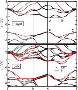
Our best fit for the single-layer case is shown in the top panel of Fig. 5 (where only the TB bands with even symmetry are shown), compared with the DFT bands, and the corresponding tight-binding parameters are listed in Table 2.
| Crystal Fields | -1.016 | |||
| – | ||||
| -2.529 | ||||
| -0.780 | ||||
| -7.740 | ||||
| Intralayer Mo-S | -2.619 | |||
| -1.396 | ||||
| Intralayer Mo-Mo | -0.933 | |||
| -0.478 | ||||
| -0.442 | ||||
| Intralayer S-S | 0.696 | |||
| 0.278 | ||||
| Interlayer S-S | -0.774 | |||
| 0.123 |
Note that, due to the restriction of our fitting procedure to only some bands belonging to the block with even symmetry, the atomic crystal field for the Mo orbitals , (not involved in the fitting procedure) results undetermined. The fit reported in Fig. 5 agrees in a qualitative way with the DFT results, showing, in particular, a direct gap at the K point [(A) and (B) band edges] and secondary band edges for the valence and conduction bands lying at the (C) and the Q point (D), respectively.
Turning now to the bulk system, the further step of determining the interlayer hopping parameters , , is facilitated by the strong indication, from the DFT analysis, of a dominant role of the interlayer hopping between the orbitals and a negligible role of the interlayer hopping between the orbitals. Focusing on the point, these two different hopping processes are parametrized in terms of the corresponding interlayer parameters and , as discussed in Appendix B. We can thus approximate , providing a constraint between and , and leaving thus only one effective independent fitting parameter: . We determine it, and hence and , by fixing the effective splitting of the level as in the DFT data. The values of and found in this way are also reported in Table 2, and the resulting band structure in the lower panel of Fig. 5, where only the TB bands with even symmetry are shown. We stress that the intralayer hoppings are here taken from the fitting of the single-layer case. The agreement between the DFT and the tight-binding bands is also qualitatively good in this case. In particular, we would like to stress the momentum/orbital selective interlayer splitting of the bands, which is mainly concentrated at the point for the valence band and at the Q point for the conduction band. This yields to the crucial transition between a direct gap in single-layer MoS2, located at the K point, to an indirect gap -Q in multilayer systems.
On more quantitative grounds, we can see that, while the interlayer splitting of the condution level is easily reproduced, the corresponding splitting of the conduction band at the Q point is somewhat underestimated in the tight-binding model ( eV) as compared to the DFT data ( eV). This slight discrepancy is probably due to the underestimation, in the tight-binding model, of the character of the conduction band at the Q point. As a matter of fact, the set of TB parameters reported in Table 2 gives at the Q point of the conduction band, for the single-layer case, only a 3.8% of orbital character, in comparison with the 11% found by the DFT calculations. It should be kept in mind, however, that the optimization of the tight-binding fitting parameters in such a large phase space (12 free parameters) is a quite complex and not univocal procedure, and other solutions are possible. In particular, a simple algebric analysis suggests that an alternative solution predicting 11% of character at the Q point would yield to a corresponding splitting of the order of eV, in quantitative agreement with the DFT data. A more refined numerical search in the optimization of the tight-binding parameters, using global minimization techniques, might result in better comparison with the DFT results and further work along this line should be of great interest.
VI Conclusions
In this paper we have provided an analytic and reliable description of the electronic properties of single-layer and multi-layer semiconduting transition-metal dichalcogenides in terms of a suitable tight-binding model. We have shown that the band structure of the multilayer compounds can be generated from the tight-binding model for the single-layer system by adding the few relevant interlayer hopping terms. The microscopic mechanism for the transition between a direct-gap to an indirect-gap from single-layer to multi-layer compounds is thus explained in terms of a momentum/orbital selective interlayer band splitting, where the orbital component of the S atoms plays a central role. The present work provides with a suitable basis for the inclusion of many-body effects within the context of Quantum Field Theory and for the analysis of local strain effects related to the modulation of the Mo-S, Mo-Mo and S-S ligands.
Acknowledgements.
F.G. acknowledges financial support from MINECO, Spain, through grant FIS2011-23713, and the European Union, through grant 290846. R. R. acknowledges financial support from the Juan de la Cierva Program (MINECO, Spain). E.C. acknowledge support from the European FP7 Marie Curie project PIEF-GA-2009-251904. J.A.S.-G. and P.O. ackowledge support from Spanish MINECO (Grants No. FIS2009-12721-C04-01, No. FIS2012-37549-C05-02, and No. CSD2007-00050). J.A.S.-G. was supported by an FPI Fellowship from MINECO.Appendix A Tight-binding Hamiltonian elements
In this Appendix we provide an analyical expression, in terms of the Slater-Koster parameters, for the several intra-layer and inter-layer matrix elements that appear in the Hamiltonian of the tight-binding model. Following Ref. doran, , it is convenient to introduce few quantities that account for the moment dispersion within the Brillouin zone, as functions of the reduced momentum variables , .
We define thus:
| (136) | |||||
| (137) | |||||
| (138) | |||||
| (139) | |||||
| (140) | |||||
| (141) | |||||
| (142) |
A.1 Intra-layer hopping terms
Following Ref. doran, , the intralayer hopping terms appearing in Eqs. (10)-(32) can be written as:
where
| (143) | |||||
| (144) | |||||
| (145) | |||||
| (146) | |||||
| (147) | |||||
| (148) | |||||
| (149) | |||||
| (150) | |||||
| (151) | |||||
| (152) | |||||
| (153) | |||||
| (154) | |||||
| (155) | |||||
| (156) | |||||
| (157) | |||||
| (158) |
Here the angle characterize the structure of the unit cell of the compound and it is determined by purely geometric reasons (see Fig. 1).. For the ideal trigonal prism structure, neglecting the marginal deviations from it in real systems, we have , so that and .
With these expressions, taking into account also the further changes of basis, the Hamiltonian at the point can be divided in sub-blocks as:
| (162) |
| (166) |
where
| (169) |
| (172) |
| (175) |
The parameters can be viewed as “molecular” energy levels, and the quantities as hybridization parameters. Their explicit expressions read:
| (176) | |||||
| (177) | |||||
| (178) | |||||
| (179) | |||||
| (180) | |||||
| (181) | |||||
| (182) | |||||
| (183) | |||||
| (184) | |||||
| (185) | |||||
| (186) | |||||
| (187) | |||||
At the K point, in the proper basis described in the main text, we can write the even and odd blocks of the Hamiltonian as:
| (191) | |||||
| (195) |
where
| (198) |
| (201) |
| (204) |
| (207) |
| (210) |
The parameters , read here:
| (211) | |||||
| (212) | |||||
| (213) | |||||
| (214) | |||||
| (215) | |||||
| (216) | |||||
| (217) | |||||
| (218) | |||||
| (219) | |||||
| (220) | |||||
| (221) | |||||
| (222) | |||||
| (223) | |||||
| (224) | |||||
A.2 Inter-layer hopping terms
Inter-layer hopping is ruled by the Slater-Koster parameters , describing hopping between S- orbitals belonging to different layers.
In terms of the reduced momentum variables , , we have thus:
| (225) | |||||
| (226) | |||||
| (227) | |||||
| (228) | |||||
| (229) | |||||
| (230) | |||||
| (231) |
where
| (232) | |||||
| (233) | |||||
| (234) | |||||
| (235) |
Here is the angle between the line connecting the two S atoms with respect to the S planes (see Fig. 1). Denoting the distance between the two S-planes, we have:
| (236) | |||||
| (237) |
Using typical values for bulk MoS2, Å, and Å, we get and .
At the high-symmetry points , K, we have thus:
| (238) | |||||
| (239) | |||||
| (240) | |||||
| (241) | |||||
Appendix B Decomposition of the Hamiltonian in sub-blocks at high-symmetry points
In this Appenddix we summarize the different unitary transformations that permit to decomposed at special high-symmetry points the higher rank Hamiltonian matrix in smaller sub-locks. In all the cases we treat in a separate way the “even” and “odd” blocks, namely electronix states with even and odd symmetry with respect to the inversion.
B.1 Single-layer
B.1.1 point
In the Hilbert space defined by the vector basis in Eq. (33), the even and odd blocks of the Hamiltonian can be written respectively as:
| (248) |
and
| (254) |
B.1.2 K point
In the basis defined by the Hilbert vector , the Hamiltonian at the K point reads, for the even and odd blocks, respectively:
| (277) |
| (283) |
In order to decopled the Hamiltoniam, it is convenient to introduce the chiral basis defined by the vector in (62). In this Hilbert space we have thus:
| (287) | |||||
| (291) |
where
| (294) | |||||
| (297) | |||||
| (300) | |||||
| (303) | |||||
| (306) |
B.2 Bulk system
The general structure of the tight-binding Hamiltonian for the bulk system, using the basis defined in (74), is provided in Eqs. (81)-(97), where we also remind the symmetry property (78) that related the matrix elements of to .
As mentioned in the main text, for the band structure can be still divided in two independent blocks with even and odd symmetry with respect to the transformation .doran Further simplicication are encountered at the high-symmetry points and K.
B.2.1 point
We first notice that at the point the relation (78) does not play any role, i.e. , where is defined by Eqs. (36)-(44) in the main text.
The Hamiltonian is thus completely determined by the interlayer hopping matrix that at the point reads:
| (310) |
A convenient basis to decoupled the Hamiltonian in smaller subblocks is thus:
| (311) |
where
| (312) | |||||
| (313) | |||||
| (314) | |||||
| (315) | |||||
| (316) | |||||
| (317) |
The resulting total Hamiltonian can be written as:
| (320) |
where
| (324) | |||||
| (328) |
and where
| (333) | |||||
| (338) | |||||
| (343) | |||||
| (346) |
B.2.2 K point
The treatment of the bulk Hamiltonian at the K point, in order to get a matrix clearly divided in blocks, is a bit less straighforward than at the point.
We first notice that the interlayer matrix, in the basis , reads:
| (350) |
We then ridefine the orbitals , (A,S), in order to get, according with (78), .
Following what done for the single layer, we can also introduce here a chiral basis. After a further rearrangement of the vector elements, we define thus the convenient Hilbert space as:
| (351) |
where
| (352) | |||||
| (353) | |||||
| (354) | |||||
| (355) | |||||
| (356) | |||||
| (357) |
References
- (1) K.S. Novoselov, A.K. Geim, S.V. Morozov, D. Jiang, Y. Zhang, S.V. Dubonos, I.V. Gregorieva, and A.A. Firsov, Science 306, 666 (2004).
- (2) K.S. Novoselov, D. Jiang, F. Schedin, T.J. Booth, V.V. Khotkivich, S.V. Morozov, and A.K. Geim, Proc. Nat. Ac. Sc. 102, 10451 (2005).
- (3) Zhang, Yuanbo and Tan, Yan-Wen and Stormer, Horst L and Kim, Philip Nature 438, 201 (2005).
- (4) L. Britnell, R.V. Gorbachev, R. Jalil, B.D. Belle, F. Schedin, A. Mishchenko, T. Georgiou, M.I. Katsnelson, L. Eaves, S.V. Morozov, N.M.R. Peres, J. Leist, A.K. Geim, K. S. Novoselov, and L. A. Ponomarenko, Science 335, 947 (2012).
- (5) T. Li and G. Galli, J. Phys. Chem. 111, 16192 (2007)
- (6) S. Lebègue and O. Eriksson, Phys. Rev. B 79, 115409 (2009).
- (7) K.F. Mak, C. Lee, J. Hone, J. Shan, and T.F. Heinz, Phys. Rev. Lett. 105, 136805 (2010).
- (8) A. Splendiani, L. Sun, Y. Zhang, T. Li, J. Kim, C.-Y. Chim, G. Galli, and F. Wang, Nano Lett. 10, 1271 (2010).
- (9) J. Feng, X. Qian, C.-W. Huang, and J. Li, Nature Photon. 6, 866 (2012).
- (10) P. Lu, X. Wu, W. Guo, and X.C. Zeng, Phys. Chem. Chem. Phys. 14, 13035 (2012).
- (11) H. Pan and Y.-W. Zhang, J. Phys. Chem. C 116, 11752 (2012).
- (12) H. Peelaers and C.G. van de Walle, Phys. Rev. B 86, 241401 (2012).
- (13) W.S. Yun, S.W. Han, S.C. Hong, I.G. Kim, and J.D. Lee, Phys. Rev. B 85, 033305 (2012).
- (14) E. Scalise, M. Houssa, G. Pourtois, V. Afanas’ev, and A. Stesmans, Nano Res. 5, 43 (2012).
- (15) E. Scalise, M. Houssa, G. Pourtois, V. Afanas’ev, and A. Stesmans, Physica E (in press, 2013).
- (16) Y. Li, Y.-l. Li, C.M. Araujo, W. Luo, and R. Ahuja, arXiv:1211.4052 (2012).
- (17) M. Ghorbani-Asl, S. Borini, A. Kuc, and T. Heine, arXiv:1301.3469 (2013).
- (18) H. Shi, H. Pan, Y.-W. Zhang, and B.I. Yakobson, arXiv:1211.5653 (2012).
- (19) L. Hromodová, R. Martoňák, and E. Tosatti, arXiv:1301.0781 (2013).
- (20) K.F. Mak, K. He, J. Shan, and T.F. Heinz, Nature Nanotech. 7, 494 (2012).
- (21) K.F. Mak, K. He, C. Lee, G.H. Lee, J. Hone, T.F. Heinz, and J. Shan, Nature Mat. 12, 207 (2013).
- (22) T. Cao, J. Feng, J. Shi, Q. Niu, and E. Wang, Nature Commun. 3, 887 (2012).
- (23) G. Sallen, L. Bouet, X. Marie, G. Wang, C.R. Zhu, W.P.Han, Y. Lu, P.H. Tan, T. Amand, B.L. Liu, and B. Urbaszek, Phys. Rev. B 86, 081301 (2012).
- (24) D. Xiao, G.-B. Liu, W. Feng, X. Xu, and W. Yao, Phys. Rev. Lett. 108, 196802 (2012).
- (25) S. Wu, J.S. Ross, G.-B. Liu, G. Aivazian, A. Jones, Z. Fei, W. Zhu, D. Xiao, W. Yao, D. Cobden, and X. Xu, Nature Phys. 9, 149 (2013).
- (26) H. Zheng, J. Dai, W. Yao, D. Xiao, and X. Cui, Nature Nanotechn. 7, 490 (2012).
- (27) H. Ochoa and R. Roldán, arXiv:1303.5860 (2013).
- (28) S. Tongay, J. Zhou, C. Ataca, K. Lo, T.S. Matthews, J. Li, J.C. Grossman, and J. Wu, Nano Lett. 12, 5576 (2012).
- (29) P. R. Wallace, Phys. Rev. 71, 622 (1947).
- (30) S. Reich, J. Maultzsch, C. Thomsen, and P. Ordejón, Phys. Rev. B 66, 035412 (2002).
- (31) For a review see for instance: A.H. Castro Neto, F. Guinea, N.M.R. Peres, K.S. Novoselov and A.K. Geim, Rev. Mod. Phys. 81, 109 (2009).
- (32) E. McCann and M. Koshino, arXiv:1205.6953 (2012).
- (33) J. Nilsson, A.H. Castro Neto, F. Guinea, and N.M.R. Peres, Phys. Rev. Lett. 97, 266801 (2006).
- (34) B. Partoens and F.M. Peeters, Phys. Rev. B 74, 075404 (2006).
- (35) B. Partoens and F.M. Peeters, Phys. Rev. B 74, 075404 (2006).
- (36) A.A. Avetisyan, B. Partoens and F.M. Peeters, Phys. Rev. B 79, 035421 (2009); Phys. Rev. B 80, 195401 (2009); Phys. Rev. B 81, 115432 (2010).
- (37) M. Koshino and E. McCann, Phys. Rev. B 79, 125443 (2009).
- (38) M. Koshino, Phys. Rev. B 81, 125304 (2010).
- (39) M. Koshino and E. McCann, Phys. Rev. B 87, 045420 (2013).
- (40) F. Zhang, B. Sahu, H. Min, and A. H. MacDonald, Phys. Rev. B 82, 035409 (2010).
- (41) S. Yuan, R. Roldán, and M.I. Katsnelson, Phys. Rev. B 84, 125455 (2011).
- (42) J.-A. Yan, W.Y. Ruan, and M.Y. Chou, Phys. Rev. B 83, 245418 (2011).
- (43) R. Olsen, R. van Gelderen, and C. Morais Smith, Phys. Rev. B 87, 115414 (2013).
- (44) K.F. Mak, M.Y. Sfeir, J.A. Misewich, and T.F. Heinz, Proc. Nat. Ac. Sc. 107, 14999 (2010).
- (45) C.H. Lui, Z.Q. Li, K.F. Mak, E. Cappelluti, and T.F. Heinz, Nature Phys. 7, 944 (2011).
- (46) W. Bao, L. Jing, J. Velasco Jr, Y. Lee, G. Liu, D. Tran, B. Standley, M. Aykol, S.B. Cronin, D. Smirnov, M. Koshino, E. McCann, M. Bockrath. and C.N. Lau. Nature Phys. 7, 948 (2011).
- (47) N. Ubrig, P. Blake, D. van der Marel, and A.B. Kuzmenko, Europhys. Lett. 100, 58003 (2012).
- (48) J.M. Soler, E. Artacho, J. Gale, A. García, J. Junquera, P. Ordejón and D. Sánchez-Portal, J. Phys.: Condens. Matter 14, 2745 (2002).
- (49) E. Artacho, E. Anglada, O. Dieguez, J.D. Gale, A. García, J. Junquera, R.M. Martin, P. Ordejón, J. M. Pruneda, D. Sánchez-Portal, and J.M. Soler, J. Phys.: Condens. Matter 20, 064208 (2008).
- (50) M. S. Fuhrer, J. Nygård, L. Shih, M. Forero, Y.-G. Yoon, M. S. C. Mazzoni, H. J. Choi, J. Ihm, S. G. Louie, A. Zettl, and P. L. McEuen, Science 288, 494 (2000)
- (51) B. Wang, M.-L. Bocquet, S. Marchini, S. Gunther and J. Wintterlin, Phisical Chemistry Chemical Physics 10, 3530 (2008)
- (52) P.O. Lehtinen, A.S. Foster, Y.C. Ma, A.V. Krasheninnikov and R.M. Nieminen, Phys. Rev. Lett. 93 187202 (2004)
- (53) F.D. Novaes, R. Rurali and P. Ordejón, ACS Nano 4, 7596 (2010)
- (54) J.H.Ho, Y.H. Lai, Y.H. Chiu, and M.F. Lin, Nanotech. 19, 035712 (2008).
- (55) J.J. Palacios, J. Fernandez-Rossier, L. Brey, Phys. Rev. B 77, 195428 (2008).
- (56) A.L.C. Pereira and P.A. Schulz, Phys. Rev. B 78, 125402 (2008).
- (57) A. Carpio, L.L. Bonilla, F. de Juan, M.A.H. Vozmediano, New J. Phys. 10, 053021 (2008).
- (58) M.P. López-Sancho, F. de Juan, M.A.H. Vozmediano, Phys. Rev. B 79, 075413 (2009).
- (59) R.M. Ribeiro, V.M. Pereira, N.M.R. Peres, P.R. Briddon, and A.H. Castro Neto, New J. Phys. 11, 115002 (2009).
- (60) S. Yuan, R. Roldán, and M.I. Katsnelson, Phys. Rev. B 84, 035439 (2011).
- (61) S. Yuan, R. Roldán, and M.I. Katsnelson, Phys. Rev. B 84, 125455 (2011).
- (62) M. Neek-Amal, L. Covaci, and F.M. Peeters, Phys. Rev. B 86, 041405 (2012).
- (63) S. Yuan, R. Roldán, A.-P. Jauho, and M.I. Katsnelson, Phys. Rev. B 87, 085430 (2013).
- (64) N. Leconte, J. Moser, P. Ordejón, H. Tao, A. Lherbier, A. Bachtold, F. Alsina, C.M. Sotomayor-Torres, J.-C. Charlier and S. Roche, ACS Nano 4, 4033 (2010)
- (65) D. Soriano, N. Leconte, P. Ordejón, J.-C. Charlier, J.J. Palacios and S. Roche, Phys. Rev. Lett. 107, 016602 (2011)
- (66) N. leconte, D. Soriano, S. Roche, P. Ordejón, J.-C. Charlier and J.J. Palacios ACS Nano 5, 3987 (2011)
- (67) D. Van Tuan, A. Kumar, S. Roche, F. Ortmann, M.F. Thorpe and P. Ordejón, Phys. Rev. B R86, 121408 (2012)
- (68) H. Zheng, Z.F. Wang, T. Luo, Q.W. Shi, and J. Chen, Phys. Rev. B 75, 165414 (2007).
- (69) F. Guinea, M.I. Katsnelson, and M.A.H. Vozmediano, Phys. Rev. B 77, 075442 (2008).
- (70) E.V. Castro, N.M.R. Peres, J.M.B. Lopes dos Santos, J. Optoelectron. Adv. Materials 10, 1716 (2008).
- (71) E.V. Castro, M.P. López-Sancho, M.A.H. Vozmediano, New J. Phys. 11, 095017 (2009).
- (72) E.V. Castro, M.P. López-Sancho, M.A.H. Vozmediano, Phys. Rev. Lett. 104, 036802 (2010).
- (73) E.V. Castro, M.P. López-Sancho, M.A.H. Vozmediano, Phys. Rev. B 84, 075432 (2011).
- (74) A. Cresti, N. Nemec, B. Biel, G. Niebler, F. Triozon, G. Cuniberti, and S. Roche, Nano Res. 1, 361 (2008).
- (75) Y.C. Huang, C.P. Chang, W.S. Su, and M.F. Lin, J. Appl. Phys. 106, 013711 (2009).
- (76) Y. Klymenko and O. Shevtsov, Eur. Phys. J. B 69, 383 (2009).
- (77) J.M.B. Lopes dos Santos, N.M.R. Peres, and A.H. Castro Neto, Phys. Rev. Lett. 99, 256802 (2007).
- (78) E.J. Mele, Phys. Rev. B 81, 161405 (2010).
- (79) E.J. Mele, J. Phys. D: Appl. Phys. 45, 154004 (2012).
- (80) S. Shallcross, S. Sharma, E. Kandelaki, and O.A. Pankratov, Phys. Rev. B 81, 165105 (2010).
- (81) E. Suárez Morell, J.D. Correa, P. Vargas, M. Pacheco, and Z. Barticevic, Phys. Rev. B 82, 121407 (2010).
- (82) R. de Gail, M.O. Goerbig, F. Guinea, G. Montambaux, and A. H. Castro Neto, Phys. Rev. B 84, 045436 (2011).
- (83) R. Bistritzer and A.H. MacDonald, Proc. Nat. Ac. Sc. 108, 12233 (2011).
- (84) E. Suárez Morell, P. Vargas, L. Chico, and L. Brey, Phys. Rev. B 84, 195421 (2011).
- (85) P. Moon and M. Koshino, Phys. Rev. B 85, 195458 (2012).
- (86) P. Moon and M. Koshino, arXiv:1302.5218 (2013).
- (87) P. San-José, J. González, and F. Guinea, Phys. Rev. Lett. 108, 216802 (2012).
- (88) C. J. Tabert and E. J. Nicol, Phys. Rev. B 87, 121402 (2013).
- (89) K. Kaasbjerg, K.S. Thygesen, and K.W. Jacobsen, Phys. Rev. B 85, 115317 (2012).
- (90) K. Kaasbjerg, A.-P. Jauho, and K.S. Thygesen, arXiv:1206.2003 (2012).
- (91) W. Feng, Y. Yao, W. Zhu, J. Zhou, W. Yao, and D. Xiao, Phys. Rev. B 86, 165108 (2012).
- (92) E.S. Kadantsev and P. Hawrylak, Solid State Comm. 152, 909 (2012).
- (93) K. Kośmider and J. Fernández-Rossier, Phys. Rev. B 87, 075451 (2013).
- (94) N. Zibouche, A. Kuc, and T. Heine, arXiv:1302.3478 (2013).
- (95) X. Li, J.T. Mullen, Z. Jin, K.M. Borysenko, M. Buongiorno Nardelli, K.W. Kim, arXiv:1301.7709 (2013).
- (96) R.A. Bromley, R.B. Murray, and A.D. Yoffe, J. Phys. C: Solid State Phys. 5, 759 (1972).
- (97) A. Kormanyos, V. Zolyomi, N.D. Drummond, P. Rakyta, G. Burkard, and V.I. Fal’ko, arXiv:1304.4084 (2013).
- (98) H. Rostami, A.G. Moghaddam, and R. Asgari, arXiv:1302.5901 (2013).
- (99) F. Zahid, L. Liu, Y. Zhu, J. Wang, and H. Guo, arXiv:1304.0074 (2013).
- (100) J.C. Slater and G.F. Koster, Phys. Rev. 94, 1498 (1954).
- (101) D.M. Ceperley, and B.J. Alder, Phys. Rev. Lett. 45, 566 (1980).
- (102) J. Perdew and A. Zunger, Phys. Rev. B 23, 5048 (1981)
- (103) E. Artacho, D. Sánchez-Portal, P. Ordejón, A. García and J.M. Soler, Phys. Stat. Sol. (b) 215, 809 (1999).
- (104) N.J. Doran, B. Ricco, D.J. Titterington, and G. Wexler, J. Phys. C: Sol. State Phys. 11, 685 (1978).
- (105) A good fitting agreement with DFT data was shown in Ref. zahid, , but using a larger, non-orthogonal basis set, and involving up to 96 fitting parameters.
- (106) W. H. Press, S. A. Teukolsky, W. T. Vetterling and B. P. Flannery, Numerical Recipes (Cambridge University Press, 1992).