Quantum information processing with trapped electrons and superconducting electronics
Abstract
We describe a parametric frequency conversion scheme for trapped charged particles which enables a coherent interface between atomic and solid-state quantum systems. The scheme uses geometric non-linearities of the potential of a coupling electrode near a trapped particle. Our scheme does not rely on actively driven solid-state devices, and is hence largely immune to noise in such devices. We present a toolbox which can be used to build electron-based quantum information processing platforms, as well as quantum interfaces between trapped electrons and superconducting electronics.
I Introduction
The experimental realization of an operational quantum computer is a well defined problem DiVincenzo2000 , but after nearly two decades of intense experimental pursuit, the choice of the optimal physical system remains a difficult task Ladd2010 . Solid-state based systems offer fast gate operation times and straightforward fabrication scalability, while atomic systems show remarkable coherence times Ladd2010 ; Haeffner2008 . It appears very appealing to bridge the gap between atomic and solid-state based quantum devices, and combine them into quantum hybrid systems that harness the benefits of both approaches. Such hybrids can combine the speed of the former with the long coherence times of the latter. Moreover, such platforms can interconnect atomic qubits via a solid-state quantum bus Sorensen2004 , and thus address the scalability challenges of atomic qubits. Finally, quantum state initialization and read-out can be based on such hybrid interfaces. This is an essential feature for approaches where these tasks are not straightforward, such as trapped-electron based quantum information processing (QIP) Ciaramicoli2003 . Here we consider a hybrid system, where the long-lived internal state of the atomic system is coherently coupled to an electrical circuit. A successful interface will allow sufficient control over the internal degree of freedom of the atomic system, such that we can initialize it in an arbitrary quantum state, swap it with a quantum state in the circuit, and read it out with high fidelity.
In many cases the long-lived state of the atomic system, such as the spin of an isolated particle, couples weakly to electrical circuits, and an intermediate system has to be used as a bus Tian2004 ; Daniilidis2012 . The motional state of charged particles, for example ions trapped in radio frequency (Paul) traps or electrons in Penning traps, can play the role of a bus. Ions can be trapped with very long storage times, their motional and electronic quantum state can be controlled to a very high degree, and the motional state can be mapped onto a long-lived electronic or spin state of the ion using standard techniques Haeffner2008 . A major challenge with ions lies in the frequency mismatch between the ion motion, typically 1 to 10 MHz, and the superconducting circuits, with transitions between 4 and 10 GHz. In addition, the small charge induced by the ion motion, of order elementary charges, needs to overcome low-frequency noise in the solid state. The frequency gap can be bridged with parametric frequency conversion Heinzen1990 . One possibility is to actively drive some circuit element, for example as proposed by Kielpinski et al. Kielpinski2012 in a scheme achieving upconversion from 1 MHz to 1 GHz. This is an exciting option, but time varying contact potentials between macroscopic electrodes Pollack2008 can impact the fidelity of this scheme. Along similar lines, if a parametrically pumped superconducting single electron transistor is used for the frequency conversion, charge noise in the SET Pashkin2009 will be comparable to the ion signal. Thus, there is need of a frequency conversion mechanism which upconverts the trapped particle frequency to the microwave range before this enters the solid state, since such a scheme would be naturally immune to 1/f noise in the solid state.
Electrons offer a number of benefits due to their large charge-to-mass ratio. Most importantly, their motional state has a large electric dipole moment which can couple very strongly to electrical circuits Wineland1975 . They can be trapped with high motional frequencies and long storage times, using osicllating trapping potentials in the microwave range Walz1995 ; Hoffrogge2011 , or in Penning traps. Trapped electron frequencies could reach the microwave regime while operating the electron traps with realistic voltages, provided the trapping structures are made sufficiently small, 1 micron or smaller. Nevertheless, such miniaturized traps for electrons are likely to face limitations due to poorly understood electric field noise arising from nearby surfaces Wineland1998 ; Deslauriers2006a . Based on measured values of this type of electric field noise at 4 K Brown2011 , a single electron trapped at frequencies of 7 GHz and a 500 nm distance from metallic electrodes kept at cryogenic temperatures, is expected to have energy relaxation rate in excess of /s, comparable to the coupling rate of 30 MHz between the electron motion and electrical circuits achieved in such a structure Schuster2010 . The electric field noise can be greatly reduced at room temperature Hite2012 , but it is unknown if the same mechanisms are responsible for the noise at cryogenic temperatures, and whether the noise can also be sufficiently reduced in cryogenic conditions. Thus, alternative solutions which will work for electrons trapped in larger trap structures, in the several micrometer range, are needed. Pennning traps offer one such possibility Bushev2011 , but complications arise due to the presence of strong magnetic fields if the electrons are trapped in a Penning trap. Thus a frequency conversion scheme for electrons trapped in the low magnetic environment of an RF trap would have significant advantages over the above mentioned approaches.
Here we describe a parametric frequency conversion scheme which uses the quadrupolar potential of a trap electrode in combination with classically driven particle motion in order to couple the motional degree of freedom of a trapped particle to electrical circuits. This scheme can up-convert the motional signal of any charged trapped particle before it enters the solid-state circuit, and thus reduces the impact of noise present in typical solid-state devices. We show how, using this scheme, one can cool the motion of a single electron to the ground state, swap the quantum state of an electron and a transmon qubit, or entangle the two. Based on these tools, we describe hybrid QIP platforms which are based on single electrons in Paul traps and superconducting microwave electronics. We also discuss the possibility of using this scheme to parametrically couple electrons to circuit elements at higher frequencies, above 100 GHz.
The paper is organized as follows: In Sec. II we discuss the parametric coupling mechanism, and in Sec. III we describe one possible ring Paul trap for implementing the mechanism with trapped electrons. In Sec.IV we outline the basic decoherence sources which are expected to limit this scheme. We then describe some basic applications of this scheme. These applications form a toolbox which can be used to build several interesting devices. We close with a discussion of such possibilities: A QIP platform with electron-spin memory and Josephson-Junction (JJ) processing qubits, and an all-electron QIP platform, with JJ qubits used for the electron state readout.
II Parametric coupling mechanism
The basis of our approach is a parametric frequency conversion mechanism, in which the quadrupolar potential of pick-up electrodes near the trapped particle creates the non-linearity which is necessary for the frequency conversion. The pump for the parametric process is a classical voltage which drives the particle motion. The non-linear potential of the pick-up electrodes allows us to apply a force on the particle which depends both on the signal in an external circuit and on the particle position, which is clasically driven at high frequency. This combination gives rise to the parametric action. Here we consider a quadratic non-linearity, i.e. a quadrupolar potential.
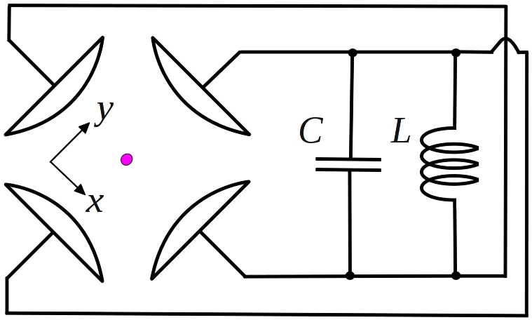
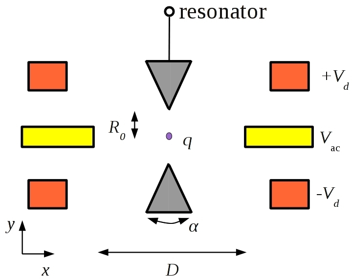
We consider a charged particle trapped in a harmonic potential. The particle is located between two sets of coupling electrodes which are connected to an electrical resonator, as in Fig. 1(a). The circuit couples to the position of a particle in the trap via the voltage on the coupling electrodes. The interaction energy is , where is the charge and the position of the particle, is the voltage between the coupling electrodes, and the potential at position , when 1 V is applied to the coupling electrode. For simplicity, here we consider coupling electrodes which create electric quadrupoles of the form , but the analysis can be generalized to potentials containing cross terms as well. For a displacement in the direction , around the trapping position, the potential can be expanded as Note Then, the Hamiltonian for the trapped particle and the circuit is, to second order in
| (1) |
Here, is the particle displamecement, is the particle canonical momentum. is the effective capacitance of the resonator at the coupling electrode. represents the flux variable at the coupling electrode, and is the canonically conjucate charge, which includes the charge, , induced on the electrode by the moving particle, and a classical, time-dependent charge , induced from the classical parametric drive voltage. The latter is detuned by the trap frequency, , from all resonant modes in the system and, as we discuss in Appendix C, this induced charge can be made negligibly small by carefully balancing the different electrode capacitances in the device.
The coupling term linear in position, , couples the circuit and the particle when the two are resonant, and the quadratic terms, , lead to parametric coupling. To switch on the parametric action, we drive classical particle motion, , in addition to the quantum motion in the trapping potential, . We decompose the particle position as . Expanding the quadrupole part of the interaction energy, we obtain the parametric coupling term , where is the quantum charge degree of freedom in the circuit. When driving motion in the direction, the Hamiltonian in the interaction picture now becomes
| (2) |
The , and operators correspond to the circuit and particle modes respectively, is the circuit resonant frequency, the particle frequency, , describes quantum fluctuations of the particle position, and quantum fluctuations of the circuit charge variable, which depends on the characteristic impedance .
If , then the terms of Eq. 2 survive in the rotating wave approximation . The system operates as a parametric frequency converter, with the classical drive providing pump photons which allow coherent coupling between the particle and the resonator. Population exchange between the two modes occurrs with a parametric coupling rate Louisell1961 . If , then the system behaves as a parametric amplifier Louisell1961 . The effective Hamiltonian then has the form which generates two-mode squeezing of the coupled modes Braunstein2005 .
In what follows, we focus on the former of these two cases. We also focus on electrons, which due to their large charge-to-mass ratio can couple very strongly to microwave circuits using currently attainable experimental parameters. In Sec. V we discuss applications of this scheme: i.e. quantum state initialization for the electron, creation of entanglement and quantum state transfer between single electrons and superconducting qubits, as well as creation of entanglement and quantum state transfer between distant elecrons.
III Electron trap and resonator design
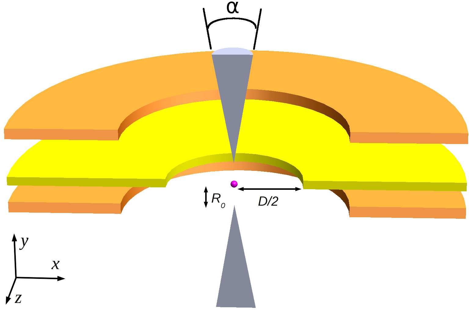
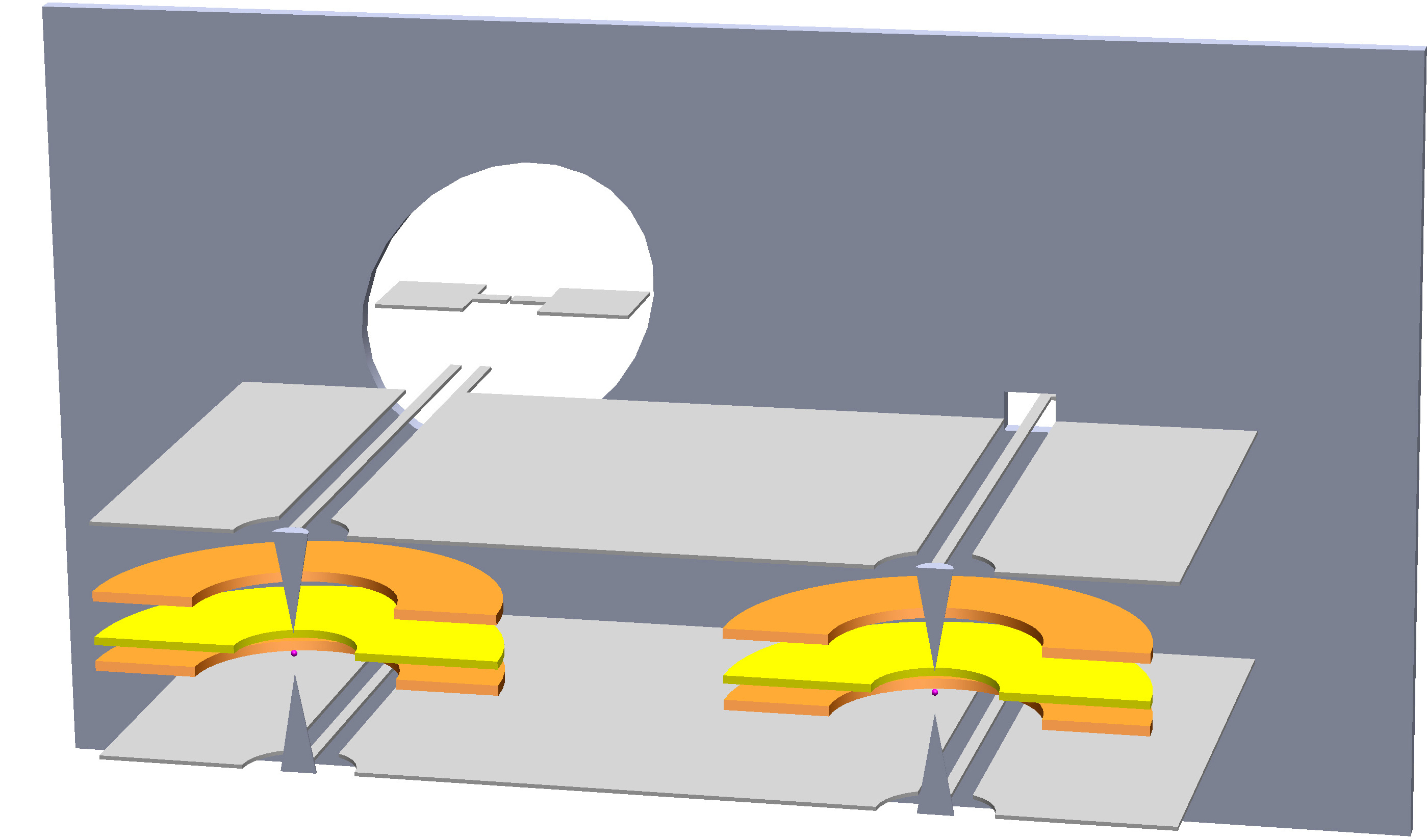
For simplicity, we choose a ring trap to trap single electrons (Fig. 2). This kind of trap combines high trap depth, low anharmonicity of the trapping potential, and strong parametric coupling. We simulated this design with 30 m, 5 m, 20o (see Fig. 2 for an explanation of the parameters) using an electrostatics solver Singer2010 . The effective coupling length appearing in Eq. 1 is 7.3 m. Single electrons with secular frequencies 500 MHz, 400 MHz, can be trapped with trap depth of 0pt using a trap drive on the central ring electrode (shown in yellow) at GHz, amplitude approximately 0.4 V, and with a static bias of a few hundred mV on the trap electrodes. To implement the parametric coupling scheme, we can drive electron motion in the direction at and 350 nm, by applying opposite oscillating voltages of amplitude 0.2 V on the top and bottom ring electrodes (orange). Numerical integration of the equations of motion shows that the trap is stable under this condition (see Appendix A). The trapping potential and the parametric pump drive will not significantly limit the fidelities of processes described in Sec. V, if they are stable to better than 1 part in . The capacitances between the tip electrodes and the ring electrodes in this structure range from 0.3 fF to 0.8 fF. While this will have only a small loading influence on the resonator to which the particle motion will couple, the resonator can be off-resonantly excited by the parametric drive and the trapping potential. We discuss solutions to these technical issues in Appendix C.
To load single electrons in the ring trap, one option is to have the trap fabricated at the end of a linear Paul trap with segmented electrodes Kielpinski2002 . The linear trap can have a taper from large trap dimensions to smaller dimensions Amini2010 to load electrons at high energy and resistively cool them Wineland1975 in different stages (e.g. precooling to 10 K, followed by cooling to 1 K to load into the ring trap). Electron clouds can be loaded in the linear trap using a heated filament, or, in order to have better control on the number of created electrons, by photoionization of an atomic vapor. After the electron cloud is cooled to 1 K, the number of electrons in the trap can be distinguished by coupling their motion to an electrical resonator at the electron resonance frequency Wineland1975 , and the segmented trap electrodes can be used to heat and split the electron cloud until a single electron is trapped Wineland1973 . Finally, the electron can be transported into the ring trap, and ‘locked’ in place by modifying the ponderomotive trapping potentials of the linear trap and the segmented trap Karin2011 ; Kumph2011 .
The resonator depicted schematically in Fig. 1 can be a lumped-element resonator, or a coplanar waveguide (CPW) resonator. The coupling strength between an electrical resonator and the particle in the trap will benefit from high characteristic impedance resonators, due to the dependence of quantum voltage fluctuations on the characteristic impedance . The effective impedance for a CPW section with length is related to the CPW characteristic impedance, , by Daniilidis2012 . In what follows, we consider a resonator with characteristic impedance 1 k. TiN-based high kinetic inductance resonators Zmuidzinas2012 are promising in this respect. Using this technology, resonators with very high inductance per unit length, exceeding , have been achieved DayPrivComm . Designing resonators based on such films, with gap between the center conductor and the ground plane in the tens of range would achieve the required impedance of approximately .
IV Decoherence sources
Provided a sufficiently low-noise classical drive, parametric frequency conversion can couple two non-resonant systems with no added noise Mishkin1969 . The fidelity of coupling between electrons and electrical circuits will be limited by motional decoherence of the electron motion, decoherence in the resonator and superconducting qubit circuits, and classical noise in the trap drive and the parametric drive.
To estimate the heating rate of the electron motion in the direction, we need to know the spectral density of electric field noise at 500 MHzDeslauriers2006a . Johnson noise and electronic technical noise can be made very small, so we focus on the so called ’anomalous’ heating, encountered in ion traps. The dominant contribution of this noise has been shown to arise from the electrode surfaces Hite2012 . We can model the noise as arising from a collection of independently fluctuating electrical-dipole type sources on the trap electrodes, in which case the noise level is determined by the surface density of electrical dipoles on the electrodes Daniilidis2011 ; Safavi-Naini2011 . In this model, the magnitude of the noise for a given density of dipoles has been shown to depend on the electrode geometry Low2011 . We take into account the non-planar geometry of the proposed trap as discussed in Appendix B. Based on heating rates measured in ion traps at 4 K Brown2011 , a single electron trapped at = 500 MHz will have s (heating of 8100 motional quanta/s) if the noise scales with frequency as , and s (heating at 690 quanta/s) if the scaling is , as observed in Hite2012 .
The internal quality factor () of CPW resonators is thought to be limited by fluctuating two-level systems (TLS) in the interface between the superconductor and the dielectric substrate on which it is fabricated Gao2007 ; Gao2008 ; Kumar2008 . As a result, decreases by 1 to 2 orders of magnitude as the the energy stored in the resonator decreases to the few photon level. In recent years, significant efforts in dielectric substrate cleaning and materials engineering have resulted in an increase of Wang2009 ; Vissers2010 , with values at the single photon level currently exceeding Megrant2012 . Moreover, it has been realized that the resonator losses can be limited by reducing the participation of the dielectric-superconductor interface in the resonant mode. One way to achieve this is by building higher characteristic impedance CPW resonators Geerlings2012 . This can prove advantageous for the high characteristic impedance resonators needed in our application. TiN-based high kinetic inductance resonators in the 1-2 GHz range, already mentioned in Sec. III, show very high quality factors LeDuc2010a , and due to their high kinetic inductance have wavelength significantly lower than the vacuum wavelength, which significantly reduces their radiative losses. In what follows, we assume a resonator with quality factor similar to the best value obtained by Megrant et al., with s at 7 GHz Megrant2012 .
The main goal of this work is to show how to couple an electron to a superconducting qubit, via the above mentioned resonator. We now discuss the superconducting qubit which currently exhibits the best coherence times, namely the ‘3-dimensional’ transmon qubit Paik2011 ; Rigetti2012 . The transmon is a ‘Cooper pair box’ qubit in which the Josephson junction capacitance is increased to make the device largely immune to charge noise Koch2007 . Recently, this kind of device has shown coherence times in the several tens of range by suppressing radiative and charge-flucutator related losses after placing the device inside microwave cavities Paik2011 ; Rigetti2012 . Here we focus on this implementation of superconducting qubits, and assume decoherence times and , as those in Rigetti2012 .
V Applications
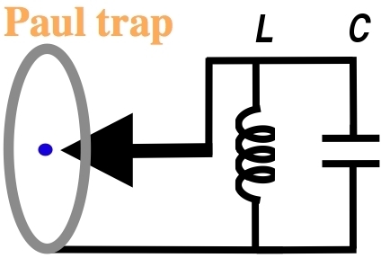
V.1 Electron-resonator coupling
In order to couple the electron to a microwave circuit, we consider the tip electrodes to be connected to the open end of a superconducting coplanar waveguide resonator (CPW), or a lumped element resonator (Fig. 3a). In the case of a CPW, quantization of the resonator mode can be treated as in Blais2004 . With trap frequency 500 MHz, driven motion 350 nm, 7 GHz, and , the coupling rate is 1.1 MHz. This allows complete population exchange between the motion of a single electron and a GHz resonator in 230 ns. By turning on the parametric coupling between an electron resistively precooled to K Heinzen1990 and a microwave resonator at 30 mK, for time , the electron motion can be prepared to its ground state with approximately 99.8% fidelity. The fidelity of this operation is limited by the heating of the electron motion during the swap operation, and can serve as a quantum-state initialization step in the context of QIP.
(a)
 (b)
(b)
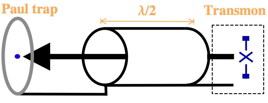
V.2 Electron-transmon coupling
For a specific example of a hybrid quantum device realizable under our scheme, we consider the case of coupling an electron to a transmon through an intermediary transmission line, as shown schematically in Fig. 3. The tips of the Paul trap are connected to the open end of a CPW resonator, which couples the electron oscillation to the resonator. The transmon is operated inside a 3 dimensional cavity, an architecture which provides increased coherence times Paik2011 . The second open end of the resonator extends into the cavity, allowing it to couple to the mode of the cavity with a rate 3 MHz (Appendix D). The transmon is very strongly coupled to the cavity, with coupling constant in the 100 MHz regime Paik2011 . The cavity-transmon detuning satisfies , i.e. the system is operated in the dispersive regime and the state that the resonator couples to is a dressed transmon state with transition frequency . Adiabatically eliminating the cavity, yields an effective coupling rate between the transmission line and the dressed transmon (Appendix E). The effective Hamiltonian for the electron-resonator-transmon system is:
| (3) |
where is the Pauli spin lowering operator for the transmon qubit, we have allowed for a detuning between the resonator and the transmon, and we choose a parametric drive in (Eq. 2). To optimize state transfer we choose such that .
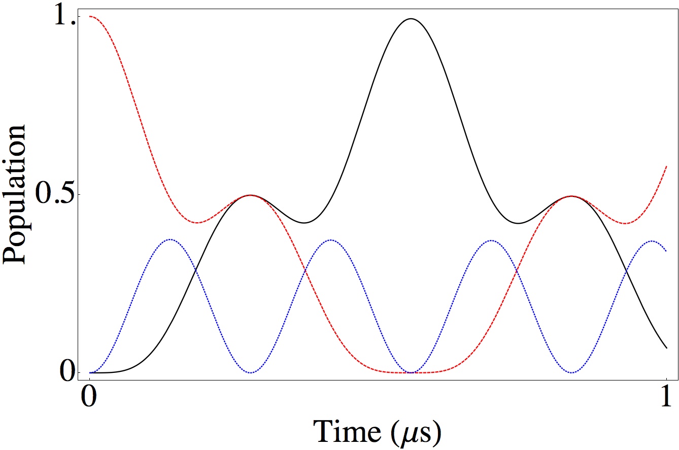
The detuning is necessary to produce maximally entangled states of the electron motion and the transmon (i.e. Bell states), and reduces the decoherence induced by losses in the bus. For an arbitrary detuning, this Hamiltonian will not generate complete state transfer between the electron and the transmon, because some population will, in general, be left in the transmission line. However, by choosing a “magic” detuning full state exchange will occur between the electron and the transmon in , and the two in a Bell state at . This situation is similar to the Mølmer Sørensen gate for trapped ions Sorensen2000b . Using the parameters quoted above for the electron traps and for the microwave resonator, electron-transmon state transfer is achieved in 560 ns. By numerically solving the Lindblad master equation of the coupled system (see Fig. 4), we find a fidelity for state exchange of for the magic detuning. At time 280 ns the electron and the transmon are in the Bell state with fidelity . With our set of parameters, these fidelities are limited mainly by losses in the bus and by heating of the electron motion. For the magic detuning, an electron-transmon swap operation is completed in 320 ns with fidelity 99.4%.
V.3 Electron-electron coupling
An additional application of this parametric scheme is in coupling electrons in separate traps via a microwave bus. If both ends of the CPW are connected to the coupling tips of two electron traps, the electron in each trap gets coupled to the microwave bus with parametric coupling constant . Using the same ’magic’ detuning idea as above and the parameters of Fig. 4, we find that the two motional states can be entangled with each other within 280 ns with fidelity , and swapped within 560 ns, with fidelity . For the magic detuning, an electron-electron swap operation is completed in 320 ns with fidelity 99.1%.
V.4 Spin-motion coupling
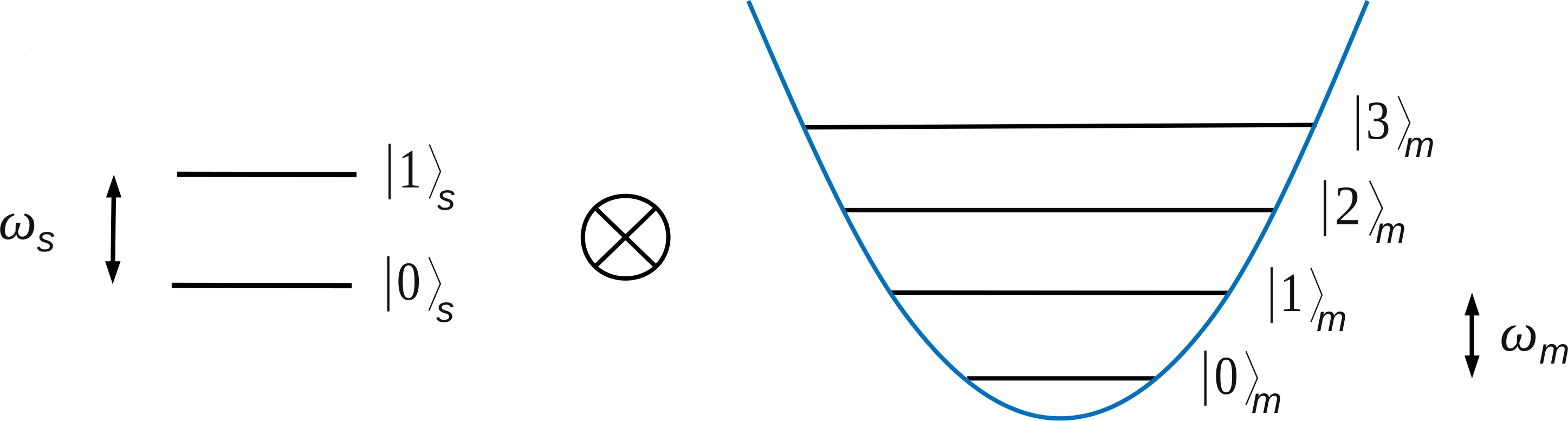
In order to take full advantage of the low decoherence of the trapped electron system, we now consider mapping the electron motional state to its spin. We can define an electron spin manifold with splitting in the radio-frequency range, e.g. 28 MHz using a static bias field of T, see Fig. 5(a). To do the state mapping, we consider the coupling mechanism implemented already with trapped ions Ospelkaus2008a ; Ospelkaus2011 . Microfabricated coils near the trap generate an oscillating magnetic field with frequency , thus driving a transition between the electron motion and its spin. Using a Helmholtz coil geometry with radius m, driven such that only a quadrupole magnetic field is generated at the electron, an oscillating current of 1 A, and frequency of 272 MHz can drive spin-motion transitions with Rabi frequency kHz. Here, we assumed again 500 MHz, and 28 MHz, corresponding to a static bias field of T. The electron motional state can be mapped onto the spin in approximately 610 ns, with fidelity. The coils which generate the oscillating magnetic fields can be thermally anchored on a 1 K refrigeration stage to minimize heat load on the 30 mK stage, which is necessary for the superconducting electronics.
In order to preserve the phase coherence of the electron spin, the magnetic field at the electron needs to be stabilized. By stabilizing the magnetic field to 14 , the coherence time of the electron spin will exceed 1 s. This noise requirement is rather modest, it is three orders of magnitude less stringent than those achieved with magnetic field shielding in SQUID magnetometry Robbes2006 . Heating of the electron motion in a spatially inhomogeneous magnetic field will cause additional dephasing. This can be mitigated by engineering a homogeneous static magnetic field, and by periodically cooling the electron motion to its ground state.
VI Outlook
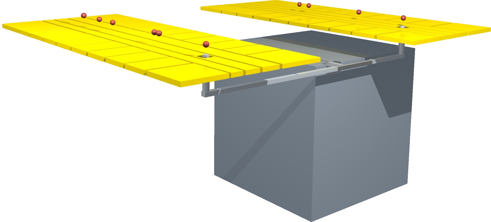
The elementary toolbox described above can be used in hybrid QIP platforms in which the electron spin serves as a quantum memory, and the electron motion as a bus for coupling to superconducting circuits, see Fig. 5. One possibility is for the transmon qubits to function as processing units, and the electron spins to serve as a quantum memory (Fig. 5b). A second possibility is to use the trapped electrons as both processing and memory units, with the transmon serving as a state readout device. A third option uses moving electron qubits in segmented linear Paul traps, much the same way in which ion-trap based scalable QIP is pursued (Fig. 5c) Kielpinski2002 ; Hanneke2009a .
The first two types of architecture can be implemented using the building blocks shown in Fig. 5(b). In both cases, the LC resonator-based ground state cooling of the electron, and the magnetic-field based spin-motion coupling serve to initialize the electron state. If the superconducting qubits are used for information processing, the operation between electron and transmon allows information exchange between the processing and memory qubits. In the case of electron-based QIP, operations allow transfer of information between different nodes. Single qubit rotations can be performed on the electron spin, which together with the gates between the motion of different electons offer a universal set of gates. One way to read out the state of the electron is by coupling the electron motion to a dressed three-dimensional transmon, as described above, but alternative architectures would be sufficient for this task. In fact, coherently swapping the electron motion with the field of a microwave resonator opens the possibility of coupling the electron to any type of superconducting non-linear device which can be coupled to microwave resonators.
(a)
 (b)
(b)
 (c)
(c)
The third distinct architecture which becomes possible using the toolbox described here uses moving electron qubits. Our proposed parametric frequency conversion mechanism can be applied to linear microfabricated Paul traps for electrons, similar to the ones extensively pursued for trapped ions Hanneke2009a . In this case, ground state cooling of the electron motion, state initialization, and readout of the electron spins can be based on microwave circuits. Two-qubit entangling gates can be performed using a microwave bus, the direct Coulomb interaction between nearby electrons Ciaramicoli2003 , or with microwave gates Ospelkaus2008a . Finally, non-linear superconducting circuits can be used to read out the state of the electrons. This approach will not require lasers for cooling, manipulating, and detecting the electron qubits, as trapped-ion based approaches do. In addition, it can be significantly faster than current ion-trap based approaches. State initialization and read-out can be performed on the order of a few s, roughly two orders of magnitude faster than with ions. Owing to the higher electron frequencies, particle transport can also be two orders of magnitude faster. Two-electron gates based on the Coulomb interaction of nearby electrons, will be limited by the rate of spin-motion coupling that can be achieved. This can be more than one order of magnitude faster than the values achieved with ions, due to the larger extent of the electron’s wavefunction.
As a final, longer-term application, we consider the possibility of scaling an architecture similar to that of Fig 5(c) to sub-micrometer dimensions, and operating it entirely on a 1 K refridgeration stage. This would allow fast gate operation times and overcome the problem of limited cooling power, typically in the sub-mW range, which dilution-refrigerator based approaces face. Miniaturized linear Paul traps for electrons, with typical electron-electrode distances of 500 nm could achieve secular frequencies of GHz and depths of 10 meV, with moderate trapping voltages of less than 1 V. The parametric upconversion mechanism, described in Sec. II, applied to this case would allow coupling to superconducting resonators with frequencies above GHz Goy1983 ; Zmuidzinas1994 enabling ground-state cooling of the electrons in ns. Electron transport, swapping and entangling gates could be performed in time of order 0.1 ns. To read out the electron motional state, mapping to a superconducting qubit, as outlined above, is one option, but an alternative option would be dispersive circuit-CQED type read-out Blais2004 on the {} manifold of the electron motion. A number of technical challenges would need to be overcome in such an approach. Device miniaturization will not be feasible before the electrode surface noise sources are eliminated at cryogenic temperatures, for example reduction by three orders of magnitude over current values would imply electron heating rates of order quanta/s in the example mentioned here. In addition, the technology of millimeter wave sources and resonators in the millimeter frequency band, above 100 GHz, would need to be adapted to the high-fidelity, low-loss demands of QIP applications.
In summary, we have proposed a parametric frequency conversion scheme which can couple the motion of trapped particles to solid-state
quantum circuits, and does not rely on non-linear solid-state devices. This scheme allows swapping and entangling operations between electrons and superconducting
electronics, and can be used to initialize and read-out the state of an electron, as well as to use the electron spin as a quantum memory for superconducting qubits.
Using current parameters for the device components we find that all basic operations necessary for QIP can be carried out with fidelities close to 99%.
We have described applications of this scheme to hybrid quantum architectures in which both trapped electron spins and transmon circuits serve as processing
qubits. Our toolbox enables a QIP architecture with electrons, similar to the one currently pursued with trapped ions in segmented traps, but having advantages
in speed and scalability.
We would like to acknowledge useful discussions with I. Siddiqi, K. Murch and with P. K. Day. This research was funded by the ODNI, IARPA, through the ARO grant 30378, by AFOSR through the ARO grant FA9550-11-1-0318, by NSF under NSF-DMR-0956064, NSF-CCF-0916303, and by Agilent under ACT-UR 2827. All statements of fact, opinion or conclusions contained herein are those of the authors and should not be construed as representing the official views or policies of IARPA, the ODNI, or the U.S. Government.
Appendix A Parametric drive of the electron motion
As discussed in the main text, the parametric coupling can be switched on by driving classical electron motion. Electron motion can be driven in the direction, but also in the direction. To achieve the latter, we can split the trapping ring electrode into two half rings on the sides of the plane, and apply a classical out-of-phase drive to the two sides. This option comes at the expense of a factor of 2 reduction in the parametric coupling rate and here we focus on driving the motion. The trap drive and the parametric drive of the electron motion are detuned from the superconducting electronics by 500 MHz. In order to drive electron motion in the direction at GHz and 350 nm, we apply an oscillating voltage of amplitude 0.2 V on the ring electrodes labeled in Fig. 6 below. Numerical integration of the electron equations of motion, with both the trapping potential at and the drive at , shows that the trap is stable, and motional sidebands appear at frequencies . If only sidebands at are present, and this can be a preferable configuration.
It is interesting to consider the limits of applying the proposed parametric scheme to trapped ions, by analyzing the influence on the trapping pseudopotential when . The parametric pump field generates a pseudopotential which is not significant for electrons under the trapping conditions we described above. The situation is different for ions, because of their lower secular frequencies. To see this, we compare two energy scales: The strength of the pseudopotential, , which arises from the parametric drive when the driven motion amplitude is , and the trapping potential with curvature . The ratio of the two is . So the pseudopotential arising from the parametric drive scales quadratically with the driven motion amplitude, and with the frequency step-up. For example, for 9Be+ with secular frequency of 2 MHz in a trap such as the one descirbed here, the limiting frequency for 350 nmis approximately GHz. For higher frequencies it becomes hard to control non-linearities in the trap potential.
Appendix B Decoherence of the electron motion
To estimate the effect of fluctuating electrical-dipole like noise sources on the trap electrodes, we incoherently sum the contributions of all dipoles on the surface of the electrodes. For each one of the conical tips with opening angle , we find that the noise is reduced over the noise generated by a flat surface. For low opening angles the noise level at distance from the tip is well approximated by
| (4) |
where is the noise at a distance from a flat surface (i.e. a cone of opening angle ). Similarly, for a ring electrode similar to the one in Fig. 1, the noise contribution is estimated at
| (5) |
i.e. each one of the top and bottom surfaces of the ring contributes the same noise as a flat plane located a distance from the ion (), and the inside surface of the ring contributes a fraction of that noise. The two rings which are used to drive the electron motion (orange in Fig. 2) can easily be placed a factor of 2 or more further away from the ion compared to the trapping ring electrode, and their contribution can thus be neglected. Taking these results into account, and based on the noise value measured in cryogenic traps Brown2011 , the heating rate for an electron trapped at 500 MHz in the ring trap discussed here, is estimated at 8100 motional quanta/s if the frequency scaling of the noise is , and at 690 quanta/s if the scaling is .
Appendix C Capacitive coupling of classical signals to the quantum bus
In the geometries outlined in Fig. 2 and Fig. 3, the classical drive used to trap the electrons and to pump the parametric action can couple to the CPW used as a quantum bus, and cause off-resonant excitations. Conversely, if the CPW couples to the transmission lines used to drive the trap and the parametric action, then it will radiatively decay into the transmission lines. To minimize these effects, one needs to capacitively drive opposite ends of the CPW resonator (Fig. 3b) in such a way that the most of the capacitive coupling cancels out, or use some equivalent scheme. Capacitive coupling of the CPW to a 50 feed line or LC resonator used to drive the trap electrodes will only limit the quality factor at the level if the coupling capacitance is limited to below 0.2 fF. Here we describe a scheme which is mainly aimed at cancellation of the off-resonant excitation, while achieving far greater reduction of the radiative losses.
To minimize off-resonant excitations, we need to carefully balance capacitances in the device and weakly couple in an additional ‘fine-tuning’ signal. One possible solution is outlined in Fig. 7. The signal, which is capacitively coupled via a parasitic capacitance , to the coupling electrode, is also coupled with an appropriate amplitude to the opposite end of the resonator, via the balancing capacitance . Both capacitors are connected to a resonator with characteristic impedance , and moderate quality factor , which is used to drive the trap electrodes, and helps minimize radiative losses of the resonator. An additional 50 transmission line is capacitively coupled with to one end of the resonator, and driven with an adjustable amplitude and phase shift, in order to fine-tune the cancelation of the off-resonant excitation. The parasitic capacitances in the ring trap described here are on the order of 0.5 fF, and if they are balanced to , the off-resonant excitation of the resonator will amount to approximately 200 photons. To fine-tune the cancellation to the level of photons, the amplitude and phase in an adidtional 50 line, coupled by needs to be adjusted at the 0.4 mV level, provided the phase is controlled to better than 10o.
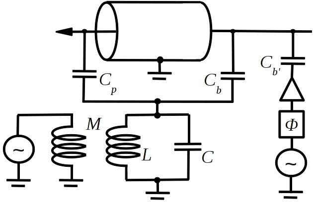
This configuration also minimizes the inverse effect of radiating from the CPW into the classical-signal transmission lines. Due to the use of an LC resonator which is far detuned from the CPW bus and of a weakly coupled transmission line, the radiative loss of the CPW to the external lines will be limited to the level of .
Appendix D Electrical resonator and cavity interaction
In order to couple the coplanar waveguide transmission line to the transmon cavity, perhaps the simplest option is for the center conductor and one side of the ground plane of the line to extend into the cavity, with an appropriate modification in geometry to maintain the impedance of the transmission line constant. To estimate the interaction strength of the TEM mode of the CPW to the mode of the cavity, we treat the transmission line as a collection of electrical dipoles formed between the center conductor and ground. The dipoles arise from the local charge density on the CPW and they form a continuous distribution over its length. A segment of length along the line direction () has dipole strength . Here is the spacing between the CPW center and signal return conductors is the magnitude of charge fluctuations in the line, and is the wavelength of the wave in the CPW. If the electric field of the cavity mode, , is aligned with the dipoles (i.e. if it is along the line connecting the center conductor to ground), then an upper limit for the coupling strength can be expressed as the integral , where is the magnitude of electric field fluctuation in the cavity, and the effective length can be up to order .
We consider a cavity at 7 GHz, and a CPW with effective impedance of 1 k. A lower limit for is m, which implies that can be 10 MHz, for . Our architecture requires lower values, in the 3 MHz range, which can be achieved with appropriate design.
Appendix E Electron-transmon quantum electrodynamics
The electron-transmon system is at heart a problem of four coupled quantum systems: three oscillators and a qubit. The electron motion, intermediate quarter wave resonator, and transmon cavity function as harmonic oscillators, while the transmon acts as a qubit. It is illustrative to write the effective four-system problem by an effective Hamiltonian
| (6) |
with , the vector of excitation annihilation operators for the electron, transmission line, transmon cavity, and transmon respectively. For presentation, we have absorbed all the time-dependent factors into the definitions of and . Such a formulation is useful because the coupling matrix contains the relevant dynamics. The excitation energies are read off from the diagonal elements, and the coupling rates are read off from the off-diagonal elements.
In the limit where the cavity-transmon coupling is the strongest (), we can view the eigenstates of the cavity-transmon system as the modes of interest, and focus on coupling to the transmon dressed state. Then, the problem can be reduced to an effective three-system problem in the following way. First, we diagonalize the cavity-transmon block in the limit . After the diagonalization we get two vectors: one with a projection mostly onto the transmon mode (which we referred to as the ’dressed transmon’), and with a projection onto the cavity mode only of order . The second has a projection mostly onto the cavity mode and projects onto the transmon mode also to order .
The first vector represents the operator . This is a Hamiltonian operator for a dressed transmon mode. The second vector is similar, representing a mode which lives primarily in the cavity. Since we have earlier chosen the cavity to be far detuned from the transmon, this mode can be adiabatically eliminated. Removing this dressed cavity mode from the basis produces a reduced coupling matrix
| (7) |
By adjusting and so that ,
we can obtain complete state transfer and entanglement between the electron motion and the dressed transmon, as we discuss in the main
text.
References
- (1) DiVincenzo D P 2000 Fortschr. Phys. 48 771–783
- (2) Ladd T D et al. 2010 Nature 464 45–53 ISSN 1476-4687
- (3) Häffner H et al. 2008 Phys. Rep. 469 155
- (4) Sørensen A S et al. 2004 Phys. Rev. Lett. 92 063601
- (5) Ciaramicoli G et al. 2003 Phys. Rev. Lett. 91 17901
- (6) Tian L et al. 2004 Phys. Rev. Lett. 92 247902
- (7) Daniilidis N and Häffner H 2012 Ann. Rev. Cond. Matt. Phys. 4 83-112
- (8) Heinzen D J and Wineland D J 1990 Phys. Rev. A 42 2977
- (9) Kielpinski D et al. 2012 Phys. Rev. Lett. 108 130504
- (10) Pollack S et al. 2008 Phys. Rev. Lett. 101 071101
- (11) Pashkin Y A et al. 2009 Quant. Inf. Proc. 8 55–80
- (12) Wineland D J and Dehmelt H G 1975 J. App. Phys. 46 919
- (13) Walz J et al. 1995 Phys. Rev. Lett. 75 3257–3260
- (14) Hoffrogge J et al. 2011 Phys. Rev. Lett. 106 1–4
- (15) Wineland D J et al. 1998 Jour. Res. Nat. Inst. Stand. Tech. 103 259–328
- (16) Deslauriers L et al. 2006 Phys. Rev. Lett. 97 103007
- (17) Brown K R et al. 2011 Nature 471 196–9
- (18) Schuster D I et al. 2010 Phys. Rev. Lett. 105 040503
- (19) Hite D A et al. 2012 Phys. Rev. Lett. 109 103001
- (20) Bushev P et al. 2011 Eur. Phys. Jour. D 63 9–16
- (21) Here, the terms of odd order in and can be made vanishingly small by symmetry, and the higher than quadrartic terms in can be made negligibly small.
- (22) Louisell W et al. 1961 Physical Review 124 1646
- (23) Braunstein S L and Loock P V 2005 Rev. Mod. Phys. 77 513–577
- (24) Singer K et al. 2010 arxiv:0912.0916v
- (25) Kielpinski D et al. 2002 Nature 417 709–711
- (26) Amini J M et al. 2010 New Jour. Phys. 12 033031
- (27) Wineland D J et al. 1973 Phys. Rev. Lett, 31 1279–1282
- (28) Karin T et al. 2011 Appl. Phys. B 106 117
- (29) Kumph M et al. 2011 New Jour. Phys. 13 073043
- (30) Zmuidzinas J 2012 Ann. Rev. Cond. Matt. Phys. 3 169–214
- (31) Day P K private communication
- (32) Mishkin E A and Walls D F 1969 Phys. Rev. 185 1618
- (33) Daniilidis N et al. 2011 New Jour. Phys. 13 013032
- (34) Safavi-Naini A et al. 2011 Phys. Rev. A 84 023412
- (35) Low G H et al. 2011 Phys. Rev. A 84 053425
- (36) Gao J et al. 2007 Appl. Phys. Lett. 90 102507
- (37) Gao J et al. 2008 Appl. Phys. Lett. 92 152505
- (38) Kumar S et al. 2008 Appl. Phys. Lett. 92 123503
- (39) Wang H et al. 2009 Appl. Phys. Lett. 95 233508
- (40) Vissers M R et al. 2010 Appl. Phys. Lett. 97 232509
- (41) Megrant A et al. 2012 Appl. Phys. Lett. 100 113510
- (42) Geerlings K et al. 2012 Appl. Phys. Lett. 100 192601
- (43) Leduc H G et al. 2010 Appl. Phys. Lett. 97 102509
- (44) Paik H et al. 2011 Phys. Rev. Lett. 107 240501
- (45) Rigetti C et al. S T, Rozen J R, Keefe G A, Rothwell M B, Ketchen M B and Steffen M Phys. Rev. B 86 100506(R)
- (46) Koch J et al. 2007 Phys. Rev. A 76 042319
- (47) Blais A et al. 2004 Phys. Rev. A 69 062320
- (48) Sørensen A S and Mølmer K 2000 Phys. Rev. A 62 022311
- (49) Ospelkaus C et al. 2008 Phys. Rev. Lett. 101 90502
- (50) Ospelkaus C et al. 2011 Nature 476 181–184
- (51) Robbes D 2006 Sens. Act. A: Physical 129 86–93
- (52) Hanneke D et al. 2009 Nat. Phys. 6 13–16
- (53) Goy P et al. 1983 Phys. Rev. Lett. 50 1903
- (54) Zmuidzinas J et al. 1994 IEEE Trans. Microwave Th. Techn. 42 698