Perfect memristor: non-volatility, switching and negative differential resistance
Abstract
We propose a simple model of a nanoswitch as a memory resistor. The resistance of the nanoswitch is determined by electron tunneling through a nanoparticle diffusing around one or more potential minima located between the electrodes in the presence of Joule’s heat dissipation. In the case of a single potential minimum, we observe hysteresis of the resistance at finite applied currents and a negative differential resistance. For two (or more) minima the switching mechanism is non-volatile, meaning that the memristor can switch to a resistive state of choice and stay there. Moreover, the noise spectra of the switch exhibit crossover, in agreement with recent experimental results.
Fast progress in flash memory suggests that standard magnetic hard drives will soon be replaced by faster and much more reliable solid state drives silicon . However, solid state drives are still very expensive and their capacitance is very limited when compared with magnetic drives. To overcome these limitations, a new generation of flash-like memory has to be developed book .
A most promising candidate for very fast and high density memory are nanomemristors (memory-resistors) stan . In particular, resistive switching was observed in binary oxides, like TiO2, NiO and perovskite oxide memristors. Memristive switches would provide a viable solution for dense memory, logic, and neurocomputing, if they can be demonstrated to advantageously scale with size, power, and driving voltage, and perform without failure and fatigue in a repeatable and uniform manner. Some of these issues are not well understood although the hysteretic behavior of such materials, especially thin films of transition metal oxides like Ta2O5, Nb2O5, TiO2, NiO, Cu2O in metal-insulator-metal vertical devices has been known for decades 1 . In recent years, the interest in various oxide-based systems switchable by electric pulses has grown dramatically 2 ; 3 ; 4 leading to important breakthroughs, despite a still poor understanding of the switching mechanisms and, in particular, of the joint heat-electron-ion transport at the nanoscale.
Molecular dynamics simulations 5 ; 6 of interacting oxygen vacancies have demonstrated the formation of vacancy filaments and clusters characterized by a certain degree of orientational order. This picture is in qualitative agreement with recent measurements 7 , which hint at the existence of localized conducting channels. Moreover, the formation of nanoswitches (buried atomic junctions) between large clusters of vacancies would be consistent with the observed quantum conductance and the unusual resistance-noise spectrum in TaOx memristors 6 . The question then arises to what extent nanoswitches formed in oxide memristors are responsible for resistive switching and how to effectively control switching in such nanojunctions.
In this Letter, we consider the simplest possible model of joint electron-ion-heat dynamics for a nanoswitch with electrons tunneling through a bridging nanoparticle (either an ion or a vacancy) subject to thermal fluctuations. Electric current through the switch produces Joule heating, which results in local temperature relaxation, described by Newton’s cooling law. Surprisingly, we demonstrate that this system admits two distinct resistive states even if the nanoparticle has only one mechanical attractor (e.g., the particle moves in a potential with a single minimum). Moreover, if the particle is confined by a potential with, say, two minima, these two resistive states can survive even at zero applied current (or voltage), so that the junction could serve as a non-volatile resistive switch. Furthermore, by applying current-voltage pulses such a memristor can be made switch into the desired resistive state, almost deterministically, although the particle is subject to random forces, only. Therefore, the resistance of this switch can be cycled through its hysteresis loop in apparent analogy with the elementary mechanism of magnetic memory devices. In this regard, our model exhibits all key features of a resistive memory device.

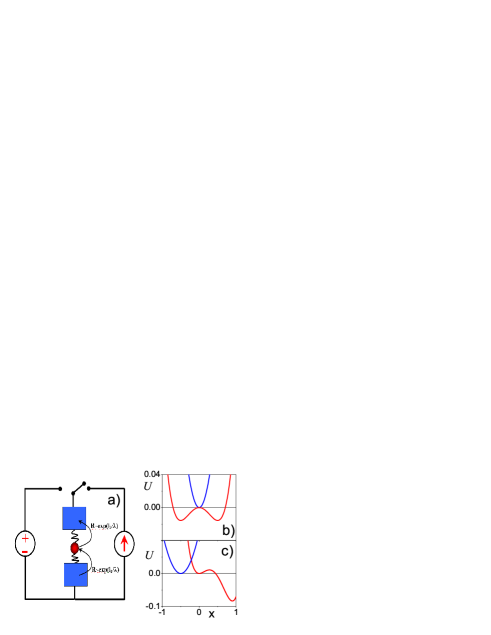
Model.— Let us consider a nanoparticle diffusing between two electrodes subject to thermal noise (Fig. 1a). An electric current through the switch sets on when the electrons tunnel from one electrode to the other via the nanoparticle. Here, we assume electron relaxation to be much faster than heat diffusion and the nanoparticle dynamics, thus, ignoring any shuttling effects shuttle . Therefore, the instantaneous resistance of the device, , is a function of the particle location, , whereas its temperature, , results from the balance between Joule heating, which depends on , and temperature relaxation. This simplified electron-particle-heat dynamics can be formulated as
| (1) | |||
| (2) |
where is the dimensionless coordinate of the nanoparticle, which is confined by the binding potential between the two electrodes at (normalization condition). The random force represents a Gaussian, zero-mean, white noise with . In Eq. (2) the time dependence of the temperature is described by the standard Newton’s cooling law with Joule heat source , and being the junction heat capacitance and the temperature relaxation rate, respectively. The tunneling resistance between the first electrode and the particle and the particle and the second electrode are, respectively, and , where is the normalized norm tunneling length. The total switch resistance can be rewritten as , where is a dimensionless resistance and is the junction resistance when the particle is located at the midpoint between the electrodes, . If the particle is driven by an electrical current , Joule’s law states that , while in the case of voltage driven switches, . Correspondingly, in compact notation, , with and or , respectively, for current or voltage driven switches. The most interesting working regimes occur when the temperature relaxation is either slow, or fast, .
Slow temperature relaxation.— For a qualitative analysis in the slow relaxation regime, the resistance can be averaged with respect to the fast thermal fluctuations of the particle, , so that Eq. (2) can be reduced to
| (3) |
with stationary points satisfying the identity .
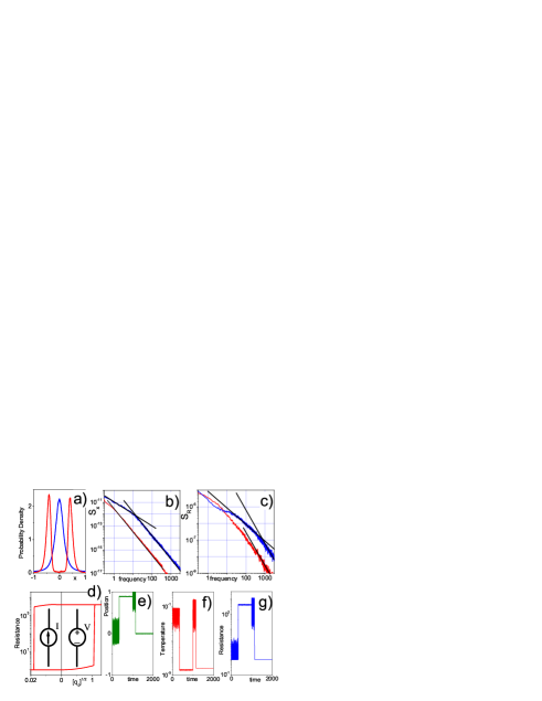
We start our analysis by assuming that the nanoparticle moves in a simple harmonic potential [Fig. 1(b)]. For a voltage driven memristor (), there is only one stationary point and no hysteresis is observed. In contrast, for a current driven memristor (), there are either one (stable) or three (two stable and one unstable) stationary points. The equation is graphically solved in Fig. 2(a). By simulating Eq. (1) at constant , we determined the curves (red solid curve). For [ and correspond to the upper and lower dashed straight lines in Fig. 2(a)], a straight line (dotted) crosses in three points; for all other the straight line and the curve cross in one point, only. The profile of the curve can be sketched analytically by noticing that the average must be taken with respect to the Boltzmann distribution density for and zero overwise. It follows immediately that the curves grow exponentially like at low temperatures, , and saturate at for high temperatures, , in agreement with our simulations [Fig 2(a)]. Therefore, within the interval , one can expect two stationary solutions of Eqs. (1) and (2) and hysteresis of both temperature and resistance, when the applied electrical current is cycled. These conclusions are confirmed by the numerical integration of the coupled Eqs. (1) and (2) for [Fig. 2(b)]. The characteristics curve displayed there, (note that ), exhibits hysteretic behavior, thus suggesting that this system can serve as a memory bit with two logic states corresponding to two different resistances. However, such a bit is not a non-volatile memory element, yet, since the two states exist only for a nonzero current (i.e., ).
The resistance hysteretic loop gradually shrinks as the position of the potential minimum of shifts away from the sample center, where has its minimum. More interestingly, negative differential resistance (NDR) was observed for . Indeed, at relatively large [Fig. 1(c)], the resistance first decreases with the current [Fig. 2(c), top red curve] and then increases for higher currents. With decreasing , the NDR region shrinks and finally disappears; on further lowering , resistance hysteretic loops open up and expand (Fig. 2(c), two bottom curves). NDR is due to the fact that on increasing the sharp peak of (which is centered around the potential minimum but far away from the minimum) broadens; correspondingly, on increasing the current the particle is allowed to dwell longer in the vicinity of the resistance minimum at .
In order to use our device as a non-volatile memory element, the nanoparticle must be confined to a potential with two wells at least. Below we analyzed in detail the case of the potential with two minima. Parameters control locations and depth of the minima. Hereafter, we will consider either even potentials with [Fig. 1(b)] or asymmetric potentials [Fig. 1(c)] with left minimum in the middle, , and right minimum at , i.e., near the r.h.s. electrode.
For slow temperature relaxation, , Fig. 2(d) clearly shows how the resistance hysteresis gets suppressed with increasing the depth of the potential minima at : The looped blue curves of vs. evolve into univalued curves – a “virgin” branch showing up only if the nanoparticle was initially located in the central well. Therefore, current cycling (or current pulse) allows switching the system from the low (nanoparticle sitting in the central well) to the high resistive state (particle being located near an electrode), but not vice versa!
Fast temperature relaxation.— Let us consider now the case of fast temperature relaxation, . For a qualitative analysis, we can assume that the temperature is always stationary with . Substituting this expression into Eq. (1) for the particle diffusion, we derive the Stratonovich stochastic equation
| (4) |
This equation can be regarded as a model for a Brownian particle diffusing through a medium with spatially varying temperature (or diffusion coefficient). For a current driven memristor, , the temperature reaches its maximum when the particle is located near the electrodes, , while for the a voltage driven memristor the highest temperature occurs when the particle sits around . Therefore, by applying current or voltage pulses, we can “heat up ” the center of the device or the regions near its electrodes, respectively. This effect can be invoked to reliably switch the device between low and high resistive state, with little regard for the parameters of the current or voltage pulses. Thus, a key problem in memristor design can be solved based on the present proposal.
We now propose a switching protocol for our model memristor with asymmetric potential having minima in the center, , and close to the right electrode, , namely , , and . Let us assume that the system is initially in the low resistive state. With increasing voltage, , the memristor switches to the high resistive state as shown in our simulations [Fig. 3(d); right side of the loop driven by a voltage source]. Upon decreasing the voltage to zero, the system sets in its high resistive state, indicating that the particle is now trapped near the right electrode. If we next increase the current, , the system switches to the low resistive state [Fig. 3(d); left side of the loop driven by current source]. By finally turning the current off, the resistance remains set to its low value. The loop being almost deterministic, the proposed switching protocol is clearly repeatable.
In order to illustrate the underlying switching dynamics, we computed , , and by numerically integrating the coupled Eqs. (1) and (2) and switching from (voltage driven) to (current driven) at . This mimics the sequence of voltage pulse, with duration , followed by a current pulse for [Fig. 3(e)-(f)]. Under the action of a constant voltage, , the initial low resistive state results in strong Joule heating, and, therefore, high temperature [Fig. 3(f)] and strong fluctuations of the nanoparticle position [Fig. 3(e)] just after applying a voltage pulse. However, as soon as the particle hops over the barrier and gets trapped in the well near the right electrode, the resistance increases and the heat production drops so fast that the particle temperature and its spatial fluctuations get quenched [Fig. 3(e)-(f) for ]. No further dynamics was observed over time until after the current pulse was applied for . Therefore, this switching mechanism is robust with respect to voltage pulse duration: Indeed, while the memristor is driven by the voltage pulse, the particle cannot hop back to the minimum at , being the temperature felt by the particle near the electrode very low. When a current pulse is applied, , the heat production starts anew because the particle is now in a high resistive state and Joule’s heating is proportional to the switch resistance, . As a result, the temperature sharply increases and the particle starts to fluctuate around the minimum near the electrode [Fig. 3(e) for just after ]. Eventually, the particle jumps into the central potential minimum where the resistance is the lowest. At that very moment the heat production drops and the particle gets stuck at ; no more changes are expected as the particle temperature is now very low. A strong enough current pulse, irrespective of its duration, suffices to switch the system back to its low resistive state and keep it there.
Pulse driven switching in our model turns out to be so effective because resistance and heat production strongly correlate with the particle location and the particle is always attracted toward the region with the lowest heat (or entropy) production, where it gets trapped. This conclusion can be easily extended to the case of any memristor with two distinct resistive states with resistances and such that . As a non-equilibrium thermodynamic system tends to attain a state of lowest entropy production, a voltage pulse will switch the memristor to the high resistive state , while a current pulse will switch it back to the low resistive state . Thus, our conclusions about optimal switching sequence are very general and can be readily extended to more elaborated memristor models.
Finally, we stress that the memristor switching mechanism proposed here can be regarded as an instance of noise-induced phase transition noise-induced . Such a stochastic dynamical phenomenon takes place when the minimum of the temperature does not coincide with the minimum of the binding potential, : The Brownian particle tends to dwell about the potential minima at low temperatures, and about the temperature minima at high temperatures, thus switching location on increasing the noise. In order to detect a noise-induced transition in our memristor model, we simulated the coupled Eqs. (1) and (2) for a symmetric double well potential with , and , in the current driven regime with (fast temperature relaxation) [Fig. 3(a)]. For weak currents, the stationary temperature is low and the particle is mostly localized around the potential minima; the corresponding distribution, , is doubly peaked (red curve). At higher currents, the temperature increases until the particle is pushed out of the potential wells toward the center of the sample, where the potential has a maximum, but the temperature is much lower. In the fast relaxation regime of Eq. (4) such a transition is well described by stationary probability distribution , where and is a normalization constant. A current increase is accompanied by a temperature surge, so that the minimum of the distribution at can change to a maximum noise-induced . More interestingly, the spectra of the resistance and position fluctuations (also called noise) show a qualitative change in correspondence with such a transition: The standard spectra break up into a low-frequency branch and a high-frequency tail [Fig. 3(b),(c)]. The unusual experimental noise spectra reported in Ref. 6 can thus be interpreted as the signature of a noise-induced transition occurring in TaOx memristors.
Conclusion.— The resistive switch model discussed here is expected to ensure the much sought-for properties of controllability and reliability one needs to design and prototype switchable nanomemristors for future flash memory devices. On the other hand, based on numerical simulation, we claim that its response to external current and voltage signals reproduces well a wide variety of experimental observations reported in the literature for real memristors. Moreover, the predicted phenomenon of negative differential resistance can considerably enhance the functionality of these nanostructures.
We acknowledge many fruitful discussions with R.S. Williams, who strongly supported this work. S.E.S. also acknowledges The Leverhulme Trust for partial support of this research; F.M. aknowledges partial support from the European Commission, grant No. 256959 (NanoPower).
References
- (1) L. Venema, Nature 479 309 (2011).
- (2) B. Dipert, M. Levy Designing with Flash Memory (Annabooks, San Diego, 1993).
- (3) J. Palmer, Science and technology reporter, BBC News, 16 May 2011: http://www.bbc.co.uk/news/science-environment-13392857.
- (4) G. Dearnaley, A.M. Stoneham, and D.V. Morgan, Rep. Prog. Phys. 33, 1129 (1970).
- (5) D.B. Strukov, G.S. Snider, D.R. Stewart, and R.S. Williams, Nature 453, 80 (2008); K. Szot, W. Speier, G. Bihlmayer, and R. Waser, Nature Materials 5, 312 (2006).
- (6) J.J. Yang et al., Nat. Nanotechnol. 3, 429 (2008)
- (7) J.J. Yang, F. Miao, M.D. Pickett, D.A.A Ohlberg, D.R. Stewart, C.N. Lau, and R.S. Williams, Nanotechnology 20, 215201 (2009).
- (8) S.E. Savel’ev, A.S. Alexandrov, A.M. Bratkovsky, and R.S. Williams, Nanotechnology 22, 254011 (2011); S.E. Savel’ev, A.S. Alexandrov, A.M. Bratkovsky, and R.S. Williams, Appl. Phys. A 102, 891 (2011); S.E. Savel’ev, A. S. Alexandrov, A.M. Bratkovsky, and R.S. Williams, Appl. Phys. Lett. 99, 053108 (2011).
- (9) Wei Yi, S.E. Savel’ev, G. Medeiros-Ribeiro, J.J.Yang, A.M. Bratkovsky, and R.S. Williams, to be published.
- (10) J.J. Yang et al., Nat. Nanotechnol. 3, 429 (2008); F. Miao, J.J. Yang, J.P. Strachan, D. Stewart, R.S. Williams, and C.N. Lau, Appl. Phys. Lett. 95, 113503 (2009); R. Mustermann et al., Phys. Status Solidi 4, 16 (2009); J.P. Strachan, M.D. Pickett, J.J. Yang, S. Aloni, A.L.D. Kilcoyne, G. Medeiros-Ribeiro, and R.S. Williams, Adv. Mater. 22, 3573 (2010); D-H. Kwon et al., Nat. Nanotechnol. 5, 148 (2010).
- (11) L. Y. Gorelik et al., Phys. Rev. Lett. 80, 4526 (1998); N.A. Zimbovskaya, M.R. Pederson, Physics Reports 509, 1 (2011); A.V. Moskalenko et al., Phys. Rev. B 79, 241403(R) (2009).
- (12) i.e. we rescaled by half the distance between the electrodes.
- (13) W. Horsthemke and R. Lefever, Noise-Induced Transitions (Springer, Berlin, 1984); C. Festa, L. Fronzoni, F. Marchesoni, and P. Grigolini, Phys. Lett. A 102, 95 (1984).