Corresponding author: S. Burger, URL: http://www.zib.de, http://www.jcmwave.com, Email: burger@zib.de.
Advanced finite-element methods for design and analysis of nanooptical structures: Applications
Abstract
An overview on recent applications of the finite-element method Maxwell-solver JCMsuite to simulation tasks in nanooptics is given. Numerical achievements in the fields of optical metamaterials, plasmonics, photonic crystal fibers, light emitting devices, solar cells, optical lithography, optical metrology, integrated optics, and photonic crystals are summarized.
keywords:
3D electromagnetic field simulations, finite-element methods, Maxwell-solver, nanooptics, nanophotonicsThis paper will be published in Proc. SPIE Vol. 8642 (2013) 864205, (DOI: 10.1117/12.2001094), and is made available as an electronic preprint with permission of SPIE. One print or electronic copy may be made for personal use only. Systematic or multiple reproduction, distribution to multiple locations via electronic or other means, duplication of any material in this paper for a fee or for commercial purposes, or modification of the content of the paper are prohibited. Please see original paper for images at higher resolution.
1 Introduction
Optical elements with nanometer dimensions are of great importance in many technological and scientific research fields. Examples are semiconductor device manufacturing (e.g., optical nanolithography), new light sources (e.g., VCSELs), diffractive optical elements (DOEs), photovoltaics (e.g., thin-film solar cells), sensing (e.g., plasmonic bio-sensors), optical communication systems (e.g., integrated optics). The functionalities of nanooptical elements critically depend on geometrical and material properties of the experimental arrangement. For understanding and designing properties of materials and devices numerical simulations of Maxwell’s equations are very helpful. However, rigorous and accurate simulations of such setups can be challenging because:
-
-
structures and field distributions are defined on multi-scale geometries (e.g., nanometer layers extending over microns),
-
-
material properties (e.g., permittivity of metal) lead to high field enhancements or singularities at edges and corners of the objects,
-
-
typical regions of interest are 3D and large in scales of cubic wavelengths,
-
-
structures often are embedded into inhomogeneous exterior domains (e.g., plasmonic particles embedded into the material stack of a solar cell).
For approaching simulation tasks in nanooptics we develop and use finite-element methods [1] (FEM). Main features of FEM are the capability of exact geometric modeling (by using unstructured meshes) and high accuracy at low computational cost (due to superior convergence properties of higher-order finite elements). The finite element method offers great flexibility to approximate the solution: different mesh refinement levels and polynomial ansatz functions of varying degree can be combined to obtain high convergence rates. As a result, very demanding problems can be solved on standard personal computers and workstations. We demonstrate that the FEM solver JCMsuite equipped with higher-order finite elements, adaptive meshing techniques and a rigorous implementation of transparent boundary conditions is a powerful method for simulating a variety of settings in nanooptics. Here we summarize applications of our FEM developments for simulations of several nanooptical devices and applications, ranging from fundamental research to industrial development topics.
This paper is structured as follows: Information on the background of the FEM implementation in JCMsuite is given in Section 2. Applications of JCMsuite to optical metamaterials, plasmonics, photonic crystal fibers, light emitting devices, solar cells, optical lithography, optical metrology, integrated optics, and photonic crystals are summarized in Section 3. The main purpose of this paper is to give an overview on the variety of application fields of FEM in nanooptics.
2 Background and Methods
The linear Maxwell’s equations in frequency domain are an appropriate model to simulate optical properties of many technologically relevant devices and experiments in fundamental research in the field of nanooptics [2]. Three main problem classes can be derived: light scattering problems (including sources like plane waves, point sources, or waveguide modes), waveguide mode problems (for geometries which are inviariant in one or more space variables), and resonance mode problems [3, 4]. Depending on the geometry of the device to be modeled, different coordinate systems are used, e.g., 1D, 2D, 3D cartesian coordinates (with periodic, transparent, and/or fixed boundary conditions), cylindrically symmetric, or even twisted coordinate systems. For computing the electromagnetic near fields in the respective settings we develop and use the finite-element (FEM) Maxwell solver JCMsuite [5, 6, 3]. This solver incorporates higher-order edge-elements, self-adaptive meshing, and fast solution algorithms for solving time-harmonic Maxwell’s equations. Also, automatic computation of first- and higher-order parameter derivatives is implemented in the software. Infinite exterior domains are treated using transparent boundary conditions (using an adaptive perfectly matched layer method, PML [7, 8, 9]). Further, domain-decomposition (DD) methods are implemented for efficient simulations of large 3D computational domains [10, 11, 12], reduced-basis methods (RBM) have been developed for an online-offline decomposition of parameterized simulation setups [13, 14], and goal-oriented error-estimation is implemented [15].
3 Applications
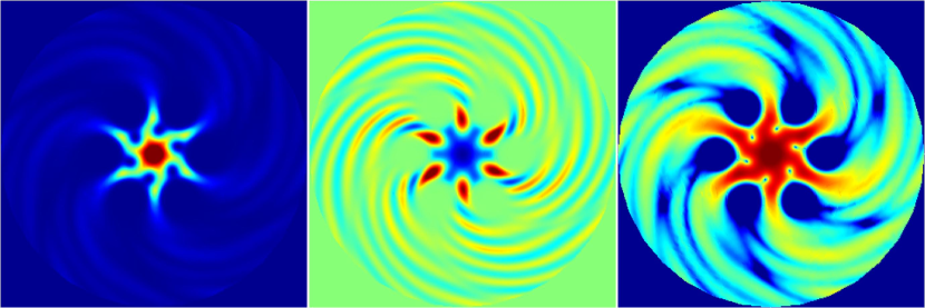
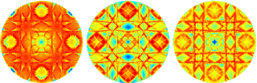
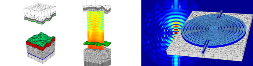
This section summarizes recent applications of our FEM implementation to simulation tasks in nanooptics. Results have been obtained in different academic and industrial research groups and collaborations, worldwide. Figures 1, 2, 3 show some exemplary applications: Specific properties of a field distribution of a guided mode in a twisted photonic crystal fiber [16, 17] are visualized in Figure 1, c.f., Section 3.3. Angular emission spectra of light emitting diode with a nano-structured cathode [18] are displayed in Figure 2, c.f., Section 3.4. Geometry discretizations and field distributions from solar cell optimization and for an integrated optical resonator are shown in Figure 3: c.f., Section 3.5 for solar cells [19], c.f., Section 3.8 for Silicon optics simulations [20].
3.1 Optical metamaterials
Optical metamaterials are nano-structured materials which can exhibit non-intuitive optical properties, like, e.g., a negative refractive index [21]. In this context, the JCMsuite FEM solver is used to investigate metamaterial building blocks like split-ring resonators with resonances at visible frequencies [22, 23], magnetic metamaterial properties[24, 25, 26, 27], refractive index properties [28], specific resonance properties [29, 30, 16], and other effects.
3.2 Plasmonics
Plasmonics, or nanoplasmonics, is the general field of optical phenomena related to the electromagnetic response of metals [2]. This includes typical optical metamaterial phenomena, as summarized in the previous Section 3.1. However, in the field of plasmonics typically resonances near metal surfaces are the main focus of investigation. The sub-wavelength localization of these resonances gives rise to new physical effects and applications. Examples are nanoscale lasers and optical sensing at sub-wavelength resolution. In this context, JCMsuite is used to investigate new physical effects [31, 32, 33, 30, 34], to design plasmonic devices [35, 36, 37, 38, 39, 40, 41, 42, 43, 44, 45, 46, 47, 48, 49, 50] and to test theoretical approaches [51, 52, 53, 54].
3.3 Photonic crystal fibers
Photonic crystal fibers (PCF) [55], or more generally microstructured fibers, are a class of optical fibers with specific guiding properties which can be engineered by defining the fiber cross section geometry and the used optical materials. This enables a variety of scientific and industrial fields, e.g., frequency-comb-generation, supercontinuum-generation, guidance of ultrashort pulses, advanced fiber lasers, and others. In this field, JCMsuite is used to investigate new physical effects in PCFs [56, 32, 57, 58, 16, 17], to design PCF for specific functionalities [59, 60, 61, 62, 63, 64, 65, 66, 67, 68, 69, 70], and for further applications.
3.4 Light emitting devices
Laser diodes and light emitting diodes rely on light emission in the p-n junction of a semiconductor diode, excited by an electric current. Applications range from miniaturized light sources to energy-efficient lighting. In this field, JCMsuite is used to investigate and design optical properties of vertical cavity surface emitting lasers (VCSEL) [71], light emitting diodes (LED, OLED) [72, 18], edge emitters [73, 74, 75], plasmon lasers [39, 40], and other concepts [76, 77, 78, 79, 80, 68, 81]. In the case of high-power devices, analysis should also include thermo-optical effects [71, 82, 75].
3.5 Solar cells
Solar cells can convert light to electrical energy. For large-scale electrical power generation, thin-film solar cells are advantageous. Microstructures in the different layers of these devices are used to increase light conversion efficiency. Different concepts for so-called light-trapping rely on regular or rough, metal or dielectric nanostructures. In this field, JCMsuite is used to design solar cells for increased conversion efficiency, e.g., by optimizing light trapping effects [38, 19, 42, 43, 44, 47, 83, 84, 85, 86].
3.6 Optical lithography
Photolithography (typically at deep ultraviolet (DUV) and extreme ultraviolet (EUV) wavelengths) is used for fabrication of patterns on a nanometer scale, with applications especially in microelectronics. The field of numerical simulations in this engineering- and research-area is termed Computational lithography [87]. Numerically optimized resolution enhancement techniques (RET), optical proximity correction (OPC), and source mask optimization (SMO) help to push the resolution limits of nanofabrication further towards smaller structures. The technological framework of this field translates to challenging requirements on numerical accuracy and computation time. In this field, JCMsuite is used in various industrial collaborations [88, 89, 90, 91, 92, 93, 94, 95].
3.7 Optical metrology
In optical metrology of nanostructures accurate simulation of light propagation is an essential component [96]. A challenge consists in reducing computation times for simulation results matching predefined accuracy requirements such that the inverse problems arizing in metrological measurements can be solved online. This is especially important when real-world structures of complex geometry are considered, as it is the case in process control and characterization. In this field JCMsuite is mainly used in projects regarding optical metrology of nanostructures of interest to the semiconductor industry [97, 98, 99, 100, 101, 102, 94, 103, 104, 105, 106, 107, 108]. The FEM implementation is also used by national metrology institutes (PTB, NIST) for critical dimension metrology and other purposes [99, 101, 105, 109].
3.8 Integrated optics
Integrated optical devices (integrated optical circuits, Si-optics devices) integrate several photonic functions into one element. This allows for decreasing footprints and in principle for higher performance of standard optical components, e.g., in optical telecommunications, and for new functionalities, e.g., for sensing (so called lab-on-a-chip devices). In this field JCMsuite is mainly used to investigate devices like high-Q resonators, waveguide couplers, splitters, or add-drop filters [20, 110, 111, 112, 113].
3.9 Photonic crystals
Photonic crystals are materials with periodic arrangements of the refractive index. The specific (periodic or quasi-periodic) arrangements can lead to special properties like the opening of photonic band-gaps. Photonic-crystal fibers (see Section 3.3) are a sub-class of photonic bandgap materials. Apart from applications to PCF, in this field JCMsuite is used to investigate properties of photonic bandgap material and devices composed of photonic crystals [114, 115, 20, 110, 111, 113].
4 Conclusion
Adaptive finite-elements prove to be a versatile method for generating accurate results to state-of-the-art simulation challenges in nanooptics. We have summarized results on analysis, design and optimization of nano-structured materials and devices, ranging from fundamental research topics like metamaterials and plasmonics to industrial nanooptic applications like microlithography, photonic crystal fibers and solar cells.
Acknowledgments
This work is supported by BMBF within project Mosaic (FKZ 13N12438), by
Deutsche Forschungsgemeinschaft within DFG research center Matheon, and by the European Union
within EMRP Joint Research Project Ind 17 Scatterometry.
![[Uncaptioned image]](/html/1304.4356/assets/x4.png)
![[Uncaptioned image]](/html/1304.4356/assets/x5.png)
References
- [1] P. Monk, Finite Element Methods for Maxwell’s Equations, Oxford University Press, New York, 2003.
- [2] L. Novotny and B. Hecht, Principles of Nano-Optics, Cambridge University Press, Cambridge, UK, 2006.
- [3] J. Pomplun, S. Burger, L. Zschiedrich, and F. Schmidt, “Adaptive finite element method for simulation of optical nano structures,” phys. stat. sol. (b) 244, p. 3419, 2007.
- [4] S. Burger, J. Pomplun, and F. Schmidt, “Finite element methods for computational nano-optics,” in Encyclopedia of Nanotechnology, B. Bhushan, ed., pp. 837–843, Springer Netherlands, 2012.
- [5] L. Zschiedrich, S. Burger, R. Klose, A. Schädle, and F. Schmidt, “JCMmode: an adaptive finite element solver for the computation of leaky modes,” Proc. SPIE 5728, p. 192, 2005.
- [6] S. Burger, L. Zschiedrich, J. Pomplun, and F. Schmidt, “JCMsuite: An adaptive FEM solver for precise simulations in nano-optics,” in Integrated Photonics and Nanophotonics Research and Applications, p. ITuE4, Optical Society of America, 2008.
- [7] T. Hohage, F. Schmidt, and L. Zschiedrich, “Solving Time-Harmonic Scattering Problems Based on the Pole ConditionII: Convergence of the PML Method,” SIAM J. Math. Anal. 35, p. 547, 2003.
- [8] L. Zschiedrich, R. Klose, A. Schädle, and F. Schmidt, “A new finite element realization of the Perfectly Matched Layer Method for Helmholtz scattering problems on polygonal domains in 2D,” J. Comput. Appl. Math. 188, p. 12, 2006.
- [9] L. Zschiedrich, S. Burger, B. Kettner, and F. Schmidt, “Advanced finite element method for nano-resonators,” Proc. SPIE 6115, p. 611515, 2006.
- [10] L. Zschiedrich, S. Burger, A. Schädle, and F. Schmidt, “Domain decomposition method for electromagnetic scattering problems,” in Proceedings of the 5th International Conference on Numerical Simulation of Optoelectronic devices, p. 55, 2005.
- [11] A. Schädle, L. Zschiedrich, S. Burger, R. Klose, and F. Schmidt, “Domain decomposition method for maxwell’s equations: Scattering off periodic structures,” J. Comp. Phys. 226, p. 447, 2007.
- [12] L. Zschiedrich, S. Burger, A. Schädle, and F. Schmidt, “A rigorous finite-element domain decomposition method for electromagnetic near field simulations,” Proc. SPIE 6924, p. 692450, 2008.
- [13] J. Pomplun and F. Schmidt, “Reduced basis method for electromagnetic field computations,” in Scientific Computing in Electrical Engineering SCEE 2008, p. 85, Springer Berlin Heidelberg, 2010.
- [14] J. Pomplun and F. Schmidt, “Accelerated a posteriori error estimation for the reduced basis method with application to 3D electromagnetic scattering problems,” SIAM Journal on Scientific Computing 32, p. 498, 2010.
- [15] L. Zschiedrich, S. Burger, J. Pomplun, and F. Schmidt, “Goal oriented adaptive finite element method for the precise simulation of optical components,” Proc. SPIE 6475, p. 64750H, 2007.
- [16] G. Wong, M. Kang, H. Lee, S. Burger, L. Zschiedrich, F. Biancalana, and Russell, P.J.St., “Strongly twisted solid-core PCF: A one-dimensional chiral metamaterial,” in Frontiers in Optics, Optical Society of America, 2011.
- [17] G. Wong, M. Kang, H. Lee, F. Biancalana, C. Conti, T. Weiss, and P. S. J. Russell, “Excitation of orbital angular momentum resonances in helically twisted photonic crystal fiber,” Science 337, p. 446, 2012.
- [18] L. Zschiedrich, H. J. Greiner, S. Burger, and F. Schmidt, “Numerical analysis of nanostructures for enhanced light extraction from OLEDs,” Proc. SPIE 8641, 2013.
- [19] D. Lockau, L. Zschiedrich, S. Burger, F. Schmidt, F. Ruske, and B. Rech, “Rigorous optical simulation of light management in crystalline silicon thin film solar cells with rough interface textures,” Proc. SPIE 7933, p. 79330M, 2011.
- [20] S. Burger, F. Schmidt, and L. Zschiedrich, “Numerical investigation of optical resonances in circular grating resonators,” Proc. SPIE 7606, p. 760610, 2010.
- [21] W. Cai and V. Shalaev, Optical Metamaterials: Fundamentals and Applications, Springer, 2009.
- [22] C. Enkrich, M. Wegener, S. Linden, S. Burger, L. Zschiedrich, F. Schmidt, C. Zhou, T. Koschny, and C. M. Soukoulis, “Magnetic metamaterials at telecommunication and visible frequencies,” Phys. Rev. Lett. 95, p. 203901, 2005.
- [23] S. Burger, L. Zschiedrich, R. Klose, A. Schädle, F. Schmidt, C. Enkrich, S. Linden, M. Wegener, and C. M. Soukoulis, “Numerical investigation of light scattering off split-ring resonators,” Proc. SPIE 5955, p. 595503, 2005.
- [24] G. Dolling, M. Wegener, A. Schädle, S. Burger, and S. Linden, “Observation of magnetization waves in negative-index photonic metamaterials,” Appl. Phys. Lett. 89, p. 231118, 2006.
- [25] S. Linden, C. Enkrich, G. Dolling, M. W. Klein, J. Zhou, T. Koschny, C. M. Soukoulis, S. Burger, F. Schmidt, and M. Wegener, “Photonic metamaterials: Magnetism at optical frequencies,” IEEE Journal of Selected Topics in Quantum Electronics 12, p. 1097, 2006.
- [26] M. Decker, S. Burger, S. Linden, and M. Wegener, “Magnetization waves in split-ring-resonator arrays: Evidence for retardation effects,” Phys. Rev. B 80, p. 193102, 2009.
- [27] K. Tsakmakidis, M. Wartak, J. Cook, J. Hamm, and O. Hess, “Negative-permeability electromagnetically induced transparent and magnetically active metamaterials,” Physical Review B 81, p. 195128, 2010.
- [28] G. Dolling, M. W. Klein, M. Wegener, A. Schädle, B.Kettner, S. Burger, and S. Linden, “Negative beam displacement for negative-index photonic metamaterials,” Optics Express 15, p. 14219, 2007.
- [29] J. K. Gansel, M. Wegener, S. Burger, and S. Linden, “Gold helix photonic metamaterials: A numerical parameter study,” Opt. Express 18, p. 1059, 2010.
- [30] J. Zhao, B. Frank, S. Burger, and H. Giessen, “Large-area high-quality plasmonic oligomers fabricated by angle-controlled colloidal nanolithography,” ACS Nano 5, p. 9009, 2011.
- [31] T. Kalkbrenner, U. Hakanson, A. Schädle, S. Burger, C. Henkel, and V. Sandoghdar, “Optical microscopy using the spectral modifications of a nano-antenna,” Phys. Rev. Lett. 95, p. 200801, 2005.
- [32] H. Lee, M. Schmidt, H. Tyagi, L. P. Sempere, and P. S. J. Russell, “Polarization-dependent coupling to plasmon modes on submicron gold wire in photonic crystal fiber,” Applied Physics Letters 93, p. 111102, 2008.
- [33] S. Burger, B. H. Kleemann, L. Zschiedrich, and F. Schmidt, “Finite-element simulations of light propagation through circular subwavelength apertures,” Proc. SPIE 7366, p. 736621, 2009.
- [34] H. Lee, M. Schmidt, and P. S. J. Russell, “Excitation of a nanowire “molecule” in gold-filled photonic crystal fiber,” Optics Letters 37, p. 2946, 2012.
- [35] A. Unger, U. Rietzler, R. Berger, and M. Kreiter, “Sensitivity of crescent-shaped metal nanoparticles to attachment of dielectric colloids,” Nano Letters 9, p. 2311, 2009.
- [36] M. F. Klein, H. Hein, P.-J. Jakobs, S. Linden, N. Meinzer, M. Wegener, V. Saile, and M. Kohl, “Electron beam lithography of v-shaped silver nanoantennas,” Microelectronic Engineering 86, p. 1078, 2009.
- [37] D. Lockau, L. Zschiedrich, and S. Burger, “Accurate simulation of light transmission through subwavelength apertures in metal films,” J. Opt. A: Pure Appl. Opt. 11, p. 114013, 2009.
- [38] D. Lockau, L. Zschiedrich, F. Schmidt, S. Burger, and B. Rech, “Efficient simulation of plasmonic structures for solar cells,” in International Workshop on Optical Waveguide Theory and Numerical Modelling, XVIII, p. 48, Fraunhofer Institute IOF, 2009.
- [39] S. Burger, L. Zschiedrich, J. Pomplun, and F. Schmidt, “Finite element method for accurate 3d simulation of plasmonic waveguides,” Proc. SPIE 7604, p. 76040F, 2010.
- [40] S. Burger, L. Zschiedrich, and F. Schmidt, “FEM simulation of plasmon laser resonances,” AIP Conf. Proc. 1281, p. 1613, 2010.
- [41] R. Mohammadi, A. Unger, H. Elmers, G. Schönhense, M. Shushtari, and M. Kreiter, “Manipulating near field polarization beyond the diffraction limit,” Applied Physics B: Lasers and Optics 104, p. 65, 2011.
- [42] T. Benkenstein, M. Flämmich, T. Harzendorf, T. Käsebier, D. Michaelis, M. Oliva, C. Wächter, and U. Zeitner, “Effects of metallic nanoparticle arrays in si solar cell structures,” Proc. SPIE 8110, p. 81100D, 2011.
- [43] U. W. Paetzold, E. Moulin, B. E. Pieters, R. Carius, and U. Rau, “Design of nanostructured plasmonic back contacts for thin-film silicon solar cells,” Optics Express 19, p. A1219, 2011.
- [44] U. Paetzold, E. Moulin, D. Michaelis, W. Bottler, C. Wachter, V. Hagemann, M. Meier, R. Carius, and U. Rau, “Plasmonic reflection grating back contacts for microcrystalline silicon solar cells,” Applied Physics Letters 99, p. 181105, 2011.
- [45] J. Fischer, N. Vogel, R. Mohammadi, H.-J. Butt, K. Landfester, C. K. Weiss, and M. Kreiter, “Plasmon hybridization and strong near-field enhancements in opposing nanocrescent dimers with tunable resonances,” Nanoscale 3, p. 4788, 2011.
- [46] A. Husakou, F. Kelkensberg, J. Herrmann, and M. Vrakking, “Polarization gating and circularly-polarized high harmonic generation using plasmonic enhancement in metal nanostructures,” Optics Express 19, p. 25346, 2011.
- [47] U. W. Paetzold, M. Meier, E. Moulin, V. Smirnov, B. E. Pieters, U. Rau, and R. Carius, “Plasmonic back contacts with non-ordered Ag nanostructures for light trapping in thin-film silicon solar cells,” Materials Science and Engineering: B , p. DOI: 10.1016/j.mseb.2012.10.013, 2012.
- [48] M. Richter, F. Schlosser, M. Schoth, S. Burger, F. Schmidt, A. Knorr, and S. Mukamel, “Reconstruction of the wave functions of coupled nanoscopic emitters using a coherent optical technique,” Phys. Rev. B 86, p. 085308, 2012.
- [49] G. Kewes, A. W. Schell, R. Henze, R. S. Schonfeld, S. Burger, K. Busch, and O. Benson, “Design and numerical optimization of an easy-to-fabricate photon-to-plasmon coupler for quantum plasmonics,” Applied Physics Letters 102, p. 051104, 2013.
- [50] H.-D. Yan, P. Lemmens, J. Ahrens, M. Bröring, S. Burger, W. Daum, G. Lilienkamp, S. Korte, A. Lak, and M. Schilling, “High-density array of au nanowires coupled by plasmon modes,” Acta Phys. Sin. 61, p. 237106, 2012.
- [51] J. Hoffmann, C. Hafner, P. Leidenberger, J. Hesselbarth, and S. Burger, “Comparison of electromagnetic field solvers for the 3D analysis of plasmonic nano antennas,” Proc. SPIE 7390, p. 73900J, 2009.
- [52] A. Husakou, S.-J. Im, and J. Herrmann, “Theory of plasmon-enhanced high-order harmonic generation in the vicinity of metal nanostructures in noble gases,” Physical Review A 83, p. 043839, 2011.
- [53] V. E. Babicheva, S. S. Vergeles, P. E. Vorobev, and S. Burger, “Localized surface plasmon modes in a system of two interacting metallic cylinders,” J. Opt. Soc. Am. B 29, p. 1263, 2012.
- [54] K. R. Hiremath, L. Zschiedrich, and F. Schmidt, “Numerical solution of nonlocal hydrodynamic Drude model for arbitrary shaped nano-plasmonic structures using Nedelec finite elements,” Journal of Computational Physics 231, p. 5890, 2012.
- [55] P. Russell, “Photonic crystal fibers,” Science 299, p. 358, 2003.
- [56] G. J. Pearce, G. S. Wiederhecker, C. G. Poulton, S. Burger, and P. S. J. Russell, “Models for guidance in kagome-structured hollow-core photonic crystal fibres,” Optics Express 15, p. 12680, 2007.
- [57] H. Tyagi, M. Schmidt, L. Prill Sempere, and P. Russell, “Optical properties of photonic crystal fiber with integral micron-sized ge wire,” Optics Express 16, p. 17227, 2008.
- [58] J. C. Travers, W. Chang, J. Nold, N. Y. Joly, and P. S. J. Russell, “Ultrafast nonlinear optics in gas-filled hollow-core photonic crystal fibers [invited],” JOSA B 28, p. A11, 2011.
- [59] R. Holzlöhner, S. Burger, P. J. Roberts, and J. Pomplun, “Efficient optimization of hollow-core photonic crystal fiber design using the finite-element method,” J. Europ. Opt. Soc: Rap. Comm. 1, p. 06011, 2006.
- [60] F. Couny, F. Benabid, P. Roberts, P. Light, and M. Raymer, “Generation and photonic guidance of multi-octave optical-frequency combs,” Science 318, p. 1118, 2007.
- [61] J. Pomplun, L. Zschiedrich, R. Klose, F. Schmidt, and S. Burger, “Finite element simulation of radiation losses in photonic crystal fibers,” phys. stat. sol. (a) 204, p. 3822, 2007.
- [62] J. Lægsgaard and P. J. Roberts, “Dispersive pulse compression in hollow-core photonic bandgap fibers,” Optics Express 16, p. 9628, 2008.
- [63] J. Bethge, G. Steinmeyer, S. Burger, F. Lederer, and R. Iliew, “Guiding properties of chirped photonic crystal fibers,” J. Lightwave Technology 27, p. 1698, 2009.
- [64] S.-J. Im, A. Husakou, and J. Herrmann, “Guiding properties and dispersion control of kagome lattice hollow-core photonic crystal fibers,” Optics Express 17, p. 13050, 2009.
- [65] J. Nold, P. Hölzer, N. Joly, G. Wong, A. Nazarkin, A. Podlipensky, M. Scharrer, and P. S. J. Russell, “Pressure-controlled phase matching to third harmonic in ar-filled hollow-core photonic crystal fiber,” Optics Letters 35, p. 2922, 2010.
- [66] J. Weirich, J. Lægsgaard, L. Wei, T. T. Alkeskjold, T. X. Wu, S.-T. Wu, and A. Bjarklev, “Liquid crystal parameter analysis for tunable photonic bandgap fiber devices,” Optics Express 18, p. 4074, 2010.
- [67] Y. Wang, N. V. Wheeler, F. Couny, P. Roberts, and F. Benabid, “Low loss broadband transmission in hypocycloid-core Kagome hollow-core photonic crystal fiber,” Optics Letters 36, p. 669, 2011.
- [68] A. M. Jones, A. Nampoothiri, A. Ratanavis, T. Fiedler, N. V. Wheeler, F. Couny, R. Kadel, F. Benabid, B. R. Washburn, K. L. Corwin, et al., “Mid-infrared gas filled photonic crystal fiber laser based on population inversion,” Optics Express 19, p. 2309, 2011.
- [69] M. Laurila, T. T. Alkeskjold, J. Laegsgaard, and J. Broeng, “Spatial and spectral imaging of LMA photonic crystal fiber amplifiers,” Proc. SPIE 7914, p. 79142D, 2011.
- [70] M. Laurila, T. T. Alkeskjold, J. Lægsgaard, and J. Broeng, “Modal analysis of a large-mode area photonic crystal fiber amplifier using spectral-resolved imaging,” Optical Engineering 50, p. 111604, 2011.
- [71] M. Rozova, J. Pomplun, L. Zschiedrich, F. Schmidt, and S. Burger, “3D finite element simulation of optical modes in VCSELs,” Proc. SPIE 8255, p. 82550K, 2012.
- [72] L. Zschiedrich, H. Greiner, J. Pomplun, M. Hammerschmidt, S. Burger, and F. Schmidt, “FEM simulations of light extraction from nanostructured organic light-emitting diodes,” in Renewable Energy and the Environment Optics and Photonics Congress, Renewable Energy and the Environment Optics and Photonics Congress , p. LT2B.5, Optical Society of America, 2012.
- [73] J. Pomplun, S. Burger, F. Schmidt, A. Schliwa, D. Bimberg, A. Pietrzak, H. Wenzel, and G. Erbert, “Finite element simulation of the optical modes of semiconductor lasers,” phys. stat. sol. (b) 247, p. 846, 2010.
- [74] H. Wenzel, P. Crump, H. Ekhteraei, C. Schultz, J. Pomplun, S. Burger, L. Zschiedrich, F. Schmidt, and G. Erbert, “Theoretical and experimental analysis of the lateral modes of high-power broad-area lasers,” in Numerical Simulation of Optoelectronic Devices (NUSOD), 2011 11th International Conference on, p. 143, IEEE, 2011.
- [75] H. Wenzel, “Basic aspects of high-power semiconductor laser simulation,” arXiv preprint arXiv:1302.0173 , 2013.
- [76] M. Karl, B. Kettner, S. Burger, F. Schmidt, H. Kalt, and M. Hetterich, “Dependencies of micro-pillar cavity quality factors calculated with finite element methods,” Optics Express 17, p. 1144, 2009.
- [77] T. Grossmann, S. Schleede, M. Hauser, M. B. Christiansen, C. Vannahme, C. Eschenbaum, S. Klinkhammer, T. Beck, J. Fuchs, G. U. Nienhaus, et al., “Low-threshold conical microcavity dye lasers,” Applied Physics Letters 97, p. 063304, 2010.
- [78] T. Grossmann, M. Hauser, T. Beck, C. Gohn-Kreuz, M. Karl, H. Kalt, C. Vannahme, and T. Mappes, “High-Q conical polymeric microcavities,” Applied Physics Letters 96, p. 013303, 2010.
- [79] T. Grossmann, S. Klinkhammer, M. Hauser, D. Floess, T. Beck, C. Vannahme, T. Mappes, U. Lemmer, and H. Kalt, “Strongly confined, low-threshold laser modes in organic semiconductor microgoblets,” Optics Express 19, p. 10009, 2011.
- [80] M. Karl, D. Rülke, T. Beck, D. Hu, D. Schaadt, H. Kalt, and M. Hetterich, “Reversed pyramids as novel optical micro-cavities,” Superlattices and Microstructures 47, p. 83, 2010.
- [81] T. Beck, M. Hauser, T. Grossmann, D. Floess, S. Schleede, J. Fischer, C. Vannahme, T. Mappes, and H. Kalt, “PMMA-micro goblet resonators for biosensing applications,” Proc. SPIE 7888, p. 78880A, 2011.
- [82] J. Pomplun, H. Wenzel, S. Burger, L. Zschiedrich, M. Rozova, F. Schmidt, P. Crump, H. Ekhteraei, C. M. Schultz, and G. Erbert, “Thermo-optical simulation of high-power diode lasers,” Proc. SPIE 8255, p. 825510, 2012.
- [83] M. Blome, K. McPeak, S. Burger, F. Schmidt, and D. Norris, “Back-reflector optimization in thin-film silicon solar cells using 3D finite element simulations,” in Int. Conf. on Scientific Computing in Electrical Engineering (SCEE), 2012.
- [84] C. Becker, D. Lockau, T. Sontheimer, P. Schubert-Bischoff, E. Rudigier-Voigt, M. Bockmeyer, F. Schmidt, and B. Rech, “Large-area 2d periodic crystalline silicon nanodome arrays on nanoimprinted glass exhibiting photonic band structure effects,” Nanotechnology 23, p. 135302, 2012.
- [85] D. Lockau, T. Sontheimer, C. Becker, E. Rudigier-Voigt, F. Schmidt, and B. Rech, “Nanophotonic light trapping in 3-dimensional thin-film silicon architectures,” Optics Express 21, p. A42, 2013.
- [86] M. Hammerschmidt, D. Lockau, S. Burger, F. Schmidt, C. Schwanke, S. Kirner, S. Calnan, B. Stannowski, and B. Rech, “3D optical modeling of thin-film a-Si/c-Si tandem solar cells with random textured interfaces using FEM,” in Optical Instrumentation for Energy and Environmental Applications, Optical Society of America, 2012.
- [87] K. Lai, “Review of computational lithography modeling: focusing on extending optical lithography and design-technology co-optimization,” Adv. Opt. Techn. 1, p. 249, 2012.
- [88] S. Burger, R. Köhle, L. Zschiedrich, W. Gao, F. Schmidt, R. März, and C. Nölscher, “Benchmark of FEM, waveguide and FDTD algorithms for rigorous mask simulation,” Proc. SPIE 5992, p. 599216, 2005.
- [89] S. Burger, R. Köhle, L. Zschiedrich, H. Nguyen, F. Schmidt, R. März, and C. Nölscher, “Rigorous simulation of 3D masks,” Proc. SPIE 6349, p. 63494Z, 2006.
- [90] S. Burger, L. Zschiedrich, F. Schmidt, R. Köhle, B. Küchler, and C. Nölscher, “EMF simulations of isolated and periodic 3D photomask patterns,” Proc. SPIE 6730, p. 67301W, 2007.
- [91] Y. Tezuka, J. Cullins, Y. Tanaka, T. Hashimoto, I. Nishiyama, and T. Shoki, “EUV exposure experiment using programmed multilayer defects for refining printability simulation,” Proc. SPIE 6517, p. 65172M, 2007.
- [92] S. Burger, L. Zschiedrich, F. Schmidt, P. Evanschitzky, and A. Erdmann, “Benchmark of rigorous methods for electromagnetic field simulation,” Proc. SPIE 7122, p. 71221S, 2008.
- [93] J. Pomplun, L. Zschiedrich, S. Burger, F. Schmidt, J. Tyminski, D. Flagello, and N. Toshiharu, “Reduced basis method for source mask optimization,” Proc. SPIE 7823, p. 78230E, 2010.
- [94] S. Burger, L. Zschiedrich, J. Pomplun, and F. Schmidt, “Rigorous simulations of 3D patterns on extreme ultraviolet lithography masks,” Proc. SPIE 8083, p. 80831B, 2011.
- [95] J. K. Tyminski, R. Popescu, S. Burger, J. Pomplun, L. Zschiedrich, T. Matsuyama, and T. Noda, “Finite element models of lithographic mask topography,” Proc. SPIE 8326, p. 83261B, 2012.
- [96] L. Pang, D. Peng, P. Hu, D. Chen, L. He, Y. Li, M. Satake, and V. Tolani, “Computational metrology and inspection (CMI) in mask inspection, metrology, review, and repair,” Adv. Opt. Techn. 1, p. 299, 2012.
- [97] F. Scholze, C. Laubis, U. Dersch, J. Pomplun, S. Burger, and F. Schmidt, “The influence of line edge roughness and CD uniformity on EUV scatterometry for CD characterization of EUV masks,” Proc. SPIE 6617, p. 66171A, 2007.
- [98] F. Scholze, C. Laubis, G. Ulm, U. Dersch, J. Pomplun, S. Burger, and F. Schmidt, “Evaluation of EUV scatterometry for CD characterization of EUV masks using rigorous FEM-simulation,” Proc. SPIE 6921, p. 69213R, 2008.
- [99] J. Potzick, R. Dixson, R. Quintanilha, M. Stocker, A. Vladar, E. Buhr, W. Häßler-Grohne, B. Bodermann, C. Frase, and H. Bosse, “International photomask linewidth comparison by NIST and PTB,” Proc. SPIE 7122, p. 71222P, 2008.
- [100] J. Pomplun, S. Burger, F. Schmidt, F. Scholze, C. Laubis, and U. Dersch, “Metrology of EUV masks by EUV-scatterometry and finite element analysis,” Proc. SPIE 7028, p. 70280P, 2008.
- [101] R. Quintanilha, Y. Sohn, B. Barnes, L. Howard, and R. Silver, “Critical dimension measurements using a 193 nm scatterfield microscope,” Proc. SPIE 7390, p. 73900S, 2009.
- [102] J. Pomplun, L. Zschiedrich, S. Burger, and F. Schmidt, “Reduced basis method for computational lithography,” Proc. SPIE 7488, p. 74882B, 2009.
- [103] S. Burger, L. Zschiedrich, J. Pomplun, F. Schmidt, A. Kato, C. Laubis, and F. Scholze, “Investigation of 3D patterns on EUV masks by means of scatterometry and comparison to numerical simulations,” Proc. SPIE 8166, p. 81661Q, 2011.
- [104] B. Bodermann, E. Buhr, H.-U. Danzebrink, M. Bär, F. Scholze, M. Krumrey, M. Wurm, P. Klapetek, P.-E. Hansen, V. Korpelainen, M. van Veghel, A. Yacoot, S. Siitonen, O. E. Gawhary, S. Burger, and T. Saastamoinen, “Joint research on scatterometry and AFM wafer metrology,” AIP Conference Proceedings 1395, p. 319, 2011.
- [105] B. Bodermann, P.-E. Hansen, S. Burger, M.-A. Henn, H. A. Gross, M. Bär, F. Scholze, J. Endres, and M. Wurm, “First steps towards a scatterometry reference standard,” Proc. SPIE 8466, p. 84660E, 2012.
- [106] B. H. Kleemann, J. Kurz, J. Hetzler, J. Pomplun, S. Burger, L. Zschiedrich, and F. Schmidt, “Fast online inverse scattering with Reduced Basis Method (RBM) for a 3D phase grating with specific line roughness,” Proc. SPIE 8083, p. 808309, 2011.
- [107] A. Kato, S. Burger, and F. Scholze, “Analytical modeling and 3D finite element simulation of line edge roughness in scatterometry,” Appl. Optics 51, p. 6457, 2012.
- [108] L. Zang, T. Euser, M. Kang, M. Scharrer, and P. S. J. Russell, “Structural analysis of photonic crystal fibers by side scattering of laser light,” Optics Letters 36(9), p. 1668, 2011.
- [109] B. Bodermann, E. Buhr, Z. Li, and H. Bosse, “Quantitative optical microscopy at the nanoscale: New developments and comparisons,” Optical Imaging and Metrology , 2012.
- [110] S. Burger, F. Schmidt, and L. Zschiedrich, “Numerical investigation of photonic crystal microcavities in silicon-on-insulator waveguides,” Proc. SPIE 7609, p. 76091Q, 2010.
- [111] S. Burger, J. Pomplun, F. Schmidt, and L. Zschiedrich, “Finite-element method simulations of high-Q nanocavities with 1D photonic bandgap,” Proc. SPIE 7933, p. 79330T, 2011.
- [112] S. Warm, A. A. Juarez, B. Wohlfeil, and K. Petermann, “Cross-talk in mode-division-multiplex optical fiber transmission systems,” in Transparent Optical Networks (ICTON), 2011 13th International Conference on, IEEE, 2011.
- [113] J. Petracek, B. Maes, S. Burger, J. Luksch, P. Kwiecien, and I. Richter, “Simulation of high-Q nanocavities with 1D photonic gap,” in Transparent Optical Networks (ICTON), IEEE, 2012.
- [114] Y. Neve-Oz, T. Pollok, S. Burger, M. Golosovsky, and D. Davidov, “Resonant transmission of electromagnetic waves through 2d photonic quasicrystals,” J. Appl. Phys. 107, p. 063105, 2010.
- [115] S. Burger, R. Klose, A. Schädle, F. Schmidt, and L. Zschiedrich, “FEM modelling of 3d photonic crystals and photonic crystal waveguides,” Proc. SPIE 5728, p. 164, 2005.