Single-hole tunneling through a two-dimensional hole gas in intrinsic silicon.
Abstract
In this letter we report single-hole tunneling through a quantum dot in a two-dimensional hole gas, situated in a narrow-channel field-effect transistor in intrinsic silicon. Two layers of aluminum gate electrodes are defined on Si/SiO2 using electron-beam lithography. Fabrication and subsequent electrical characterization of different devices yield reproducible results, such as typical MOSFET turn-on and pinch-off characteristics. Additionally, linear transport measurements at 4 K result in regularly spaced Coulomb oscillations, corresponding to single-hole tunneling through individual Coulomb islands. These Coulomb peaks are visible over a broad range in gate voltage, indicating very stable device operation. Energy spectroscopy measurements show closed Coulomb diamonds with single-hole charging energies of 5–10 meV, and lines of increased conductance as a result of resonant tunneling through additional available hole states.
In order for sufficient coherent operations to be performed in a proposed quantum computer Ladd et al. (2010), the quantum states of the corresponding qubits are required to be long-lived. In the scheme proposed by Loss and DiVincenzo (1998), quantum logic gates perform operations on coupled spin states of single electrons in neighboring quantum dots. Most experiments have focused on quantum dots formed in III-V semiconductors, especially GaAs van der Wiel et al. (2002); Hanson et al. (2007); however, electron spin coherence in those materials is limited by hyperfine interactions with nuclear spins and spin-orbit coupling. Group IV materials are believed to have long spin lifetimes because of weak spin-orbit interactions and the predominance of spin-zero nuclei. This prospect has stimulated significant experimental effort to isolate single charges in carbon nanotubes Jarillo-Herrero et al. (2004); Kuemmeth et al. (2008), Si/SiGe heterostructures Simmons et al. (2007); Borselli et al. (2011), Si nanowires Zwanenburg et al. (2009), planar Si MOS structures Lim et al. (2009), and dopants in Si Lansbergen et al. (2008); Fuechsle et al. (2012); Prati et al. (2012). Silicon not only holds promise for very long coherence times Steger et al. (2012), but also for bringing scalability of quantum devices one step closer, and has thus attracted much attention for quantum computing purposes Morton et al. (2011); Zwanenburg et al. (2012).
Recently, coherent driven oscillations of individual electron and nuclear spins in silicon were reported Pla et al. (2012, 2013). The spin resonance was magnetically driven by sending alternating currents through a nearby microwave line. A technologically more attractive way is electric-field induced electron spin resonance, as demonstrated in quantum dots made in GaAs/AlGaAs heterostructures Nowack et al. (2007); Laird et al. (2007); Pioro-Ladriere et al. (2008), InAs nanowires Nadj-Perge et al. (2010), and InSb nanowires Pribiag et al. (2013). Electrical control of single spins requires mediation by either hyperfine or spin-orbit interaction. Although the latter is too weak for electrically driven spin resonance of electrons in silicon, the spin-orbit interaction for holes may well facilitate hole spin resonance by means of electric fields.
Up until now, single-hole spins have not yet been investigated in electrostatically defined silicon quantum dots. Here, we report on single-hole tunneling (SHT) in a gated silicon MOSFET nanostructure, based on an earlier n-type design by Angus et al. (2007). In this work we focus on low-temperature transport measurements through a two-dimensional hole gas (2DHG), which is electrostatically defined by a MOSFET-type architecture. To create the 2DHG we apply a negative potential to metallic gates on top of oxidized intrinsic silicon, raising the valence band to above the Fermi energy, thus allowing states to be occupied by holes. At 4 K we observe single-hole tunneling and demonstrate control of the charge occupation in unintentionally created quantum dots. We are aware that similar results have simultaneously been obtained elsewhere Li et al. (2013).
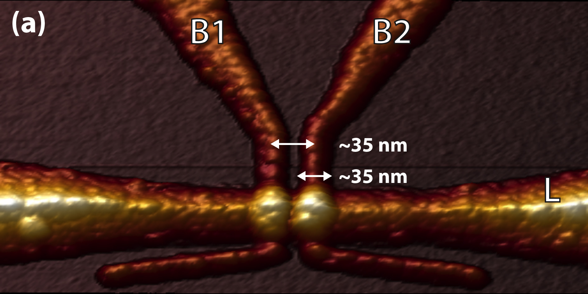
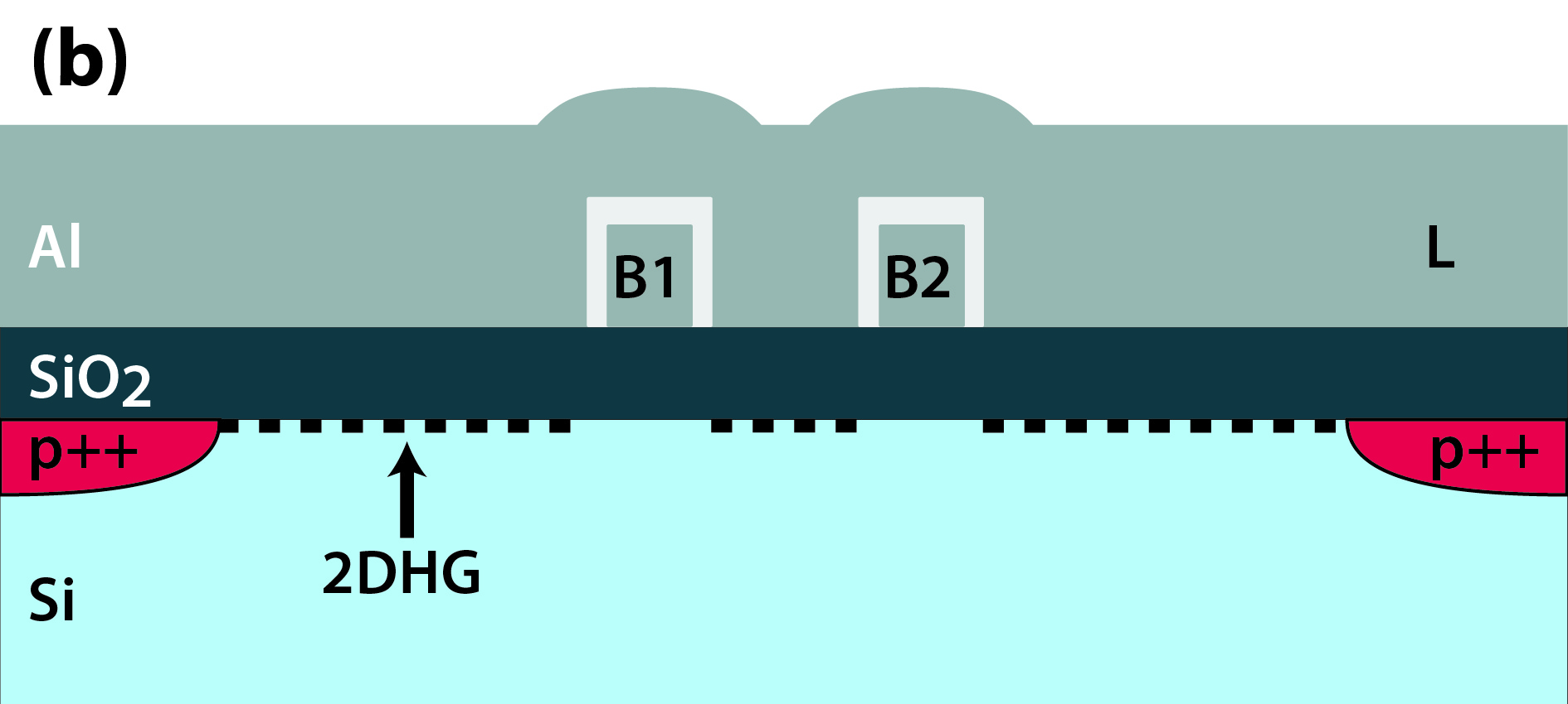
Figure 1 shows an atomic force microscope image and a schematic cross section of the device structure, made with a combination of optical and electron-beam lithography (EBL), based on the recipe as described by Angus et al. (2007). Near-intrinsic silicon () is used as the substrate. Source and drain regions are implanted with boron dopant atoms, which are activated by rapid thermal annealing, and serve as hole reservoirs. Ohmic contacts to these regions are made by sputtering Al-Si alloy (99:1) contact pads. A nm thick high-quality SiO2 oxide window is thermally grown at and serves as an insulating barrier between the substrate and the aluminum gates. To remove charge traps and defects such as dangling bonds, the oxide is annealed in pure at and a pressure of mbar. Contact pads for gates are defined using optical lithography followed by development, evaporation of Ti/Pt, and subsequent lift-off. EBL is used to define the sub-micron aluminum gates, which will electrostatically control hole accumulation. Atomic force microscopy images show barrier gates with a typical width, height, and separation of nm, see figure 1. After oxidation of the barrier gates, a second EBL step is used to define the lead gate. We have measured various devices and report here characteristic behavior of a representative sample.
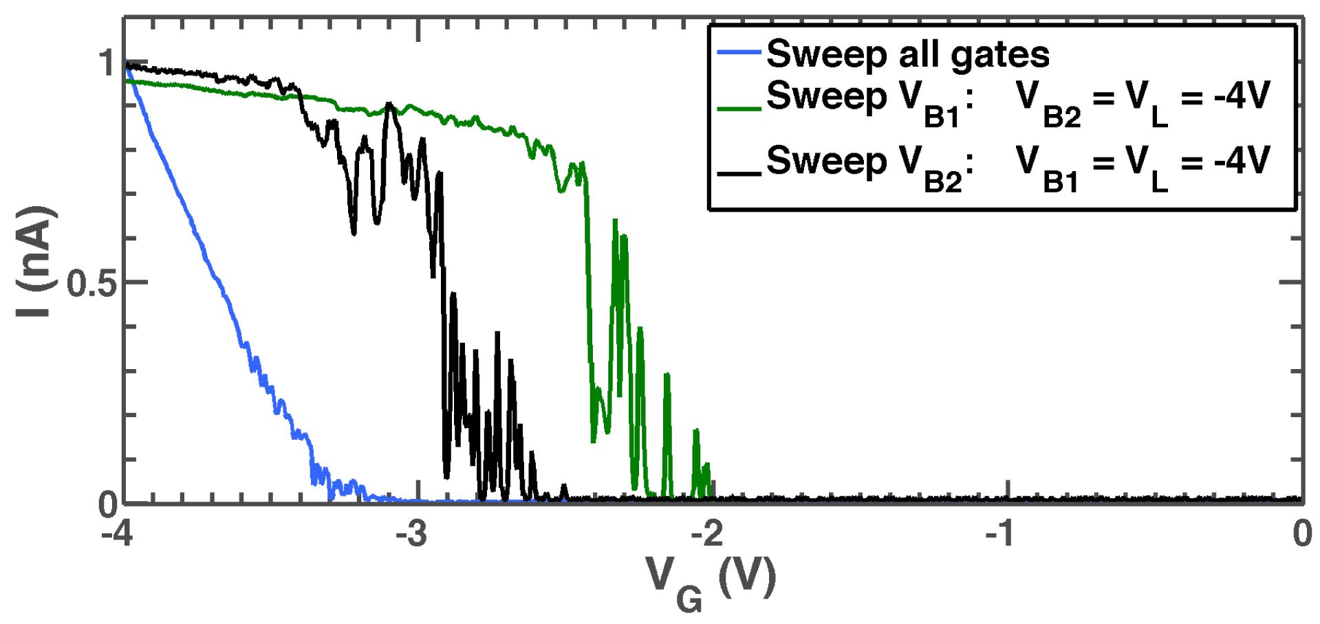
To characterize hole transport in our devices we perform electrical transport measurements on samples submerged in liquid helium at a temperature of K. Low-noise current amplifiers and voltage sources in combination with Pi-filters were used to characterize the devices. To measure a typical MOSFET turn-on characteristic, the same voltage is applied to all gates: . Simultaneously, a bias voltage is applied to the source and drain contacts. The gate voltages are then ramped to negative voltages while measuring the resulting current . Once the threshold voltage is reached, the valence band is pulled sufficiently above the Fermi energy so that hole states become available to be occupied. In the resulting 2DHG, holes can then flow from source to drain and the device is ‘turned on’. During the sweeping of the gate voltages, the current increases up to roughly 1 nA, as shown in figure 2. The ability of the barrier gates to influence conduction in the 2DHG below the barriers is critical to operation of the devices. The barrier gate voltages and should be able to tune the corresponding potential barriers from highly transparent ( nA) to opaque ( nA). To test this, a ‘pinch-off’ curve is measured, by making the voltage on a barrier less negative whilst keeping the other gates well beyond the threshold voltage. Both barriers B1 and B2 can individually pinch off the conduction channel, and additionally show some resonances in the measured current. The results in Figure 2 show the ability of each of the barriers to effectively control conduction in the channel.
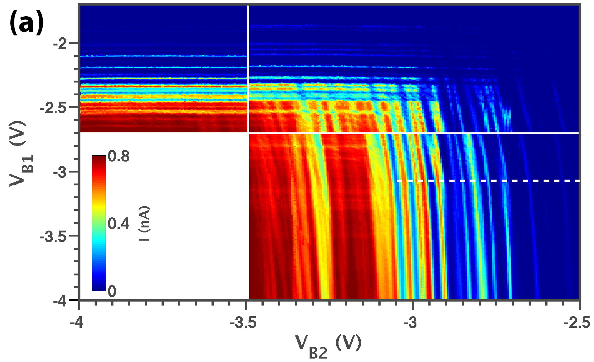
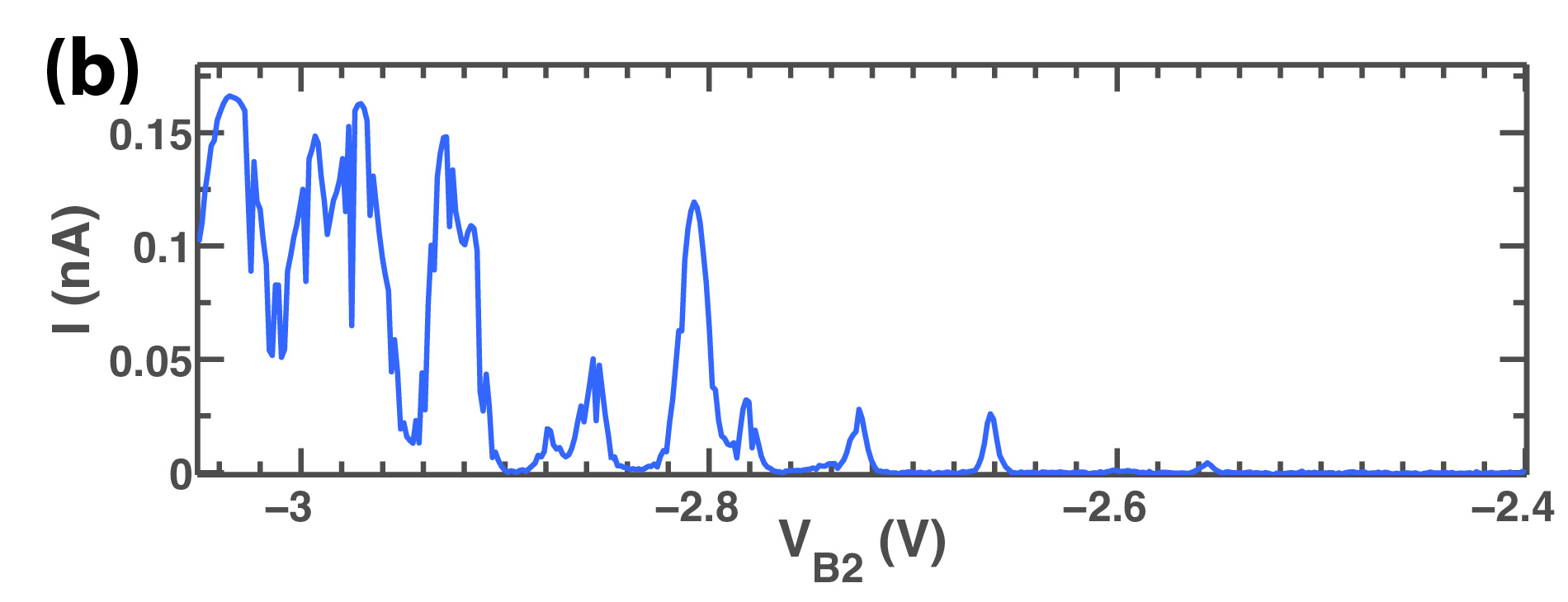
Next, we measure the current versus both barrier gate voltages at constant bias and lead gate voltage (see Figure 3). When the voltage applied to the barrier gates is too close to zero ( or ), the tunneling rate through the potential barriers becomes negligible. The current as a function of voltage applied to the barrier gates shows periodic resonances parallel to the axes of both and . Resonances parallel to the axis of () are not influenced by a change in (), indicating that those features are independently coupled to and . We now focus on one of these resonances; specifically the one coupled most strongly to B2. To probe the features of this resonance, a constant and is applied where is chosen such that the corresponding barrier is highly transparent. The subsequent measured source-drain current as a function of in figure 3 shows periodic current peaks separated by regions of zero current. The sharp peaks correspond to Coulomb oscillations with regions of Coulomb blockade in between. Each time a peak is traversed, the occupation of the corresponding Coulomb island changes by one hole in a charge transition , with the number holes on the island. We can thus control the charge occupation of individual islands below the barrier gates. These islands are likely formed by disorder or roughness, e.g. impurities or charge traps in the SiO2. We conclude that figure 3 shows the trademark of single-hole tunneling and control of charge occupation in intrinsic silicon.
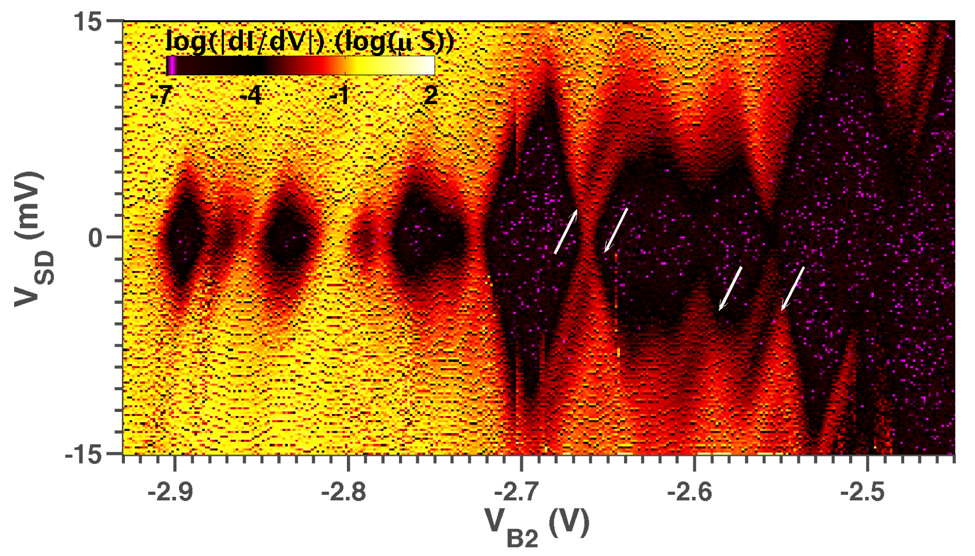
Energy spectroscopy was used to further characterize the device. The numerical differential conductance with varying and is suppressed periodically by Coulomb blockade, as shown in figure 4. The Coulomb diamonds are reasonably well defined and exhibit a single period, as evidenced by the parallel peaks in Fig. 3. The shape of the diamonds is most likely modulated by fluctuations in the conductance elsewhere in the device and the electrostatic environment, e.g. charge traps. At the diamond edges the electrochemical potential of the corresponding Coulomb island is resonant with either source or drain potential and single holes tunnel through the device. Most Coulomb diamonds close at zero source-drain bias, again indicating transport through a single island. changes the charge occupation of the island from to by moving from one Coulomb diamond to the next . The Coulomb diamonds have very similar shapes across a wide voltage range and reproduce in repeated measurements, indicating the robustness of the device.
The charging energy of the island varies from 5 to 10 meV. This corresponds to an island capacitance of 32 to 16 aF, which corresponds to a diameter of the island of about 76 to 38 nm in a classical disc capacitor model – where , with the diameter of the island. In the last few diamonds, lines of increased conductance appear parallel to the diamond edges at positive and negative bias. We attribute this to resonant tunneling features as a results of extra available states for tunneling lined up with either source or drain. These features may correspond to orbital excited states, although the origin cannot be determined based on these data alone Escott et al. (2010). The results in Fig. 4 show single-hole tunneling probed by energy spectroscopy, in which the present resonant tunneling features underline the ability to observe quantum states in these single-hole transistors.
To conclude, we have reported the fabrication and electronic characterization of p-type narrow-channel field-effect transistors in intrinsic silicon. Aluminum gate structures made on Si/SiO2 with electron-beam lithography were used to create and control a two-dimensional hole gas at the interface of silicon and silicon oxide. Hole transport at 4 K can be controlled by barrier and lead gates, such that Coulomb peaks appear at small source-drain bias. Highly regular Coulomb peak lines and closing Coulomb diamonds in energy spectroscopy clearly indicate single-hole tunneling in the many-hole regime. The strong capacitive coupling to each respective barrier gate suggest that single Coulomb islands are created underneath or in the vicinity of the controlling gate. These islands are caused by local potential fluctuations due to e.g. impurities or charge traps in the SiO2 or at the interface of Si and SiO2. Silicon is known for being extremely sensitive to disorder, owing to the large effective mass of the charge carriers, which is even higher for holes than for electrons. The evidence for resonant tunneling features in energy spectroscopy indicates that these devices have demonstrable quantum confinement, even at relatively high temperatures. Further optimization of the fabrication process will focus on (i) improvement the material quality of metal, oxide and semiconductor, e.g. lowering the charge trap density in the SiO2 and reducing the grain size in the Al, and (ii) minimization of disorder and roughness at the material interfaces, e.g. removing dangling bonds by introducing extra annealing steps. The resulting low-disorder hole quantum dots with tunable tunnel barriers pave the way towards control of single holes and single spins in silicon.
References
- Ladd et al. (2010) T. D. Ladd, F. Jelezko, R. Laflamme, Y. Nakamura, C. Monroe, and J. L. OBrien, Nature 464, 45 (2010).
- Loss and DiVincenzo (1998) D. Loss and D. P. DiVincenzo, Physical Review A 57, 120 (1998).
- van der Wiel et al. (2002) W. G. van der Wiel, S. De Franceschi, J. M. Elzerman, T. Fujisawa, S. Tarucha, and L. P. Kouwenhoven, Rev. Mod. Phys. 75, 1 (2002).
- Hanson et al. (2007) R. Hanson, L. P. Kouwenhoven, J. R. Petta, S. Tarucha, and L. M. K. Vandersypen, Reviews of Modern Physics 79, 1217 (2007).
- Jarillo-Herrero et al. (2004) P. Jarillo-Herrero, S. Sapmaz, C. Dekker, L. P. Kouwenhoven, and H. S. J. van der Zant, Nature 429, 389 (2004).
- Kuemmeth et al. (2008) F. Kuemmeth, S. Ilani, D. C. Ralph, and P. L. McEuen, Nature 452, 448 (2008).
- Simmons et al. (2007) C. B. Simmons, M. Thalakulam, N. Shaji, L. J. Klein, H. Qin, R. H. Blick, D. E. Savage, M. G. Lagally, S. N. Coppersmith, and M. A. Eriksson, Applied Physics Letters 91, 213103 (2007).
- Borselli et al. (2011) M. G. Borselli, K. Eng, E. T. Croke, B. M. Maune, B. Huang, R. S. Ross, A. A. Kiselev, P. W. Deelman, I. Alvarado-Rodriguez, A. E. Schmitz, M. Sokolich, K. S. Holabird, T. M. Hazard, M. F. Gyure, and A. T. Hunter, Applied Physics Letters 99, 063109 (2011).
- Zwanenburg et al. (2009) F. A. Zwanenburg, C. E. W. M. van Rijmenam, Y. Fang, C. M. Lieber, and L. P. Kouwenhoven, Nano Lett 9, 1071 (2009).
- Lim et al. (2009) W. H. Lim, F. A. Zwanenburg, H. Huebl, M. Möttönen, K. W. Chan, A. Morello, and A. S. Dzurak, Applied Physics Letters 95, 242102 (2009).
- Lansbergen et al. (2008) G. P. Lansbergen, R. Rahman, C. J. Wellard, I. Woo, J. Caro, N. Collaert, S. Biesemans, G. Klimeck, L. C. L. Hollenberg, and S. Rogge, Nature Physics 4, 656 (2008).
- Fuechsle et al. (2012) M. Fuechsle, J. Miwa, S. Mahapatra, H. Ryu, S. Lee, O. Warschkow, L. C. L. Hollenberg, G. Klimeck, and M. Y. Simmons, Nature Nanotechnology 7, 242 (2012).
- Prati et al. (2012) E. Prati, M. De Michielis, M. Belli, S. Cocco, M. Fanciulli, D. Kotekar-Patil, M. Ruoff, D. P. Kern, D. A. Wharam, J. Verduijn, et al., Nanotechnology 23, 215204 (2012).
- Steger et al. (2012) M. Steger, K. Saeedi, M. L. W. Thewalt, J. J. L. Morton, H. Riemann, N. V. Abrosimov, P. Becker, and H. J. Pohl, Science 336, 1280 (2012).
- Morton et al. (2011) J. J. L. Morton, D. R. McCamey, M. A. Eriksson, and S. A. Lyon, Nature 479, 345 (2011).
- Zwanenburg et al. (2012) F. A. Zwanenburg, A. S. Dzurak, A. Morello, M. Y. Simmons, L. C. L. Hollenberg, G. Klimeck, S. Rogge, S. N. Coppersmith, and M. A. Eriksson, arXiv preprint arXiv:1206.5202 (2012).
- Pla et al. (2012) J. Pla, K. Tan, J. Dehollain, W. Lim, J. Morton, D. Jamieson, A. Dzurak, and A. Morello, Nature 489, 541 (2012).
- Pla et al. (2013) J. J. Pla, K. Y. Tan, J. P. Dehollain, W. H. Lim, J. J. L. Morton, F. A. Zwanenburg, D. N. Jamieson, A. S. Dzurak, and A. Morello, arXiv preprint arXiv:1302.0047 (2013).
- Nowack et al. (2007) K. C. Nowack, F. H. L. Koppens, Y. V. Nazarov, and L. M. K. Vandersypen, Science 318, 1430 (2007).
- Laird et al. (2007) E. A. Laird, C. Barthel, E. I. Rashba, C. M. Marcus, M. P. Hanson, and A. C. Gossard, Physical review letters 99, 246601 (2007).
- Pioro-Ladriere et al. (2008) M. Pioro-Ladriere, T. Obata, Y. Tokura, Y.-S. Shin, T. Kubo, K. Yoshida, T. Taniyama, and S. Tarucha, Nature Physics 4, 776 (2008).
- Nadj-Perge et al. (2010) S. Nadj-Perge, S. M. Frolov, E. P. A. M. Bakkers, and L. P. Kouwenhoven, Nature 468, 1084 (2010).
- Pribiag et al. (2013) V. Pribiag, S. Nadj-Perge, S. Frolov, J. Berg, I. van Weperen, S. Plissard, E. Bakkers, and L. Kouwenhoven, Nature Nanotechnology (2013).
- Angus et al. (2007) S. J. Angus, A. J. Ferguson, A. S. Dzurak, and R. G. Clark, Nano Letters 7, 2051 (2007).
- Li et al. (2013) R. Li, F. E. Hudson, A. S. Dzurak, and A. R. Hamilton, (2013), arXiv:1304.2871 [cond-mat.mes-hall] .
- Escott et al. (2010) C. C. Escott, F. A. Zwanenburg, and A. Morello, Nanotechnology 21, 274018 (2010).