Charge Relaxation in a Single Electron Si/SiGe Double Quantum Dot
Abstract
We measure the interdot charge relaxation time of a single electron trapped in an accumulation mode Si/SiGe double quantum dot. The energy level structure of the charge qubit is determined using photon assisted tunneling, which reveals the presence of a low lying excited state. We systematically measure as a function of detuning and interdot tunnel coupling and show that it is tunable over four orders of magnitude, with a maximum of 45 s for our device configuration.
pacs:
85.35.Gv, 73.21.La, 73.63.KvSemiconductor quantum dots have been widely used as probes of fundamental quantum physics and to implement charge and spin qubits Loss and DiVincenzo (1998); Hanson et al. (2007). Coherent manipulation and two-qubit entanglement have been demonstrated in GaAs double quantum dots (DQDs) and error correction techniques such as dynamic decoupling have been employed to suppress decoherence Petta et al. (2005); Taylor et al. (2007); Bluhm et al. (2011); Shulman et al. (2012). As an alternative host material, Si holds promise for ultra-coherent spin qubits due to weak spin-orbit coupling, a centrosymmetric lattice (no piezo-phonon coupling), and an established route to isotopic purification Morello et al. (2010); Xiao et al. (2010); Simmons et al. (2011); Prance et al. (2012); Maune et al. (2012). Spin lifetimes of 6 seconds have been measured in Si and isotopically purified 28Si crystals can support spin coherence times as long as 4 seconds Morello et al. (2010); Tyryshkin et al. (2012).
While Si closely approximates a “semiconductor vacuum” for electron spins, its electronic band structure leads to potential complications that are absent in the conventional GaAs/AlGaAs two-dimensional electron gas (2DEG) system Awschalom et al. (2013). First, the 3 times larger effective mass of electrons in Si requires depletion gate patterns to be scaled down significantly in order to achieve orbital level spacings comparable to those obtained in GaAs. Second, the band structure of bulk Si consists of six degenerate valleys, which introduces an additional decoherence pathway Ando et al. (1982). Valley degeneracy is partially lifted by uniaxial strain in a Si/SiGe heterostructure Schäffler (1997). However, the energy splitting between the lowest two valleys is highly sensitive to device specifics, such as step-edges in the quantum well Goswami et al. (2007); Friesen and Coppersmith (2010); Maune et al. (2012). Detailed measurements of the low lying energy level structure, and the timescales that govern energy relaxation between these levels, are therefore needed in Si quantum dots tah .
In this Letter, we systematically measure the interdot relaxation time of a single electron trapped in a Si DQD as a function of detuning and interdot tunnel coupling . We demonstrate a four order of magnitude variation in using a single depletion gate and obtain = 45 s for weak interdot tunnel couplings Petta et al. (2004). We also use photon assisted tunneling (PAT) to probe the energy level structure of the single electron system, demonstrating spectroscopy with an energy resolution of 1 eV. In contrast with single electron GaAs dots, we observe low lying excited states 55 eV above the ground state, an energy scale that is consistent with previously measured valley splittings Goswami et al. (2007); Maune et al. (2012).
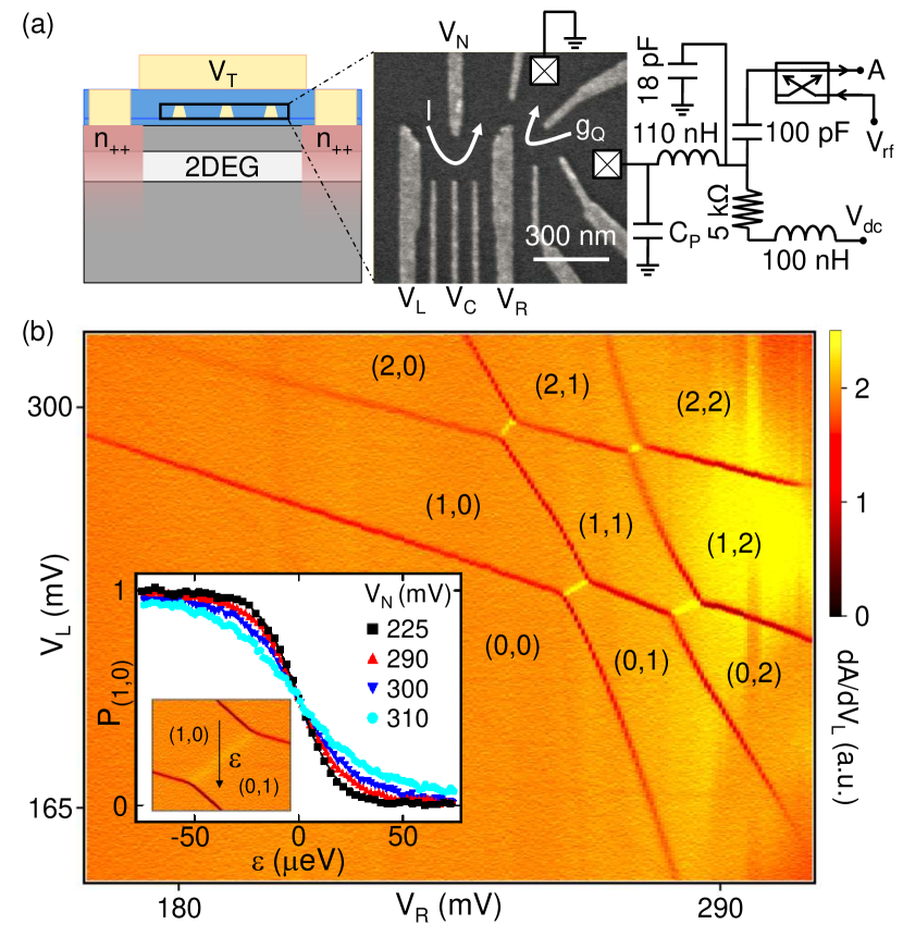
Measurements are performed on an accumulation mode Si/SiGe DQD. We apply a top gate voltage = 2 V to accumulate carriers in a Si quantum well located 40 nm below the surface of the wafer [see Fig. 1(a)]. The resulting 2DEG has an electron density of and a mobility of 70,000 . A 100 nm thick layer of Al2O3 separates the top gate from the depletion gates, which are arranged to define a DQD and a single dot charge sensor.
We first demonstrate single electron occupancy using radio frequency (rf) reflectometry Schoelkopf et al. (1998). A single quantum dot is coupled to a resonant circuit with resonance frequency = 431.8 MHz [Fig. 1(a)] and used as a high sensitivity charge detector Barthel et al. (2010). The reflected amplitude is a sensitive function of the conductance of the single dot sensor, , which is modulated by charge transitions in the DQD. We map out the DQD charge stability diagram in Fig. 1(b) by plotting the numerical derivative as a function of and . No charging transitions are observed in the lower left corner of the charge stability diagram, indicating that the DQD has been completely emptied of free electrons. We identify this charge configuration as (0,0), where (,) indicates the number of electrons in the left and right dots.
The device is operated as a single electron charge qubit near the (1,0)–(0,1) interdot charge transition. Charge dynamics are governed by the Hamiltonian = , where are the Pauli matrices. We demonstrate tunable interdot tunnel coupling in the single electron regime by measuring the left dot occupation as a function of detuning [Fig. 1(b), inset] Loss and DiVincenzo (1998); nakamura1999 ; Petta et al. (2005). Qubit occupation is described by
| (1) |
where is Boltzmann’s constant, 100 mK is the electron temperature, and is the qubit energy splitting DiCarlo et al. (2004); Petta et al. (2004); Simmons et al. (2009). With = 225 mV, the interdot charge transition is thermally broadened as 2 . Increasing by adjusting leads to further broadening of the interdot transition. For = 290, 300 and 310 mV we extract = 3.8, 5.9 and 9.0 GHz by fitting the data to Eq. 1. These results show that the interdot tunnel coupling can be sensitively tuned in the single electron regime in Si.
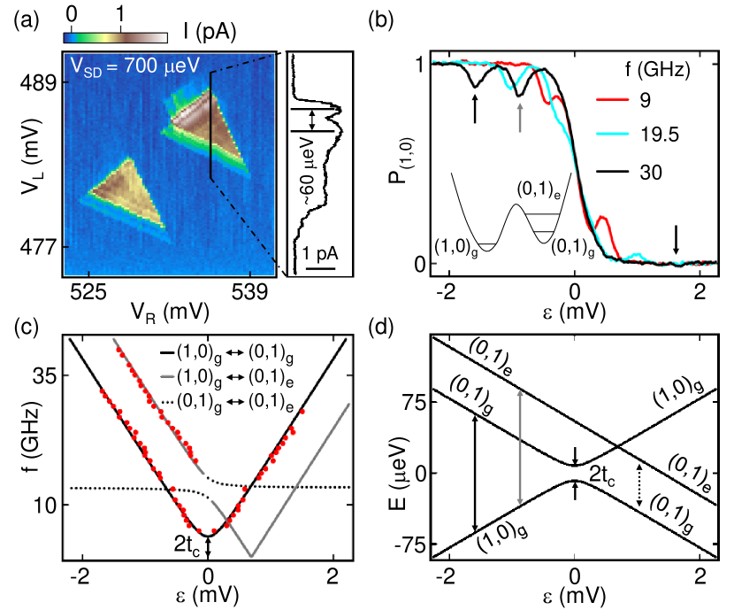
We investigate the DQD energy level structure in Fig. 2(a), where we plot the current as a function of and with a fixed source-drain bias = 700 eV van der Wiel et al. (2002). In contrast with GaAs devices, the current in the finite bias triangles is not a smooth function of gate voltage. In particular, we observe a small resonance 60 eV away from the interdot charge transition, suggesting the existence of a low-lying excited state in one of the dots. In a few electron GaAs DQD, orbital excited states are typically several meV higher in energy than the ground state Johnson et al. (2005).
Higher energy resolution is obtained using PAT spectroscopy, in which microwaves drive charge transitions when the photon energy matches the qubit splitting, = , where is the photon frequency and is Planck’s constant. PAT transitions are directly observed as deviations from the ground state occupation in measurements of as a function of detuning [compare Fig. 2(b) and the inset to Fig. 1(b)]. For 15 GHz, the PAT peaks are symmetric around = 0 and shift to larger detuning with increasing photon energy, consistent with a simple two level interpretation C. H. van der Wal (2000); Petta et al. (2004). However, for 15 GHz, an additional PAT peak emerges at negative detuning and is not accompanied by a corresponding PAT peak at positive detuning. Figure 2(c) shows the extracted transition frequencies as a function of detuning.
The data are fit using a three level Hamiltonian that includes the left dot ground state , the right dot ground state , and a right dot excited state , as sketched in the inset of Fig. 2(b) Sup . We obtain best fit values of = 1.9 GHz and = 55 eV, consistent with the data shown in the inset of Fig. 1(b) and Fig. 2(a). Within the 1 eV resolution of our measurement, we do not observe anti-crossings associated with . The energy eigenstates obtained from the model are plotted as a function of detuning in Fig. 2(d). For comparison, an excited state is observed in the left quantum dot in a second device (Device 2), with = 64 eV Sup . For both devices, the excited state energy is highly sensitive to and , suggesting that it is not purely orbital in origin Friesen and Coppersmith (2010).
Several additional features observed in the data are explained by the three level model. The intradot charge transition [dotted line, Fig. 2(c)] is not visible since the charge detector is only sensitive to interdot charge transitions. We also note that the PAT peak is not visible at positive detuning. At low temperatures, the qubit population resides in the ground state , preventing microwave transitions from to . Finally, the PAT peak is suppressed when due to population trapping in .
We measure the interdot charge relaxation time by applying microwaves to with a 50 duty cycle and varying the pulse period [Fig. 3(a)]. We focus on the transition at negative detuning, where the high energy state is not populated. Simulations of as a function of time, , for = 1 s are shown in Fig. 3(a) for three realistic values of . During the first half of the pulse cycle, microwaves drive the charge transition, resulting in an average = 0.5. The microwave excitation is then turned off, leading to charge relaxation during the second half of the pulse cycle, with approaching 1 on a timescale set by .
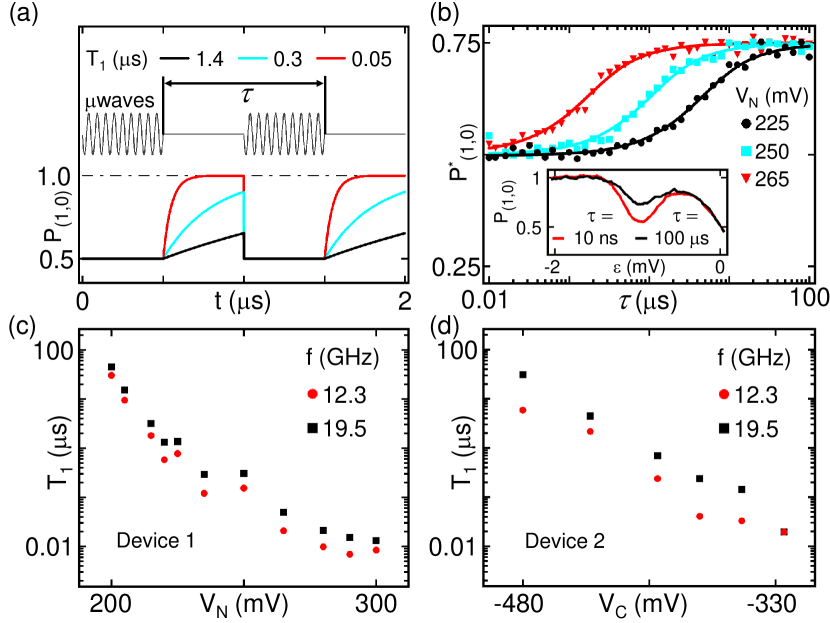
In the inset of Fig. 3(b), we plot as a function of detuning for = 10 ns and = 100 s. As expected, the PAT peak is smaller for longer periods due to charge relaxation. Specifically, in the limit , there is not sufficient time for relaxation to occur during the second half of the pulse cycle, leading to a time averaged value of = 0.5. In contrast, in the limit , relaxation happens quickly, leaving = 1 for the majority of the second half of the pulse cycle. Due to experimental limitations, such as frequency dependent attenuation in the coax lines and finite pulse rise times at small , we are unable to drive the transitions to saturation for some device configurations. To extract we therefore fit the raw data as a function of to the form
| (2) |
where and account for the limited visibility of the PAT peaks Petta et al. (2004); Sup . Extracted values are insensitive to the rescaling of the data via and .
The interdot charge relaxation rate is strongly dependent on the interdot tunnel coupling. This variation is directly visible in the data shown in Fig. 3(b) for = 225, 250 and 265 mV. To facilitate a direct comparison of the data, we plot the normalized electron occupation = 0.5 + 0.25 , using the values of and extracted from fits to Eq. 2 Sup . In Fig. 3(c), we plot over a wide range of for two different excitation frequencies. We see a longer characteristic relaxation time for larger interdot barrier heights, with a maximum observed value of 45 s. The same overall trend is observed in data from Device 2 [Fig. 3(d)] where the interdot tunnel coupling was tuned using . Interdot tunnel coupling is only measurable in charge sensing when 2 DiCarlo et al. (2004). For Device 1 [see Fig. 3(c)] we obtain 2 = 2.4, 3.8 and 5.9 GHz for = 280, 290 and 300 mV and for Device 2 [see Fig. 3(d)] we obtain 2 = 3.2 GHz for = -325 mV.
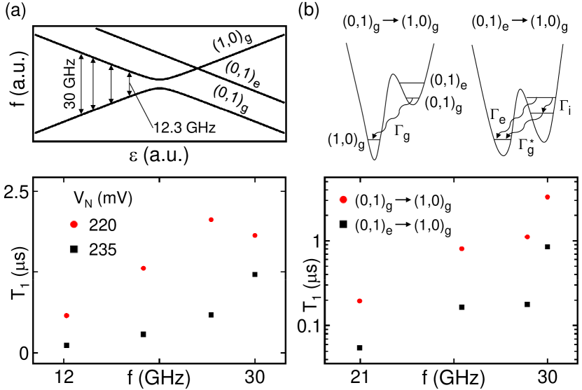
The detuning dependence of is investigated in Fig. 4(a), where we plot as a function of for the transition nakamura1999 ; Petta et al. (2005). Data are taken at = 12.3, 19.5, 25.9 and 30.0 GHz, as indicated by the arrows in the energy level diagram in the upper panel of Fig. 4(a). Our data indicate that increases weakly as a function of detuning for the range of frequencies accessible in our cryostat.
To further investigate the excited state, we measure for the and the relaxation processes at the same values of [bottom panel of Fig. 4(b)]. In contrast with the relaxation process, can relax via two distinct pathways [top panel of Fig. 4(b)]. The first relaxation process is a direct transition from with a rate , while the second pathway proceeds via intradot charge relaxation to with a rate followed by an interdot transition to with rate . We find that relaxation is faster than relaxation for the same energy splitting. The shorter excited state lifetime is consistent with either a fast direct relaxation rate or fast intradot relaxation followed by an interdot transition. Assuming = (since the level detuning is the same) and taking the measured excited state = 55 ns at = 21.0 GHz, we can make a rough lower bound estimate Fujisawa et al. (2002).
We modify the results of Raith et al. to allow the calculation of phonon mediated charge relaxation rates considering only intravalley relaxation in the far detuned limit (), assuming Gaussian wavefunctions for the non-hybridized charge states, with dot radius and dot separation 2 Raith et al. (2012); Sup . The electron-phonon coupling Hamiltonian in a Si quantum well takes the form
| (3) |
where
| (4) |
Here () are the annihilation (creation) operators for phonons belonging to branch ( = TA1, TA2 for transverse phonons and = LA for longitudinal phonons) with wave vector , and speed of sound in Si . is the volume of the Si quantum well layer and is the density of Si. and are the shear and dilation deformation potential constants and and are the phonon unit polarization vector and the phonon unit wave vector Raith et al. (2012). Using realistic parameters, values calculated in this model are in order of magnitude agreement with our data Sup . However, the predictions are exponentially sensitive to and , quantities that are difficult to accurately determine. Moreover, the model predicts a relaxation rate that increases with energy splitting for the range of detunings accessed in our experiment, following the power law , whereas we observe a rate that decreases weakly with increasing detuning Sup . This discrepancy may be due to a detuning dependent or contributions from other relaxation channels, such as charge noise Astafiev et al. (2004).
In summary, we have measured charge relaxation times in a single electron Si/SiGe DQD, demonstrating a four order of magnitude variation of with gate voltage. Energy level spectroscopy indicates the presence of a low-lying excited state. From the estimated dot radius 38 nm, we expect orbital level spacings on the order of 1 meV, a factor of 18 larger than the value obtained from PAT spectroscopy ( = 55 eV) Kouwenhoven et al. (1997). This suggests that the low-lying excited state is a valley-orbit mixed state Dzu .
Acknowledgements.
We acknowledge helpful discussions with Jaroslav Fabian, Xuedong Hu, Debayan Mitra, Martin Raith, Peter Stano, James Sturm, and Charles Tahan. We thank Norm Jarosik for technical contributions. Research sponsored by the United States Department of Defense with partial support from the NSF through the Princeton Center for Complex Materials (DMR-0819860) and CAREER program (DMR-0846341). C. P. acknowledges partial support from FQRNT. The views and conclusions contained in this document are those of the authors and should not be interpreted as representing the official policies, either expressly or implied, of the United States Department of Defense or the U.S. Government. Approved for public release, distribution unlimited.References
- Loss and DiVincenzo (1998) \BibitemOpen\bibfieldauthor D. Loss and D. P. DiVincenzo, \bibfieldjournal Phys. Rev. A 57, 120 (1998)\BibitemShutNoStop
- Hanson et al. (2007) \BibitemOpen\bibfieldauthor R. Hanson, L. P. Kouwenhoven, J. R. Petta, S. Tarucha, and L. M. K. Vandersypen, \bibfieldjournal Rev. Mod. Phys. 79, 1217 (2007)\BibitemShutNoStop
- Petta et al. (2005) \BibitemOpen\bibfieldauthor J. R. Petta, A. C. Johnson, J. M. Taylor, E. A. Laird, A. Yacoby, M. D. Lukin, C. M. Marcus, M. P. Hanson, and A. C. Gossard, \bibfieldjournal Science 309, 2180 (2005)\BibitemShutNoStop
- Taylor et al. (2007) \BibitemOpen\bibfieldauthor J. M. Taylor, J. R. Petta, A. C. Johnson, A. Yacoby, C. M. Marcus, and M. D. Lukin, \bibfieldjournal Phys. Rev. B 76, 035315 (2007)\BibitemShutNoStop
- Bluhm et al. (2011) \BibitemOpen\bibfieldauthor H. Bluhm, S. Foletti, I. Neder, M. Rudner, D. Mahalu, V. Umansky, and A. Yacoby, \bibfieldjournal Nat. Phys. 7, 109 (2011)\BibitemShutNoStop
- Shulman et al. (2012) \BibitemOpen\bibfieldauthor M. D. Shulman, O. E. Dial, S. P. Harvey, H. Bluhm, V. Umansky, and A. Yacoby, \bibfieldjournal Science 336, 202 (2012)\BibitemShutNoStop
- Morello et al. (2010) \BibitemOpen\bibfieldauthor A. Morello et al., \bibfieldjournal Nature (London) 467, 687 (2010)\BibitemShutNoStop
- Xiao et al. (2010) \BibitemOpen\bibfieldauthor M. Xiao, M. G. House, and H. W. Jiang, \bibfieldjournal Phys. Rev. Lett. 104, 096801 (2010)\BibitemShutNoStop
- Simmons et al. (2011) \BibitemOpen\bibfieldauthor C. B. Simmons et al., \bibfieldjournal Phys. Rev. Lett. 106, 156804 (2011)\BibitemShutNoStop
- Prance et al. (2012) \BibitemOpen\bibfieldauthor J. R. Prance et al., \bibfieldjournal Phys. Rev. Lett. 108, 046808 (2012)\BibitemShutNoStop
- Maune et al. (2012) \BibitemOpen\bibfieldauthor B. M. Maune et al., \bibfieldjournal Nature (London) 481, 344 (2012)\BibitemShutNoStop
- Tyryshkin et al. (2012) \BibitemOpen\bibfieldauthor A. M. Tyryshkin et al., \bibfieldjournal Nat. Mater. 11, 143 (2012)\BibitemShutNoStop
- Awschalom et al. (2013) \BibitemOpen\bibfieldauthor D. D. Awschalom, L. C. Bassett, A. S. Dzurak, E. L. Hu, and J. R. Petta, \bibfieldjournal Science 339, 1174 (2013)\BibitemShutNoStop
- Ando et al. (1982) \BibitemOpen\bibfieldauthor T. Ando, A. B. Fowler, and F. Stern, \bibfieldjournal Rev. Mod. Phys. 54, 437 (1982)\BibitemShutNoStop
- Schäffler (1997) \BibitemOpen\bibfieldauthor F. Schäffler, \bibfieldjournal Semicond. Sci. Technol. 12, 1515 (1997)\BibitemShutNoStop
- Goswami et al. (2007) \BibitemOpen\bibfieldauthor S. Goswami et al., \bibfieldjournal Nat. Phys. 3, 41 (2007)\BibitemShutNoStop
- Friesen and Coppersmith (2010) \BibitemOpen\bibfieldauthor M. Friesen and S. N. Coppersmith, \bibfieldjournal Phys. Rev. B 81, 115324 (2010)\BibitemShutNoStop
- (18) \BibitemOpenC. Tahan and R. Joynt, arXiv:1301.0260\BibitemShutNoStop
- Petta et al. (2004) \BibitemOpen\bibfieldauthor J. R. Petta, A. C. Johnson, C. M. Marcus, M. P. Hanson, and A. C. Gossard, \bibfieldjournal Phys. Rev. Lett. 93, 186802 (2004)\BibitemShutNoStop
- Schoelkopf et al. (1998) \BibitemOpen\bibfieldauthor R. J. Schoelkopf, P. Wahlgren, A. A. Kozhevnikov, P. Delsing, and D. E. Prober, \bibfieldjournal Science 280, 1238 (1998)\BibitemShutNoStop
- Barthel et al. (2010) \BibitemOpen\bibfieldauthor C. Barthel, M. Kjærgaard, J. Medford, M. Stopa, C. M. Marcus, M. P. Hanson, and A. C. Gossard, \bibfieldjournal Phys. Rev. B 81, 161308 (2010)\BibitemShutNoStop
- (22) Y. Nakamura, Yu. A. Pashkin, J. S. Tsai, Nature 398, 786 (1999).
- DiCarlo et al. (2004) \BibitemOpen\bibfieldauthor L. DiCarlo, H. J. Lynch, A. C. Johnson, L. I. Childress, K. Crockett, C. M. Marcus, M. P. Hanson, and A. C. Gossard, \bibfieldjournal Phys. Rev. Lett. 92, 226801 (2004)\BibitemShutNoStop
- Simmons et al. (2009) \BibitemOpen\bibfieldauthor C. B. Simmons, M. Thalakulam, B. M. Rosemeyer, B. J. Van Bael, E. K. Sackmann, D. E. Savage, M. G. Lagally, R. Joynt, M. Friesen, S. N. Coppersmith, and M. A. Eriksson, \bibfieldjournal Nano Letters 9, 3234 (2009)\BibitemShutNoStop
- van der Wiel et al. (2002) \BibitemOpen\bibfieldauthor W. G. van der Wiel, S. De Franceschi, J. M. Elzerman, T. Fujisawa, S. Tarucha, and L. P. Kouwenhoven, \bibfieldjournal Rev. Mod. Phys. 75, 1 (2002)\BibitemShutNoStop
- Johnson et al. (2005) \BibitemOpen\bibfieldauthor A. C. Johnson, C. M. Marcus, M. P. Hanson, and A. C. Gossard, \bibfieldjournal Phys. Rev. B 71, 115333 (2005)\BibitemShutNoStop
- C. H. van der Wal (2000) \BibitemOpen\bibfieldauthor C. H. van der Wal, A. C. J. ter Haar, F. K. Wilhelm, R. N. Schouten, C. J. P. M. Harmans, T. P. Orlando, S. Lloyd, and J. E. Mooij, \bibfieldjournal Science 290, 773 (2000)\BibitemShutNoStop
- (28) \BibitemOpenSee Supplemetary Material at [url] for more details\BibitemShutNoStop
- Fujisawa et al. (2002) \BibitemOpen\bibfieldauthor T. Fujisawa, D. G. Austing, Y. Tokura, Y. Hirayama, and S. Tarucha, \bibfieldjournal Nature (London) 419, 278 (2002)\BibitemShutNoStop
- Raith et al. (2012) \BibitemOpen\bibfieldauthor M. Raith, P. Stano, and J. Fabian, \bibfieldjournal Phys. Rev. B 86, 205321 (2012)\BibitemShutNoStop
- Astafiev et al. (2004) \BibitemOpen\bibfieldauthor O. Astafiev, Y. A. Pashkin, Y. Nakamura, T. Yamamoto, and J. S. Tsai, \bibfieldjournal Phys. Rev. Lett. 93, 267007 (2004)\BibitemShutNoStop
- Kouwenhoven et al. (1997) \BibitemOpen\bibfieldauthor L. P. Kouwenhoven, C. M. Marcus, P. L. McEuen, S. Tarucha, R. M. Westervelt, and N. S. Wingreen, in Mesoscopic Electron Transport, series E, Vol. 345, edited by L. L. Sohn, L. P. Kouwenhoven, and G. Schon, NATO Advanced Studies Institute (Kluwer Academic, Dordrecht, 1997)\BibitemShutNoStop
- (33) \BibitemOpenC. H. Yang, A. Rossi, R. Ruskov, N. S. Lai, F. A. Mohiyaddin, S. Lee, C. Tahan, G. Klimeck, A. Morello, and A. S. Dzurak, arXiv:1302.0983\BibitemShutNoStop