Simulation of nanostructure-based high-efficiency solar cells: challenges, existing approaches and future directions
Abstract
Many advanced concepts for high-efficiency photovoltaic devices exploit the peculiar optoelectronic properties of semiconductor nanostructures such as quantum wells, wires and dots. While the optics of such devices is only modestly affected due to the small size of the structures, the optical transitions and electronic transport can strongly deviate from the simple bulk picture known from conventional solar cell devices. This review article discusses the challenges for an adequate theoretical description of the photovoltaic device operation arising from the introduction of nanostructure absorber and/or conductor components and gives an overview of existing device simulation approaches.
Index Terms:
solar energy, photovoltaic effect, nanostructures, simulationI Introduction
The past decade has witnessed a strong increase in the demand of clean electricity production based on renewable energy sources and an associated exponential growth of installed photovoltaic (PV) power capacity. The largest share of the actual PV electricity supply is still based on crystalline silicon wafer solar cells (SC). However, this technology, though mature and highly developed, suffers from several fundamental limitations. First of all, the energy conversion efficiency of this type of single junction SC device is limited by the fundamental laws of thermodynamics [1] to below 40% even at full concentration. Due to the low absorption originating in the indirect nature of optical transitions in crystalline silicon, a large amount of semiconductor material of high quality is required to approach the limiting efficiency. Furthermore, with the successful reduction of manufacturing costs via optimization of the individual production steps at industrial scale, efficiency becomes a central issue. This demand for higher PV energy conversion efficiencies has in the past decade led to the emergence of a whole new generation of SC concepts [2, 3], which all aim at exceeding the single junction efficiency limit through the reduction of fundamental losses. Well-known representatives are the concepts based on enhanced spectrum utilization and reduced thermalization losses via the use of multiple junctions[4], intermediate bands [5], multiple exciton generation [6] or hot carrier effects [7].
While these concepts differ widely in the physical mechanisms exploited, what they have in common is that they are largely based on artificially engineered materials with designed optoelectronic properties, like semiconductor nanostructures (NS) such as quantum wells, wires and dots, offering size-, geometry- and composition-tunable characteristics [8]. This deviation from bulk behaviour needs to be taken into account at the time of describing the device operation mechanisms, a requirement which may preclude the use of standard macroscopic device simulation models commonly used in bulk photovoltaics. Similar issues are encountered in the field of NS-based light emitting and amplifying devices, however, the regime of operation is inverted in SCs, since the light needs to be trapped and the charge carriers are to be extracted. While light-trapping techniques have been successfully implemented, leading to a substantial efficiency enhancement, the increase of collection efficiency remains a critical issue, mainly due to the strong interaction of charge carriers with their environment and the large number of interfaces associated with the NS. In this review, we will thus focus on SC devices where the NS possess an electronic functionality as an electrically coupled absorber material, and where both carrier generation as well as extraction are being considered. Due to the emphasis on high efficiencies rather than low cost, only concepts based on regular inorganic NS shall be considered. These two restrictions exclude the vast and rapidly growing fields of computational tools for nanophotonic light management [9, 10] on the one hand, and for organic and hybrid SC [11, 12] (which are both also largely based on NS but cannot be counted among the high-efficiency concepts) on the other hand. Also, compared to more established technologies, the concepts presented here have not in all cases been successfully implemented yet, and experimental device characteristics are thus of limited validity for a reliable verification of the models providing the theoretical predictions for the device performance.
The review is organized as follows. In section II, the use of NS in the implementation of different specific high efficiency concepts is discussed. In a third section, the requirements for appropriate models specific to the related device structures are formulated. Based on these findings, different classes of models are identified in section IV and positioned with respect to a general hierarchy of device simulation approaches. Section V provides an overview of existing implementations for the most important types of NS-based SC, namely those based on quantum wells (QW) and quantum dots (QD) with both optical and electronic functionality. Section VI summarizes the main remaining challenges and open problems in nanostructured PV device simulation and thus points at potential directions of future developments. Section VII concludes the review.
II Nanostructure-based implementation of high efficiency solar cells
The idea of utilizing low dimensional structures for novel high efficiency SC concepts dates back to the early days of epitaxial semiconductor growth in the eighties [13, 14], and became increasingly popular after the group of Barnham at Imperial College put forward the concept of the quantum well solar cell (QWSC) in the early nineties [15], which still represents the prototype of a successfully implemented NS PV device. At the beginning of the last decade, most of the concepts investigated today had been conceived [16]. In 2001, NS for photovoltaics was the topic of a landmark workshop at the MPI Dresden, which, together with the accompanying publications, boosted both popularity and impact of this field of research. Two important representatives of these concepts with extensive utilization of NS - the multi quantum well/dot single junction SC (MQWSC/MQDSC) and the QW/QD superlattice (QWSL/QDSL) multi-junction SC - shall briefly be reviewed below.
II-A MQWSC/MQDSC - band gap engineering for single junction devices
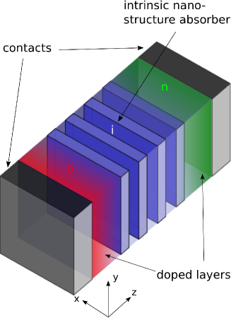
As one of the first NS-based high efficiency concepts being experimentally realized, the QWSC now represents the most mature and industry relevant technology in this field. The main idea of the concept is to extend the absorption range of a high band gap material via the insertion of thin layers of lower band gap material in the intrinsic absorber region of a single junction PV device, where the effective band gap is then determined by the quantum well states. In the MQW concept (Fig. 1), the quantum wells are separated by thick regions of high band gap material, and in order to contribute to the photocurrent, the charge carriers generated in the quantum wells need to escape to the conduction band of the bulk material via thermionic emission or phonon-assisted tunneling (Fig. 2). The original hope for an independent optimizability of open circuit voltage and short circuit current via the use of high and low band gap materials [15] was soon shown to fail on thermodynamical grounds [17, 18, 19]: the was found to correspond rather to that of a bulk cell with an effective band gap determined by the nanostructure states. On the other hand, could be effectively enhanced, as the escape process proved to be highly efficient with probabilities close to unity at room temperature for effective barrier potentials of the order of 0.1-0.2 eV. The use of strain-balancing techniques allowed to overcome initial difficulties with strain-related dislocation formation [20], such that dislocation free samples with up to 65 QW layers could be grown, and a maximum efficiency of 28.3% could be achieved (under high concentration)[21], which corresponds to the highest value for a NS-based single junction SC architecture. There are similar approaches based on quantum dot layers [22, 23], which have the additional advantage of allowed radiative subband transitions, however, the QDs need either be large enough or strongly coupled in order to provide a quasi-continuum of subgap states. In contrast to the QW devices, formation of dislocations and other surface defects, as well as achieving a high enough QD density for sufficient absorption are still a critical issues in QD-based solar cell devices, and the resulting loss is higher.
II-B QWSL/QDSL-multi-junction SCs
Multi-junction SC architectures rely on the vertical stacking of absorber materials with decreasing band gap energies, which allows for a better utilization of the solar spectrum as thermalization losses are reduced. Concentrator architectures with multi-junction cells based on III-V semiconductor alloys yield record efficiencies up to 44% [24]. The single component cells are connected in series via tunnel junctions, the voltages of the subcells are thus added, while the current needs to be matched over the whole absorber stack. This current matching condition puts severe limitations to the optimum combination of band gap values. Depending on the material system, it is difficult or even impossible to find a bulk absorber with the required properties. In this situation, superstructures of coupled quantum wells, wires or dots can be used to engineer absorber components with the desired band gap (Fig. 3). The coupling of the QW/QD gives rise to a delocalization of the confined states, which for periodically arranged nanostructures results in the formation of so-called minibands with tunable band edges. As opposed to the case of the MQW or MQD architectures, transport of charge carriers generated in miniband states is also mediated by the latter and not by the extended states of the host material. Due to the prominent position of crystalline silicon SC, a large amount of research was dedicated to the fabrication of all-silicon tandem SC with a superlattice of silicon nanocrystals in silicon-based dielectric matrix material as high-band gap absorber component [25, 26]. However, while the tunability of the absorption edge is routinely achieved, efficient charge carrier transport remains a true challenge, and there exists up to now no working superlattice cell relying entirely on transport in miniband states. To get a notion for the challenges associated with this concept, one first should remember that, as a general fact, the coupling of NS exhibiting quantum confinement leads to a reduction of the confinement in the dimension of the coupling. It is thus impossible to achieve at the same time high band gap values and high carrier mobilities by using a quantum well superlattice where confinement is only present in the transport direction. On the other hand, the delocalization of the wave functions in the case of quantum dot superlattices is very sensitive to irregularities in shape or position of the dots which are always present in real samples. The most advantageous architecture would thus be composed of conducting filaments or nanowires with sufficient radial confinement, avoiding the conflict between localization for band gap tuning and delocalization for charge carrier extraction by separating of the respective dimensions.
III Modelling requirements
On a very fundamental level of description, a SC converts light into electrical energy. Any theory suitable for the modelling of a SC device thus needs to be able to describe the fundamental photovoltaic processes of charge carrier generation by photon absorption and charge carrier extraction via carrier selective contacts, which usually involves transport. Even in ideal absorber materials, the principle of detailed balance demands the presence of radiative recombination by spontaneous and stimulated emission, and in the high-injection regime, the PV performance of an ideal absorber is limited by the Auger recombination process, which is also intrinsic, i.e., can not be avoided and needs thus be considered for any realistic estimate of limiting efficiency.
Depending on the functionality of the NS within the SC device, some or all of these processes are affected by the peculiar physical properties of the nanoscale component, with major implications for the requirements on any suitable simulation approach. Let us consider in the following the different stages of the photovoltaic energy conversion with focus on these modelling requirements.
III-A Exciton generation by photon absorption
The interaction of electromagnetic radiation with the electrons of a solid results in electronic excitations, whose nature depends on the energy and polarization of the incident radiation field and on the available electronic states. While this interaction is inherently nonlocal from the electronic point of view, generation is usually determined based on locally defined absorption coefficients that reflect all optical excitations possible at a given photon energy, weighted by their respective strength.
The main quantities determining the generation of excitons are, thus, the local value of the transverse electromagnetic field on the one hand, and the local value of the dipole or momentum matrix elements and of the density of occupied initial and empty final states of the optical transitions, respectively, on the other hand. While the transverse EM fields are barely affected by semiconductor NS in the range of few nm, the electronic quantities reflect the impact of symmetry breaking and wave function localization due to the departure from bulk material towards significant spatial variation of material properties on short length scales. There is, for instance, a contribution of direct transitions in silicon quantum dots, which is absent in bulk and is beneficial to the absorption [27, 28], and also an increase in oscillator strength due to larger overlap of electron and hole wave functions. Hence, the optical modelling is not essentially different from that for bulk or conventional thin film devices, but any suitable description of the light-matter coupling needs to reflect the nanoscale extensions of the absorber.
III-B Charge transport to carrier selective contacts
This is one of the most critical aspects in NS-based PV devices. Indeed, while the tayloring of the absorption via band structure engineering was shown to work out for a range of SC devices based on QW [29] or QD [30], the efficiency of carrier collection has until now remained below that in the bulk counterparts, in some cases on a dramatically poor level, especially in devices where transport proceeds via states with increased degree of localization. There are several reasons for the observed performance issue, which are associated with different stages in the extraction process, such as exciton dissociation, carrier escape and capture between localized and extended states, mobility issues associated with scattering and the virtual absence of true miniband formation in realistic situation, which shall be discussed below.
III-B1 Exciton dissociation
Since electrons and holes have to be extracted via separate contacts, the dissociation of the exciton and subsequent charge separation need to occur at some point in the device. In bipolar bulk SC, exciton binding energies are usually in the range of a few meV, resulting in thermal dissociation immediately after generation, and the generation can thus safely be described in terms of non-interacting electron-hole pairs. In isolated NS on the other hand, exciton binding energies can easily amount to multiples of [28], which can give rise to prominent excitonic features in the absorption and photocurrent spectra [31], and can severely inhibit an efficient charge separation and even result in a transport behaviour dominated by exciton diffusion, similar to the situation in organic SC devices, where a specially designed bulk-heterojunction interface is required for exciton dissociation. As a SC based on exciton diffusion is not likely to reach very high efficiencies, the description of excitons in the simulation of high-efficiency SC devices is primarily focused on the excitonic enhancement of optical transitions close to the effective band edge.
III-B2 Carrier escape and capture
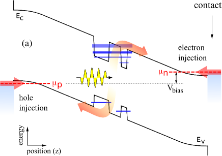
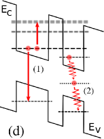
Basically, there are two types of NS-absorber-based SC devices. In the first case, the NS act as mere absorbers, with the charge carriers generated in localized states escaping to the extended states of the bulk host material via thermionic emission or phonon-assisted tunneling (Fig. 2c). A prototype example of this kind is the MQWSC with large spacing between the quantum wells. In this situation, the charge carrier extraction is limited by the efficiency of the escape process and by the probability of subsequent carrier capture in the lower-lying localized states of NS encountered on the way to the contacts. A realistic assessment of the device performance thus relies on an accurate determination of the associated rates.
III-B3 Carrier mobility and relaxation
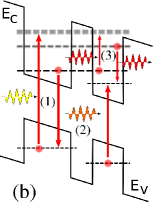
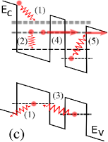
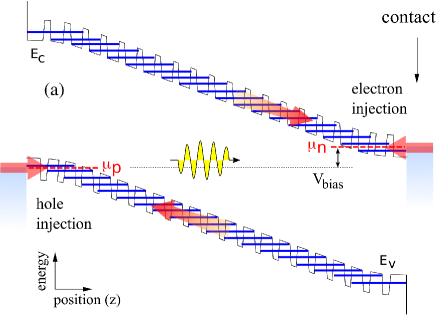
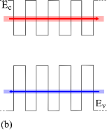
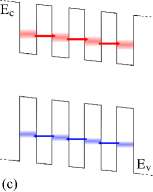
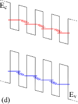
In the second type of NS-absorber-based solar cell device, the NS mediate not only the absorption, but also the carrier transport to the contacts (Fig. 4a). These states thus need to be to some degree extended, which amounts to the requirement of coupling between the single NS. Indeed, most of the concepts of this kind that have been proposed are based on the formation of minibands in superlattices of quantum wells or quantum dots (Fig. 4b). However, in realistic situations, due to the presence of internal fields and any kind of spatial and compositional disorder, the NS states usually show a high degree of localization, such that tunneling is restricted to nearest neighbors (Fig. 4c). In addition to inducing localization, these effects lead to a misalignement of energy levels in adjacent NS, with the formation of Wannier-Stark ladders in the extreme case of very strong fields [32], in which situation transport is only possible via an inelastic scattering process and is best described by hopping (Fig. 4d). Even in the ideal case of a perfect miniband, the associated Bloch mobility may be critically low, as in the case of silicon QD in dielectric matrix material [33]. In coupled QD systems, due to the sparsity of the DOS, the presence of charge on the NS can lead to pronounced shifts in the energy level structure [28], inhibiting transport ( Coulomb blockade regime). The bulk picture of charge carrier transport in band states does thus in general not provide a proper description of the real situation, which in addition to the remaining coherence and non-locality effects should include all the localization effects and scattering mechanisms required to overcome energetic misalignement. The modification of the electronic structure due to the presence of NS also affects the scattering processes responsible for the limitation of mobility and for carrier relaxation, such as electron-phonon interaction, which becomes especially relevant in devices where this form of energy dissipation should be suppressed, as in the hot carrier concept, and in the case where extraction distances are on the order of the mean free path and transport approaches the ballistic regime.
III-C Recombination
The poor transport properties exhibited by many of the NS-based SC devices would not be as detrimental as they are if recombination was limited to radiative processes, since radiative livetimes are still long enough to allow for carrier extraction, even though they are reduced in NS as compared to the bulk (due to localization and local reduction of the effective band gap). However, there is an inherent increase in surface area associated with the presence of NS, which are thus likely to act as centers of non-radiative recombination. In some cases, it is possible to reduce the NS-related defects via specially engineered strain-balancing techniques [34] or via passivation [35], but in general, the insertion of NS leads to losses in the open circuit voltage of the SC. Like for the generation process, a proper consideration of recombination processes requires a careful consideration of the wave functions and local density of NS states together with the occupation of these states in general non-equilibrium conditions.
IV Classification and hierarchy of models
Based on underlying assumptions, scope and predictive power, the majority of modelling approaches for
NS-based high-efficiency SC devices can be roughly categorized in three classes:
(i) Thermodynamic or detailed balance theories for ideal systems;
(ii) Models based on analytical or numerical solution of the macroscopic semiconductor transport equations.
The source and sink terms for carrier generation and recombination are included together with equations for the
rates of carrier exchange between localized and extended states (where separate microscopic models
for the localized states might be used);
(iii) Advanced quantum-kinetic models reflecting the microscopic mechanisms of the photovoltaic processes.
While the models in the first category rely on highly idealized assumptions and therefore primarily provide upper limiting efficiencies, the latter two classes of approaches describe more realistic situations, including an estimate of the relevant loss processes, and aim at reproducing real device characteristics.
IV-A Thermodynamic and detailed-balance theories for ideal systems
This type of limiting efficiency analysis dates back to the landmark paper of Shockley and Queisser [1], where the current from a SC with only radiative recombination is calculated as the difference between absorbed and emitted radiative flux,
| (1) |
making use of the principle of detailed balance for the computation of the latter [36]. In its original form, this approach assumes infinite mobility corresponding to a constant QFL separation, vanishing reflectivity, complete transparency for photon energies below the band gap and complete absorption for photon energies above it.
Within the above setting of idealized conditions, an alternative starting point is a modification of the ideal diode equation [19]
| (2) |
where the generation and recombination currents and are composed of the contributions of the bulk ”baseline” cell and of the NS components. The NS contributions are related to those of the baseline using correction factors for quantities such as geometry (fraction of NS material), oscillator strength and density of states (for radiative transitions).
IV-B Macroscopic continuum and hybrid transport models
The main shortcoming of ideal theories and global detailed balance approaches is the lack of transport, i.e., the assumption of unit collection efficiency, which is often inappropriate in NS-based SC devices. In order to introduce the effects of finite mobility, actual transport equations need to be solved for the charge carriers. There, the main difficulty resides in the consideration of the contribution of NS states with a higher degree of localization. To obtain the self-consistent occupation of NS () and bulk host () states, separate but coupled rate equations need to be solved for the densities of carriers occupying different types of states. Under the standard assumption of continuum and complete thermalization, this amounts to solving the steady-state continuity equations, which for electrons read [37]
| (3) | ||||
| (4) |
with the currents of drift-diffusion type
| (5) |
where denotes the mobility, the diffusion coefficient, the electric field, and the elementary charge. Similar equations have to be solved simultaneously for the hole densities and currents (), respectively. In the above equations, the generation rate () is a functional of the local photon flux and the local absorption coefficient, and the recombination rate () depends on the carrier densities and on recombination-mechanism (radiative, Shockley-Read-Hall, Auger) specific parameters. In the case where, due to strong localization, direct transport between NS states can be neglected, the current term in Eq. (4) is absent, and exchange of carriers between localized states always proceeds via extended states. The coupling of the equations for localized and extended states is provided via the escape and capture rates on the second line of Eqs. (3) and (4), which are subject to the detailed balance condition and are commonly expressed via the density in the initial state and an associated lifetime, e.g.,
| (6) |
The lifetimes (which are local quantities) are either used as fitting parameters to reproduce experimental characteristics, or derived from an appropriate description for the microscopic mechanisms of the scattering process responsible for the coupling, e.g., via Fermi’s Golden Rule, based on the solution of the Schrödinger equation for the NS states and energies. For consistency, the absorption coefficient and mobilities used in the generation term and the current expressions should be computed on the basis of the same solutions of the microscopic equations for the electronic structure.
Finally, the transport (and Schrödinger) equations have to be solved (self-consistently) together with Poisson’s equation for the spatial variation of the electrostatic potential (),
| (7) |
with denoting the static dielectric function and the total () charge density given by the sum of contributions from localized and extended states,
| (8) |
where is the net charge density due to ionized dopants.
The resulting hybrid (macroscopic - microscopic) approach, which represents a kind of ”poor man’s” multi-scale modelling, can be used to reproduce experimental device characteristics with remarkable accuracy. However, being a macroscopic and local model, any situation requiring energy resolution, non-locality or coherence cannot be described properly, e.g., non-thermalized carrier distributions or resonant tunneling. To include such processes in a consistent description, a truly microscopic picture of carrier transport is to be used.
IV-C Microscopic quantum-kinetic theories
The challenge in using a microscopic approach resides in the fact that many modelling requirements that were automatically met by the macroscopic approach, such as, e.g., open boundary conditions, carrier relaxation and non-equilibrium occupation, are very hard to satisfy in a quantum-mechanical picture and have to be addressed explicitly on the basis of scattering states, which results in an adequate description to be found only at the quantum-kinetic level. There, the non-equilibrium Green’s function formalism (NEGF), popular in nano-electronics [38, 39] and quantum optics [40, 41, 42], provides an ideal framework for the formulation of a comprehensive quantum theory of NS-based PV devices [43]. The steady-state photovoltaic balance equation in (3) is replaced by its microscopic quantum-kinetic counterpart [44, 45]
| (9) |
in terms of Green’s functions and self-energies for charge carriers, the right hand side of the above equation thus represents a general expression of the total scattering rate (intra- and interband). The Green’s functions as the basic quantities are determined by the steady-state Dyson and Keldysh equations (omitting the fixed energy argument )
| (10) | ||||
| (11) |
While the retarded and advanced Green’s functions are related to the density of states (DOS), the correlation functions additionally contain information on the (non-equilibrium) occupation of these states. The non-interacting system is described by . The self-energies , on the other hand, are scattering functions describing the renormalization of the Green’s functions due to coupling to the the environment, in the form of interactions with photons ( photogeneration, radiative recombination), phonons ( relaxation, indirect transitions) and other carriers ( excitons, Auger processes). An additional self-energy term describes injection and extraction of carriers a contacts with arbitrary chemical potential, enabling the treatment of an open non-equilibrium system. The macroscopic photovoltaic device characteristics are obtained from the Green’s functions via the respective expressions for steady-state carrier and current density, which for electrons read
| (12) |
and
| (13) |
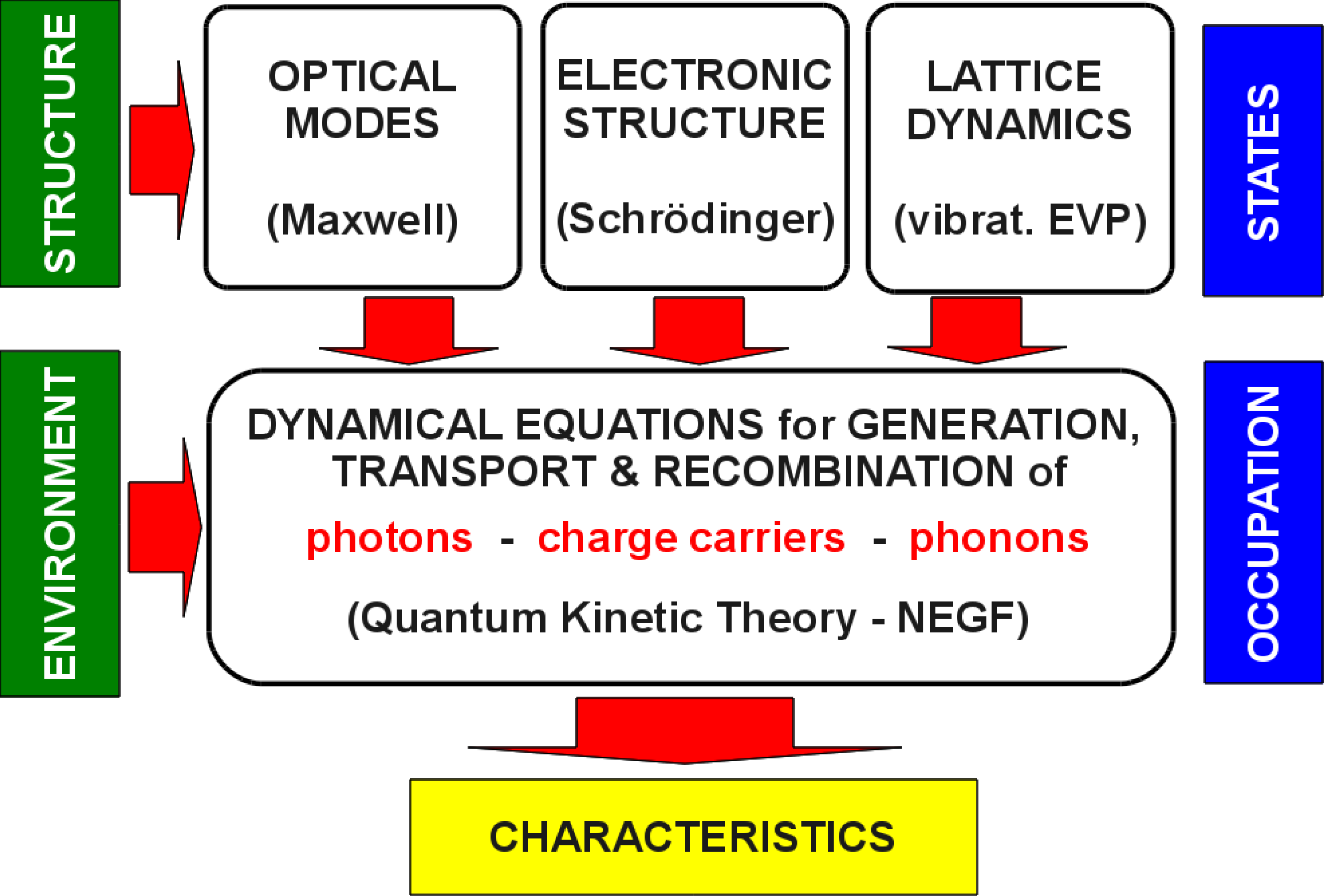
respectively. Similar expressions exist for the holes in terms of . As for the models based on the macroscopic transport equations, the computation of the Green’s functions needs to be coupled self-consistently to the determination of the electrostatic potential from Poisson’s equation, using the above expressions for the carrier densities in Eq. (7). Similar sets of equations can also be formulated for the optical and vibrational degrees of freedom (i.e., for photons and phonons), which then provides the desired comprehensive microscopic theory of NS-based optoelectronic devices (Fig. 5). For a more in-depth discussion of the NEGF formalism as applied to novel SC architectures, which is out of the scope of this review, the reader referred to [43] and references therein.
V Overview of existing modelling approaches
Here, we review the most relevant literature on theoretical descriptions and modelling approaches for specific types of NS-based high efficiency SC, with focus on models that consider not only a single step of the photovoltaic process, but which can actually be used to obtain the current-voltage characteristics - and with that the efficiency - of the device. This strongly reduces the amount of available literature in contrast to the huge number of papers on the optoelectronic properties of QW and QD systems.
V-A Multi-QW/QD solar cell
This type of SC comprises the approaches where NS extend the absorption range of the bulk device, but generated charge needs to escape to the bulk states in order to contribute to the photocurrent, such as, e.g., in the case of MQWSC or MQDSC111See [46] and [47] for a more extensive discussion of the physical foundations, theoretical description and numerical simulation of QWSC..
V-A1 Thermodynamic models and ideal theories
The earliest models for the MQWSC were thermodynamical theories of ideal devices. The original Shockley-Queisser formalism for single junction bulk devices was extended by Henry [48] to the case of multiple band gaps. The detailed balance approach of Corkish and Green [17] treated the QW as an incremental cell in addition to the baseline high bandgap bulk cell, but without any coupling between the two and in a field-free limit. and where then obtained from the superposition of baseline and incremental cell. Araújo and Martí [18] generalized the detailed balance analysis further, taking into account the light path in the device, variation of refractive indices and the angular range of incident and emitted radiation, and showing that for constant quasi-Fermi level separation (QFLS), the emissivity equals the absorptivity, with the consequence that within this limit, QWSC could not exceed the efficiency of an ideal homojunction device. The model of Bremner, Honsberg and Corkish [49], based on ideas proposed by Kettemann and Guillemoles [50], allowed for QFLS variations under assumption of radiative transitions between the different levels, which yields considerable efficiency increase, but might not be applicable to the case of QWSC, due to the very small intraband transition matrix elements for in-plane polarization. The origin of the variation in QFLS is not contained in the model, i.e. the QFLS-step is not an emergent feature of the theory. A simple and intuitive ideal QWSC model was presented by Anderson [19]: his approach, which in philosophy is similar to the model of Corkish and Green [17], is based on the ideal diode current-voltage characteristics for bulk homojunctions, with the quantum well material accounted for by enhancement factors for oscillator strength and DOS, providing the modifications of generation and recombination. However, the effects of QWs on the transport properties are not considered. This model was further developed by different authors [51, 52, 53, 54], including interface recombination and a better description of the QW absorption, to the point where it could be used to fit experimental data.
V-A2 Macroscopic continuum and hybrid transport models
The first quantitative theory for a MQWSC beyond thermodynamical and detailed balance approaches was developed by the group at Imperial College in the years after the first experimental implementation of the concept, and consists of a model for the escape of photogenerated carriers from QW [55], a semi-analytical model for the entire spectral response [31], and a numerical model for the dark current [56], with further improvements made in [57]. In the approach, whose early stages are summarized in [58], dark currents are obtained by analytical or numerical solution of the electron and hole drift-diffusion equations including the terms for generation and recombination and the coupling to Poisson’s equation. The carrier density is expressed in terms of the corresponding quasi-Fermi levels that are obtained from the transport equations, and which are assumed to be conserved across the interface between barrier and well material. In the case of QW, the expression for the density is modified by an additional factor to adjust to the two-dimensional DOS calculated from the solution of the effective mass equations in the envelope-function approximation [59] providing the subband energies. To include nonparabolicity of the light-hole band, a 4-band Kane model of the valence band is converted into corresponding 1D effective mass equations for each carrier-type, with the effective mass acquiring an energy dependence. The equations are solved numerically using a transfer-matrix method, which in addition provides the transmission function of the confining barrier. The DOS calculated in this way is also used to obtain the QW absorption that provide the generation rate. Excitonic contributions to absorption are included via parametric models with dimensionality parameters for exciton binding energies and oscillator strengths; the parameters are obtained from a fit to the solution of the effective mass equation for excitons. The absolute excitonic absorption is scaled and convolved with a Lorentzian for homogeneous broadening to fit the experimental data. Layer widths, composition and doping levels are determined from growth record and characterization studies, and the minority carrier diffusion lengths are calculated from layer doping and alloy fraction. The recombination rates are determined by the bulk and QW densities and the recombination times including radiative, SRH and Auger recombination, are obtained from fits to the corresponding bulk control cell dark currents. The escape lifetime model describing carrier escape from QW includes thermionic emission and (thermally assisted) tunneling. The lifetime is derived from the escape current, which in turn is determined by the carrier density at a fixed energy, given by the DOS and the occupation, and the transmission function of the confining barrier at that energy. At room temperature and moderate fields, the probability of escape from QWs in the intrinsic region is set to unity, in accordance with carrier escape experiments [55]. The models were eventually combined by Conolly [60] to a comprehensive modelling approach for QWSC, using a simplified approach for the dark current and assuming unit escape efficiency.
In spite of its comprehensiveness, there are several shortcomings in the approach, which in the reproduction of experimental characteristics are in part compensated by adjusting a number of fitting parameters. Most notably, the description of quasi-bound states close to the top of the well is poor, since near the top of the wells, the envelope-function approximation breaks down, and the QW-DOS gradually becomes bulk-like, which is not reflected in the model. While absorption and emission are primarily dominated by the states close to the effective band edge. i.e., deep in the well, these high-lying states play a decisive role in the escape and capture of carriers. Furthermore, the DOS and correspondingly the absorption above the wells is assumed to be that of homogeneous bulk, which is not the case due to the existence of quasi-bound states and higher resonances. The assumption of unit escape breaks down for deeper wells, and capture processes are not considered explicitely in the model. The model in its standard formulation does also not include the effects of finite fields across the QWs, which lead to hybridization of QW and bulk states, a shift of confinement levels (quantum confied Stark effect) and modified absorption due to decreased overlap of asymmetric electron and hole wave functions. A further drawback is the requirement for the assumption of constant QFL separation in wells and barriers, which might not hold in all cases, as indicated by experimental observations [61] and numerical investigations with spatially varying QFLS [62, 63].
Apart from the work by the Imperial College group, further modelling efforts include the model of Varonides [64], which explicitly takes into account thermionic emission and tunneling in a way very similar to Nelson [55], but tunneling is restricted to the triangular barrier of an isolated well. A more comprehensive self-consistent Schrödinger-Poisson-drift-diffusion model for carrier generation, recombination and transport in QWSC was developed by Ramey and Khoie [37]. In distinction to the above modelling framework, this approach describes also carrier capture into QW, solving separate equations for densities of carriers in localized and extended states, and the escape model considers the 2D-DOS, the subband energy level structure including valence-band mixing and escape from direct and indirect valleys, and the field and temperature dependence, but neglects tunneling escape, since it is assumed to be suppressed at room temperatures and low fields. The QW-absorption is obtained from a semiempirical model [65], not considering excitons, bandstructure or field effects, and only non-radiative recombination (SRH) is described. A more recent approach by Kailuweit et al. [66] uses a commercial device simulator for the transport, where barrier and well regions are treated as bulk materials (implicitly assuming unit escape probability), together with the QW absorption model introduced in [31]. For MQDSC, a simple semi-analytical model in the spirit of Paxman [31] is presented by Aroutiounian et al. in [67] and extended later by the same authors to include emission and capture rates [68].
While the models reviewed so far did not consider the (resonant) coupling of multiple quantum wells (while still extracting carriers via the states of the bulk host), which can significantly enhance carrier escape [69], the inclusion of (coherent) multi-barrier tunneling into the analysis of QWSC performance was accounted for in the model by Mohaidat et al. [70], in which a numerical solution of the time dependent Schrödinger equation is used to calculate resonant tunneling transport of photogenerated carriers in MQW with thin barriers. However, the model was never embedded into a more comprehensive picture including explicitly carrier generation, recombination and escape channels other than via tunneling.
V-A3 Mesoscopic quantum-kinetic approaches
As mentioned above, the assumption of unit thermal escape efficiency starts to break down for deep or strongly coupled QW. The necessary inclusion of alternative escape channels requires consideration of the actual non-equilibrium occupation of quasi-bound states as established under illumination and bias, which is beyond the capabilities of the hybrid approach. The formulation of a comprehensive quantum-kinetic theory for QWSC by Aeberhard and Morf [71, 72, 73, 74], based on the non-equilibrium Green’s function formalism, allowed for the first time for a consistent description of carrier photogeneration, escape, capture and radiative recombination mediated by states of arbitrary degree of localization resulting from realistic potential profiles and under arbitrary non-equilibrium conditions. As the approach does not rely on local quasi-Fermi levels, it does not make any assumptions on the equilibration between nanostructure and bulk host states. In the description of escape and capture processes, transport at any energy is considered, covering both coherent and phonon-assisted tunneling contributions. However, due to the considerable numerical cost of the approach, only simple effective mass or few-band tight-binding models were used for the electronic structure, and characteristics could only be obtained for structures of mesoscopic spatial extension.
V-B QW/QD-superlattice solar cell
This category of solar cell comprises any concept based on miniband transport, e.g., by QW or QD superlattices, often proposed as tunable absorber components in multi-junction architectures. A basic ingredient of most models is the miniband structure associated with delocalized superlattice states. For QWSL, approaches ranging from simple transfer matrix formalisms [75] to advanced ab-initio methods [76] have been used for this purpose. For QDSL, a popular procedure consists in the superposition of solutions to the 1D Kronig-Penney model for a single band effective mass Hamiltonian [33], based on [77]. While the absorption (and, via detailed balance, the radiative dark current) is determined in many cases from the computed electronic structure, the latter does either not enter the transport problem at all [75, 78], or only via an effective density of states and a so-called Bloch mobility [76] derived from the curvature in transport direction of the miniband for the perfect superlattice in the absence of disorder and fields, together with an effective scattering lifetime [33]. Photogeneration and photocarrier transport for more realistic situations concerning internal fields and inelastic scattering processes (electron-phonon interaction) were investigated using the quantum-kinetic approach in [79] for Si-SiOx QWSL absorbers, confirming the detrimental effect of high barriers on mobility and of thin barriers on confinement, and in [80] for Si-SiC-SiOx QDSL solar cells, revealing strong QD wave function localization already in moderate built-in fields.
VI Remaining challenges and open problems
The NS-based implementations of novel high efficiency solar cell concepts are of similar complexity as state-of-the-art devices in nanoelectronics and solid-state lighting. However, advanced theoretical concepts for electron transport at the nanoscale are only slowly being adopted to simulate nanostructure-based solar cells, although such concepts are, for example, readily applied in the simulation of solid-state lighting”. This is in part due to the problem of scales: even under application of advanced light-trapping schemes, the thickness required to absorb a substantial fraction of the incident light is still of the order of a few hundred nm, which is beyond the capabilities of any model with atomistic resolution, especially in the case of irregular, non-periodic arrangements of NS exhibiting 3D confinement, such as realistic QD arrays. The development of adequate forms of multi-scale modelling[81], ranging from parametrization of effective Hamiltonians from first-principles to the derivation of current- and charge-conserving interface conditions between micro- and macroscopic transport models, will thus be a major focus in future research on simulation models for PV devices based on NS. Due to the impact of nanoscale size on any kind of physical properties of the NS-based device on the one hand, and the nature of the solar cell as an optoelectronic device operating at elevated temperatures on the other hand, the multi-scale aspect is accompanied by the notion of a multi-physics approach that is required for an adequate description of the device operation, i.e., including transport of charge, light and heat at all scales.
Concerning the mesoscopic quantum-kinetic ingredient to the modelling framework, defect-mediated processes and advanced electron-electron scattering mechanisms required to describe impact-ionization, Auger recombination or hot-electron distributions are still awaiting implementation. In some cases of strong coupling, the single-particle picture may no longer be appropriate, and quasi-particles such as excitons, polarons, plasmons or polaritons should be considered. Finally, in realistic devices, an additional challenge arises from the presence of disordered materials such as amorphous phases, e.g., in embedding matrix components, which requires tedious configuration averages in order to extract representative device characteristics.
VII Conclusions
In this paper, theoretical approaches for the simulation of NS-based high-efficiency solar cell devices have been reviewed, with focus on solar cells based on QW and QD absorbers with varying degree of coupling between the NS components. In many cases, the effects of quantum confinement on optical, electronic and vibrational properties of the NS interdicts the use of conventional bulk approaches. While the optical properties can be considered by explicitly computing the absorption coefficient from the modified electronic structure and applying the principle of detailed balance for the emission, the inclusion of the effects on transport and non-radiative recombination requires a careful consideration of the microscopic mechanisms that couple NS and bulk host states. If both tunneling and scattering processes are essential for the device operation, as in the case of strongly coupled NS subject to significant electric fields, an adequate description of photocarrier generation and extraction requires the use of advanced microscopic quantum-kinetic approaches. Due to the huge computational cost of the latter, future approaches should aim at a combination of mesoscopic quantum-kinetic descriptions for the NS components and a macroscopic picture for the bulk regions in a general multi-scale and multi-physics modelling framework.
References
- [1] W. Shockley and H. J. Queisser, “Detailed balance limit of efficiency of p-n junction solar cells,” J. Appl. Phys., vol. 32, no. 3, pp. 510–519, 1961.
- [2] A. Martí, Next generation photovoltaics : high efficiency through full spectrum utilization, ser. Series in optics and optoelectronics. Bristol: IOP, 2004.
- [3] M. A. Green, Third Generation Photovoltaics Advanced Solar Energy Conversion. Berlin, Heidelberg: Springer-Verlag Berlin Heidelberg,, 2006.
- [4] M. Yamaguchi, T. Takamoto, K. Araki, and N. Ekins-Daukes, “Multi-junction III-V solar cells: current status and future potential,” Sol. Energy, vol. 79, p. 78, 2005.
- [5] A. Luque and A. Martí, “Increasing the efficiency of ideal solar cells by photon induced transitions at intermediate levels,” Phys. Rev. Lett., vol. 78, no. 26, pp. 5014–5017, Jun 1997.
- [6] A. J. Nozik, “Exciton multiplication and relaxation dynamics in quantum dots: applications to ultrahigh-efficiency solar photon conversion,” Inorg. Chem., vol. 44, no. 20, pp. 6893–6899, 2005.
- [7] R. T. Ross and A. J. Nozik, “Efficiency of hot-carrier solar energy converters,” J. Appl. Phys., vol. 53, no. 5, pp. 3813–3818, 1982.
- [8] L. Tsakalakos, “Nanostructures for photovoltaics,” Mater. Sci. Eng., R, vol. 62, no. 6, pp. 175 – 189, 2008.
- [9] H. A. Atwater and A. Polman, “Plasmonics for improved photovoltaic devices,” Nat. Mater., vol. 9, no. 3, pp. 205–213, 2010.
- [10] S. Mokkapati and K. R. Catchpole, “Nanophotonic light trapping in solar cells,” J. Appl. Phys, vol. 112, no. 10, p. 101101, 2012.
- [11] L.-W. Wang, “Computational challenges for nanostructure solar cells,” Energy Environ. Sci., vol. 2, no. 9, pp. 944–955, 2009.
- [12] Y. Kanai, J. Neaton, and J. Grossman, “Theory and simulation of nanostructured materials for photovoltaic applications,” Comput. Sci. Eng., vol. 12, no. 2, pp. 18–27, 2010.
- [13] M. W. Wanlus and A. E. Blakeslee, “Superlattice cascade solar cell,” in Conf. Record, 16th IEEE Photovoltaic Specialists Conference, San Diego, CA, 1982, p. 584.
- [14] R. Chaffin, G. Osbourn, L. Dawson, and R. Biefeld, “Strained superlattice, quantum well, multijunction photovoltaic cell,” in Conf. Record, 17th IEEE Photovoltaic Specialists Conference, Kissimmee, 1984, p. 743.
- [15] K. W. J. Barnham, B. Braun, J. Nelson, M. Paxman, C. Button, J. S. Roberts, and C. T. Foxon, “Short-circuit current and energy efficiency enhancement in a low-dimensional structure photovoltaic device,” Appl. Phys. Lett., vol. 59, no. 1, pp. 135–137, 1991.
- [16] M. A. Green, “Potential for low dimensional structures in photovoltaics,” J. Mater. Sci. Eng. B, vol. 74, no. 1-3, pp. 118 – 124, 2000.
- [17] R. Corkish and M. Green, “Recombination of carriers in quantum well solar cells,” in Conference Record of the Twenty Third IEEE Photovoltaic Specialists Conference, 1993, p. 675.
- [18] G. Araújo, A. Martí, F. Ragay, and J. Wolter, “Efficiency of multiple quantum well solar cells,” in Proc. 12th European Photovoltaic Solar Energy Conference, 1994, p. 1481.
- [19] N. Anderson, “Ideal theory of quantum well solar cells,” J. Appl. Phys., vol. 78, p. 1861, 1995.
- [20] N. J. Ekins-Daukes, D. B. Bushnell, J. Connolly, K. W. J. Barnham, M. Mazzer, J. S. Roberts, G. Hill, and R. Airey, “Strain-balanced quantum well solar cells,” Physica E, vol. 14, p. 132, 2002.
- [21] J. G. J. Adams, W. Elder, G. Hill, J. S. Roberts, K. W. J. Barnham, and N. J. Ekins-Daukes, “Higher limiting efficiencies for nanostructured solar cells,” in Proceedings of SPIE - The International Society for Optical Engineering, vol. 7597, 2010.
- [22] S. M. Hubbard, C. D. Cress, C. G. Bailey, R. P. Raffaelle, S. G. Bailey, and D. M. Wilt, “Effect of strain compensation on quantum dot enhanced gaas solar cells,” Appl. Phys. Lett., vol. 92, no. 12, p. 123512, Mar. 2008.
- [23] R. Oshima, A. Takata, and Y. Okada, “Strain-compensated InAs/GaNAs quantum dots for use in high-efficiency solar cells,” Appl. Phys. Lett., vol. 93, no. 8, p. 083111, Aug. 2008.
- [24] M. A. Green, K. Emery, Y. Hishikawa, W. Warta, and E. D. Dunlop, “Solar cell efficiency tables (version 41),” Prog. Photovolt.: Res. Appl., vol. 21, no. 1, pp. 1–11, 2013.
- [25] G. Conibeer and M. Green, “Phononic band gap engineering for hot carrier solar cell absorbers,” in Proceedings of the 21st EUPVSEC, Dresden, 2006.
- [26] G. Conibeer, M. Green, E. . Cho, D. König, Y. . Cho, T. Fangsuwannarak, G. Scardera, E. Pink, Y. Huang, T. Puzzer, S. Huang, D. Song, C. Flynn, S. Park, X. Hao, and D. Mansfield, “Silicon quantum dot nanostructures for tandem photovoltaic cells,” Thin Solid Films, vol. 516, no. 20, pp. 6748–6756, 2008
- [27] G. Allan and C. Delerue, “Efficient intraband optical transitions in Si nanocrystals,” Phys. Rev. B, vol. 66, no. 23, p. 233303, Dec 2002.
- [28] J.-W. Luo, P. Stradins, and A. Zunger, “Matrix-embedded silicon quantum dots for photovoltaic applications: a theoretical study of critical factors,” Energy Environ. Sci., vol. 4, pp. 2546–2557, 2011.
- [29] J.-M. Wagner, K. Seino, F. Bechstedt, A. Dymiati, J. Mayer, R. Rölver, M. Först, B. Berghoff, B. Spangenberg, and H. Kurz, “Electronic band gap of Si/SiO2 quantum wells: Comparison of ab initio calculations and photoluminescence measurements,” J. Vac. Sci. Technol. A, vol. 25, no. 6, pp. 1500–1504, 2007.
- [30] M. Zacharias, J. Heitmann, R. Scholz, U. Kahler, M. Schmidt, and J. Bläsing, “Size-controlled highly luminescent silicon nanocrystals: A SiO/SiO2 superlattice approach,” Appl. Phys. Lett., vol. 80, no. 4, pp. 661–663, 2002.
- [31] M. Paxman, J. Nelson, B. Braun, J. Connolly, K. W. J. Barnham, C. T. Foxon, and J. S. Roberts, “Modeling the spectral response of the quantum well solar cell,” J. Appl. Phys, vol. 74, p. 614, 1993.
- [32] A. Wacker, “Semiconductor superlattices: a model system for nonlinear transport,” Phys. Rep., vol. 357, p. 1, 2002.
- [33] C.-W. Jiang and M. A. Green, “Silicon quantum dot superlattices: Modeling of energy bands, densities of states, and mobilities for silicon tandem solar cell applications,” J. Appl. Phys., vol. 99, no. 11, p. 114902, 2006.
- [34] N. J. Ekins-Daukes, K. W. J. Barnham, J. P. Connolly, J. S. Roberts, J. C. Clark, G. Hill, and M. Mazzer, “Strain-balanced GaAsP/InGaAs quantum well solar cells,” Appl. Phys. Lett., vol. 75, no. 26, pp. 4195–4197, 1999.
- [35] K. Ding, U. Aeberhard, O. Astakhov, U. Breuer, M. Beigmohamadi, S. Suckow, B. Berghoff, W. Beyer, F. Finger, R. Carius, and U. Rau, “Defect passivation by hydrogen reincorporation for silicon quantum dots in SiC/SiOx hetero-superlattice,” J. Non-Cryst. Solids, no. 0, pp. –, 2012.
- [36] W. V. Roosbroeck and W. Shockley, “Photon-radiative recombination of electrons and holes in germanium,” Phys. Rev., vol. 94, p. 1558, 1954.
- [37] R. Ramey and R. Khoie, “Modeling of multiple-quantum-well solar cells including capture, escape, and recombination of photoexcited carriers in quantum wells,” IEEE Trans. Electron Devices, vol. 50, p. 1179, 2003.
- [38] S. Datta, Electronic Transport in Mesoscopic Systems. Cambridge University Press, 1995.
- [39] ——, Quantum Transport. Cambridge University Press, 2005.
- [40] H. Haug and A. P. Jauho, Quantum kinetics in transport and optics of semiconductors. Springer, Berlin, 1996.
- [41] W. Schäfer and M. Wegener, Semiconductor Optics and Transport Phenomena. Springer, Berlin, 2002.
- [42] H. Haug and S. W. Koch, Quantum Theory of the Optical and Electronic Properties of Semiconductors. World Scientific, 2004.
- [43] U. Aeberhard, “Theory and simulation of quantum photovoltaic devices based on the non-equilibrium green’s function formalism,” J. Comput. Electron., vol. 10, pp. 394–413, 2011.
- [44] L. P. Kadanoff and G. Baym, Quantum Statistical Mechanics. Benjamin, Reading, Mass., 1962.
- [45] L. Keldysh, “Diagram technique for nonequilibrium processes,” Sov. Phys. JETP, vol. 20, p. 1018, 1965.
- [46] U. Aeberhard, “A Microscopic Theory of Quantum Well Photovoltaics,” Ph.D. dissertation, ETH Zurich, 2008.
- [47] U. Aeberhard and R. Morf, Photovoltaic effects in quantum confined systems: microscopic theory and numerical simulation, V. Badescu and M. Paulescu, Eds. Nova Science, 2010.
- [48] C. Henry, “Limiting efficiencies of ideal single and multiple energy gap terrestrial solar cells,” J. Appl. Phys., vol. 51, p. 4494, 1980.
- [49] S. Bremner, R. Corkish, and C. Honsberg, “Detailed balance efficiency limits with quasi-fermi level variations,” IEEE Trans. Electron Devices, vol. 46, no. 10, pp. 1932–1939, 1999.
- [50] S. Kettemann and J. Guillemoles, in Proceedings of the 13th European Photovoltaic Solar Energy Conference, 1995.
- [51] J. Rimada and L. Hernández, “Modelling of ideal algaas quantum well solar cells,” Microelectron. J., vol. 32, no. 9, pp. 719 – 723, 2001.
- [52] S. J. Lade and A. Zahedi, “A revised ideal model for algaas/gaas quantum well solar cells,” Microelectron. J., vol. 35, no. 5, pp. 401–410, May 2004.
- [53] J. C. Rimada, L. Hernández, J. P. Connolly, and K. W. J. Barnham, “Quantum and conversion efficiency calculation of algaas/gaas multiple quantum well solar cells,” Phys. Stat. Sol. B, vol. 242, no. 9, pp. 1842–1845, Jul. 2005.
- [54] ——, “Conversion efficiency enhancement of algaas quantum well solar cells,” Microelectron. J., vol. 38, no. 4-5, pp. 513–518, Apr. 2007.
- [55] J. Nelson, M. Paxman, K. W. J. Barnham, J. Roberts, and C. Button, “Steady state carrier escape rates from single quantum wells,” IEEE J. Quantum Electron., vol. 29, p. 1460, 1993.
- [56] J. Nelson, K. W. J. Barnham, J. P. Connolly, G. Haarpaintner, C. Button, and J. Roberts, “Quantum well solar cell dark currents,” in Proc. 12th EU PVSEC, 1994.
- [57] J. Nelson, I. Ballard, K. Barnham, J. P. Connolly, J. S. Roberts, and M. Pate, “Effect of quantum well location on single quantum well p-i-n photodiode dark currents,” J. Appl. Phys, vol. 86, p. 5898, 1999.
- [58] J. Nelson, “Quantum-well structures for photovoltaic energy conversion,” Thin Films, vol. 21, p. 311, 1995.
- [59] G. Bastard and J. Brum, “Electronic states in semiconductor heterostructures,” IEEE J. Quantum Electron., vol. 22, no. 9, pp. 1625–1644, 1986.
- [60] J. P. Connolly, J. Nelson, K. W. Barnham, I. Ballard, C.Roberts, J. Roberts, and C.T.Foxon, “Simulating multiple quantum well solar cells,” in Proc. 28th IEEE Photovoltaic Specialists Conference, 2000, p. 1304.
- [61] J. Nelson, J. Barnes, N. Ekins-Daukes, B. Kluftinger, E. Tsui, K. Barnham, C. T. Foxon, and T. Cheng, “Observation of suppressed radiative recombination in single quantum well p-i -n photodiodes,” J. Appl. Phys., vol. 82, p. 6240, 1997.
- [62] R. Corkish and C. B. Honsberg, “Dark currents in double-heterostructure and quantum-well solar cells,” in Photovoltaic Specialists Conference, 1997., Conference Record of the Twenty-Sixth IEEE, 1997.
- [63] S. Bremner, R. Corkish, and C. Honsberg, “Detailed balance efficiency limits with quasi-Fermi level variations,” IEEE Trans. Electron Devices, vol. 46, p. 1932, 1999.
- [64] A. C. Varonides, “Thermionic escape of net photogenerated carriers and current densities from illuminated lightly doped single quantum wells,” Physica E, vol. 14, p. 142, 2002.
- [65] G. Lengyel, K. Jelley, and R. Engelmann, “A semi-empirical model for electroabsorption in GaAs/AlGaAs multiple quantum well modulator structures,” IEEE J. Quantum Electron., vol. 26, no. 2, pp. 296–304, 1990.
- [66] P. Kailuweit, R. Kellenbenz, S. P. Philipps, W. Guter, A. W. Bett, and F. Dimroth, “Numerical simulation and modeling of GaAs quantum-well solar cells,” J. Appl. Phys., vol. 107, no. 6, p. 064317, 2010.
- [67] V. Aroutiounian, S. Petrosyan, A. Khachatryan, and K. Touryan, “Quantum dot solar cells,” J. Appl. Phys., vol. 89, no. 4, pp. 2268–2271, Feb. 2001.
- [68] V. Aroutiounian, S. Petrosyan, and A. Khachatryan, “Studies of the photocurrent in quantum dot solar cells by the application of a new theoretical model,” Sol. Energy Mater. Sol. Cells, vol. 89, no. 2-3, pp. 165–173, Nov. 2005.
- [69] A. Zachariou, J. Barnes, K. W. J. Barnham, J. Nelson, E. S. M. Tsui, J. Epler, and M. Pate, “A carrier escape study from InP/InGaAs single quantum well solar cells,” J. Appl. Phys., vol. 83, p. 881, 1998.
- [70] J. M. Mohaidat, K. Shum, W. B. Wang, and R. R. Alfano, “Barrier potential design criteria in multiple-quantum-well-based solar-cell structures,” J. Appl. Phys., vol. 76, p. 5533, 1994.
- [71] U. Aeberhard and R. H. Morf, “Microscopic nonequilibrium theory of quantum well solar cells,” Phys. Rev. B, vol. 77, p. 125343, 2008.
- [72] U. Aeberhard and U. Rau, “Microscopic theory of absorption and emission in nanostructured solar cells: Beyond the generalized planck formula,” in Proc. of the 24th EU PVSEC,Hamburg, 2009.
- [73] U. Aeberhard, “Spectral properties of photogenerated carriers in quantum well solar cells,” Sol. Energy Mater. Sol. Cells, vol. 94, no. 11, pp. 1897 – 1902, 2010, inorganic and Nanostructured Photovoltaics.
- [74] ——, “Microscopic theory and numerical simulation of quantum well solar cells,” B. Witzigmann, F. Henneberger, Y. Arakawa, and M. Osinski, Eds., vol. 7597, no. 1. SPIE, 2010, p. 759702.
- [75] M. Courel, J. C. Rimada, and L. Hernández, “GaAs/GaInNAs quantum well and superlattice solar cell,” Appl. Phys. Lett., vol. 100, no. 7, p. 073508, 2012.
- [76] T. Kirchartz, K. Seino, J.-M. Wagner, U. Rau, and F. Bechstedt, “Efficiency limits of Si/SiO2 quantum well solar cells from first-principles calculations,” J. Appl. Phys., vol. 105, no. 10, p. 104511, 2009.
- [77] O. L. Lazarenkova and A. A. Balandin, “Miniband formation in a quantum dot crystal,” J. Appl. Phys., vol. 89, no. 10, pp. 5509–5515, 2001.
- [78] M. Courel, J. C. Rimada, and L. Hernandez, “An approach to high efficiencies using GaAs/GaInNAs multiple quantum well and superlattice solar cell,” J. Appl. Phys., vol. 112, no. 5, p. 054511, Sep. 2012.
- [79] U. Aeberhard, “Theory and simulation of photogeneration and transport in Si-SiOx superlattice absorbers,” Nanoscale Res. Lett., vol. 6, p. 242, 2011.
- [80] ——, “Effective microscopic theory of quantum dot superlattice solar cells,” Opt. Quantum. Electron., vol. 44, pp. 133–140, 2012.
- [81] M. Auf Der Maur, G. Penazzi, G. Romano, F. Sacconi, A. Pecchia, and A. Di Carlo, “The multiscale paradigm in electronic device simulation,” IEEE Trans. Electron. Devices, vol. 58, no. 5, pp. 1425–1432, 2011.
![[Uncaptioned image]](/html/1304.1957/assets/x11.png) |
Urs Aeberhard obtained his PhD in physics from ETH Zürich, Switzerland, in 2008 with a thesis on the quantum-kinetic theory of quantum-well solar cell devices, carried out in the Condensed Matter Theory Group at Paul Scherrer Institute under the supervision of Dr. Rudolf Morf. From 2009-2012, he was a postdoctoral researcher at the Institute of Energy and Climate Research 5 - Photovoltaics at Forschungszentrum Jülich, Germany, where he is now leading the activities in theoretical materials science and microscopic device simulation. The focus of his research is on the development of theory and numerical simulations for advanced nanostructure-based solar cell devices. |