Trapping hot quasi-particles in a high-power superconducting electronic cooler
Abstract
The performance of hybrid superconducting electronic coolers is usually limited by the accumulation of hot quasi-particles in their superconducting leads. This issue is all the more stringent in large-scale and high-power devices, as required by applications. Introducing a metallic drain connected to the superconducting electrodes via a fine-tuned tunnel barrier, we efficiently remove quasi-particles and obtain electronic cooling from 300 mK down to 130 mK with a 400 pW cooling power. A simple thermal model accounts for the experimental observations.
Introduction
On-chip solid-state refrigeration has long been sought for various applications in the sub-kelvin temperature regime, such as cooling astronomical detectors [1, 2, 3]. In a Normal metal - Insulator - Superconductor (NIS) junction [4, 5, 6], the superconductor density of states gap makes that only high-energy electrons are allowed to tunnel out of the normal metal or, depending on the bias, low-energy ones to tunnel in, so that the electronic bath as a whole is cooled. In SINIS devices based on aluminum, the electronic temperature can drop from 300 mK down to below 100 mK at the optimum bias point. While this level of performance has been demonstrated in micron-scale devices [7, 8] with a cooling power in the picoWatt range, a difficulty arises in devices with large-area junctions needed for a sizable cooling power approaching the nanoWatt range. For instance, a high-power refrigerator has been shown to cool an external object from 290 mK down to about 250 mK [9]. One of the main limitation to NIS coolers’ full performance is the presence in the superconducting leads of non-equilibrium quasi-particles arising from the high current running through the device. The low quasi-particle relaxation rate and thermal conductivity in a superconductor bound these hot particles in the vicinity of the junction and lead to severe overheating in the superconducting electrodes.
There are several methods for reducing the accumulation of quasi-particles in a superconductor. For example a small magnetic field [10] can be used to introduce vortices that trap quasi-particles. This approach is however not applicable to electronic coolers with large-area junctions since a vortex also reduces the cooling performance if it resides within a junction. The most common method is to use a normal metal coupled to the superconductor as a quasi-particle trap: quasi-particles migrate to the normal metal and relax their energy there through electron-electron and electron-phonon interaction. In the typical case of a fabrication process based on angle evaporation, quasi-particle traps are formed by the structures mirroring each superconducting electrode, sitting on a side of the cooling junction and featuring the same oxide barrier layer. The trapping efficiency is usually moderate, but can be improved in two ways: the normal metal can be put in direct contact with the superconductor, as out-of-equilibrium quasi-particles would diffuse more efficiently to the trap [11], or the trap can be closer to the junction [12, 13]. In both cases, it is important to prevent inverse proximity effect in the superconductor, which smears locally the superconductor density of states and degrades cooling efficiency. The existence of an optimum transparency for the interface between the trap and the superconducting lead is therefore expected, but remains to be investigated [14].
In this paper, we present an effective method to evacuate quasi-particles in a SINIS cooler, based on what we call a quasi-particle drain. It is a kind of quasi-particle trap made of a layer of normal metal located at a fraction of superconducting coherence length away from the junction and separated by a thin insulating layer to stop the inverse proximity effect. We compare the cooling performance when varying the quasi-particle drain barrier transparency over a wide range. The efficiency of the quasi-particle drain is demonstrated through the electronic cooling from 300 to 130 mK at a 400 pW cooling power. A simple thermal model captures the effect of the quasi-particle drain reasonably well.
Fabrication and measurement methods
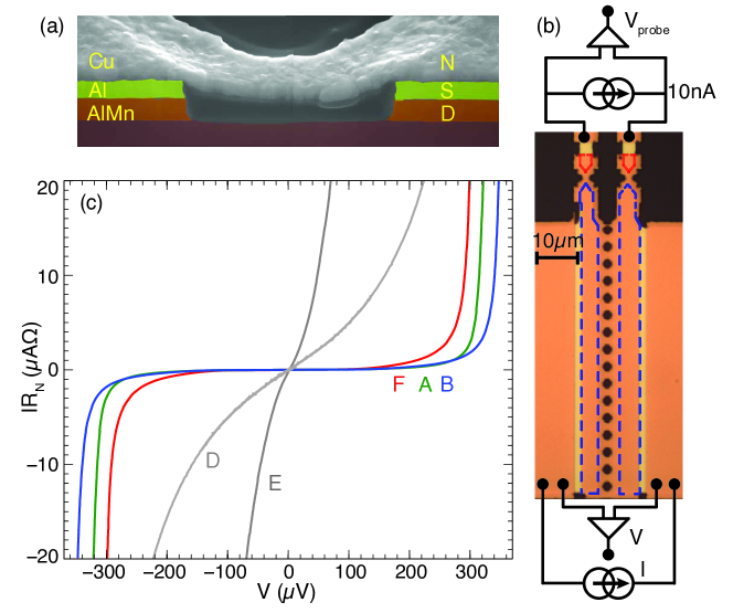
We use the fabrication process described in Ref. [15], in which a SINIS cooler is obtained by photo-lithography and chemical etch of a NIS multilayer. Here, we add a normal metal layer at the bottom, which is used as a quasi-particle drain. Figure 1a false-colored scanning electron micrograph shows a side view of a typical SINIS cooler, obtained by cutting it with a focused ion beam. From top to bottom, the 100 nm-thick Cu normal metal layer to be cooled is suspended between two 200 nm-thick Al superconducting electrodes. The latter rest on two separate quasi-particle drains made of a 200 nm layer of AlMn deposited on a Si wafer. We choose AlMn [16, 17] as a quasi-particle drain normal material because it acts chemically as Al in terms of oxidation and etch. The layers are separated by two aluminum oxide barriers, which we name the drain barrier between the AlMn and Al layers and the cooler barrier between the Al and Cu layers. Sample parameters are given in Table 1.
-
Sample Drain barrier Cooler barrier Color (mbar, second) (mbar, second) A 1.3, 10 1.3, 300 0.71 398 green B 0.26, 10 1.3, 300 1.56 382 blue C 0.18, 1 0.8, 180 0.55 370 purple D 510-4, 10 1.3, 300 1.01 228 gray E 0 1.3, 180 1.31 180 gray F N/A 1, 300 0.83 390 red
Figure 1b is an optical micrograph showing a top view of the cooler. The two NIS junctions area are outlined by dashed blue lines. They are separated by a trench in the Al and AlMn layers, created by chemical over-etch, underneath the array of holes in the suspended Cu layer. Each junction has an area of 70 4 m2 and is surrounded by two quasi-particle traps: a side trap made of Cu next to it, and a quasi-particle drain made of AlMn. Two additional small NIS junctions connected to the normal metal are used as a SINIS thermometer. Electron temperature is accessed by comparing the measured voltage drop under a small bias current (typically 10 nA) to a calibration against the cryostat temperature.
Experimental results and discussion
The current flowing through a NIS junction with a voltage V writes
| (1) |
where is the normalized superconductor density of states, is the superconducting gap, is the normal state junction resistance, and are the Fermi-Dirac energy distributions of electrons in S and N, respectively. If leakage is negligible, a low sub-gap current then means a low electronic temperature.
Figure 1c shows the current voltage characteristics (IV curves) of different samples measured with a standard current-biased 4-probe technique in a dilution cryostat at 50 mK, with a focus on the low-bias regime. The two innermost curves stand for samples E and D, which have no drain barrier and a very thin drain barrier, respectively. Superconductivity in the Al layers is then affected by a strong inverse proximity effect, which results in a depressed critical temperature and a low superconducting gap so that = 180 eV and 228 eV respectively.
As samples A, B, and C are fabricated using a higher oxidation pressure for the drain barrier, they have a typical value for of about 350 eV and a ratio of minimum conductance to normal-state conductance of about , indicating that inverse proximity effect is weak. These samples show a sharp IV characteristic, with sample C (not shown) behaving almost identically to sample B. The sole difference between samples A and B is the drain barrier. Having a thinner barrier, sample B exhibits less current at a given sub-gap bias, i.e. less overheating from quasi-particles in the superconductor. The drain barrier lets quasi-particles get efficiently trapped in the drain, while it stops the inverse proximity effect.
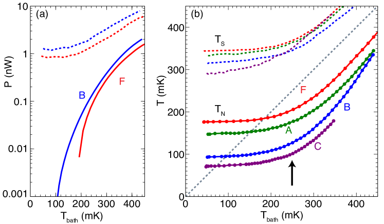
In a normal metal, the main heat flux from the electron system to the environment is through the coupling with the phonon system. We estimate the cooling power from the electron-phonon coupling power using
| (2) |
where WK-5m-3 is the electron-phonon coupling constant in Cu [18, 19], m3 is the island volume for all samples, is the measured electron temperature and is the phonon temperature, both in the normal island. We assume here that , which leads to an upper limit on the estimation of the cooling power. Figure 2a displays the calculated electron-phonon coupling power (solid lines) and the total Joule power (dashed lines) measured at the optimum bias, i.e. the bias at which electronic cooling is maximum. The typical power scale for all our present coolers is in the nanoWatt range.
Figure 2 b presents the most important result of our work, namely the behavior of the normal island electronic temperature at optimum bias as a function of the bath temperature. All coolers have the largest temperature drop at a bath temperature around 300 mK. At lower temperatures, heating above the bath temperature is observed, which arises from the sub-gap current. Having only the side trap and no quasi-particle drain, sample F shows a poor cooling from 300 mK down to only 230 mK. Carrying a quasi-particle drain, sample A cools to 200 mK. With a reduced drain barrier, sample B cools to 160 mK. In sample C, we obtain the best cooling by further reducing the drain and the cooler barriers: from 300 mK, sample C cools down to 132 mK with a 400 pW cooling power. Most importantly, from a bath temperature of 250 mK, sample C cools down to below 100 mK, see the arrow in Fig. 2b.
The electronic temperature of the superconducting electrodes can be accessed by balancing the normal metal electron-phonon coupling power (Eq. 2) with the NIS junction cooling power at a voltage bias :
| (3) |
Figure 2 b upper part (dashed lines) displays the electronic temperature of the superconductor derived when assuming again in the normal metal. Although the latter assumption calls for further discussion, the trend remains that the superconductor gets significantly overheated.
Thermal model
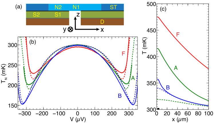
In order to describe further the thermal transport in our devices, we consider a one-dimensional multilayered thermal model. It is a set of coupled heat equations for different systems. The model geometry shown in figure 3a includes a normal metal island (N), superconducting leads (S), side traps (ST), and quasi-particle drains (D), similar to the geometry of the studied coolers (figure 1a). Although a non-equilibrium description of a biased NIS junction is possible [20, 21], we assume for simplicity every part of the device can be described by local temperature. We also neglect inverse proximity effect in the superconductor density of electronic states, as can be justified by the sharpness of measured IVs.
In the following equations, we will make use of the quantities , and that are the local current , cooling power and electron-phonon coupling power per unit area in the plane, see Fig. 3a. In addition, is the temperature, is the thickness and is the thermal conductivity in the element . Here, temperature gradients are in the -direction, charge and heat currents through the junctions ( and ) are in the -direction, electron-phonon couplings are in the bulk. In the normal metal, the temperature gradient is determined by the electronic thermal conductivity, the local electron-phonon coupling plus, in the region N2 in contact with the junction, the local cooling power as
| (4) |
In the superconductor, the cooling junction injects a heat current equal to the Joule power plus the cooling power. The effect of the drain in region S1 or of the side trap in region S2 is described using the expression of the heat flow through a NIS junction at zero bias . Weak electron-phonon coupling in S1 and S2 is neglected here, and
| (5) |
The drain is submitted to the heat coming from the superconductor through the drain barrier. As it is made of a normal metal, electron-phonon coupling is taken into account as
| (6) |
and similarly for the side trap
| (7) |
We solved these coupled differential equations numerically [22] using measured parameters from samples A, B, and F at 300 mK. From the measured electrical conductivity, we find that our sputtered Cu films have a residual resistance ratio of about 1.5, which is limited by disorder in the film [23]. The deduced value of WK-2m-1 () is in agreement with the tabulated value in [6]. We use [16] and WK-5m-3 [17]. We take into account the exponential decay of with temperature [24]. For the cooler barrier, we use = 500 m2, close to the measured value for sample A (400 m2) and B (700 m2). Based on the different properties of samples A and B (Table 1), we use drain barrier resistivity = 500 m2 for sample A and = 10 m2 for sample B. Note that is the only differing parameter between samples A and B. This guess (based on the value of the cooler barrier and the prediction in [14]) is necessary as we cannot measure directly. In solving for sample F, equation (6) and the terms for in equation (5) are ignored as F does not have a quasi-particle drain.
Solving these equations gives a complete temperature profile: , , , and of the device. Figure 3b compares as a function of bias voltage from the modeling results (dashed lines) with the experimental data (solid lines) at 300 mK. The good match between the two confirms that our simple model captures the essential physics of the device: a thinner drain barrier is the single parameter that enhances the performance of the cooler. Figure 3c shows the calculated temperature profile in the superconductor (solid lines) and in the drain (dashed lines) at optimum bias. It consistently shows that superconducting electrodes get overheated over a typical length scale of about 50 m from the junction. Carrying a weak drain barrier transparency, sample A has a local superconductor temperature well above the drain temperature . With an improved barrier transparency in sample B, its superconducting electrodes are well thermalized by the drains. One obtains at distances x of about 20 m away from the junction. The behavior is consistent with the magnitude of electronic cooling observed, thus demonstrating the effect of an improved drain barrier transparency for a good efficiency of the quasi-particle drain.
Conclusions
We have designed and studied electronic coolers capable to cool an electronic bath from 250 mK, the base temperature of a He3 cryostat, down to below 100 mK, the working regime of a dilution cryostat. With a fine-tuned barrier, the quasiparticle drain is efficient in thermalizing NIS junctions. The related geometry does not impose any limit in making the junction larger, thus opening the possibility to obtain a cooling power well above the present level of 400 pW. The fabrication is low cost and involves only photolithography, the device is of high quality and robust. On this basis, we are developing a platform that integrates coolers and sensors on a single chip, which is of great potential for astrophysics and other low temperature applications.
Acknowledgments
We acknowledge the support of the European Community Research Infrastructures under the FP7 Capacities Specific Programme, MICROKELVIN project number 228464, the EPSRC grant EP/F040784/1, and the Academy of Finland through its LTQ CoE grant (project no. 250280). Samples are fabricated in the Micronova Nanofabrication Center of Aalto University. We thank D. Gunnarsson for help with the sputter.
References
References
- [1] S. H. Moseley, AIP Conf. Proc. 1185, 9 (2009).
- [2] P. L. Richards, J. Appl. Phys. 76, 1 (1994).
- [3] N. A. Miller, G. C. O’Neil, J. A. Beall, G. C. Hilton, K. D. Irwin, D. R. Schmidt, L. R. Vale, and J. N. Ullom, Appl. Phys. Lett. 92, 163501 (2008).
- [4] M. Nahum, T. M. Eiles and J. M. Martinis, Appl. Phys. Lett. 65, 3123 (1994).
- [5] J. T. Muhonen, M. Meschke, and J. P. Pekola, Rep. Prog. Phys. 75, 046501 (2012).
- [6] F. Giazotto, T. T. Heikkila, A. Luukanen, A. M. Savin and J. P. Pekola, Rev. Mod. Phys. 78, 217 (2006).
- [7] J. P. Pekola, T. T. Heikkila, A. M. Savin, J. T. Flyktman, F. Giazotto, and F. W. J. Hekking, Phys. Rev. Lett. 92, 056804 (2004).
- [8] S. Rajauria, P. S. Luo, T. Fournier, F. W. J. Hekking, H. Courtois, and B. Pannetier, Phys. Rev. Lett. 99, 047004 (2007).
- [9] P. J. Lowell, G. C. O’Neil, J. M. Underwood, and J. N. Ullom, Appl. Phys. Lett. 102, 082601 (2013)
- [10] J. T. Peltonen, J. T. Muhonen, M. Meschke, N. B. Kopnin, and J. P. Pekola, Phys. Rev. B 84, 220502 (2010).
- [11] I. J. Agulo, L. Kuzmin, M. Fominsky, M. Tarasov, Nanotechnology 15, S224 (2004).
- [12] G. C. O’Neil, P. J. Lowell, J. M. Underwood, and J. N. Ullom, Phys. Rev. B 85, 134504 (2012).
- [13] A. Luukanen, A. M. Savin, T. I. Suppula, J. P. Pekola, M. Prunnila, and J. Ahopelto, LTD-9 AIP Conf. Proc. 605, 375-378 (2002).
- [14] V. J. Kauppila, H. Q. Nguyen and T. T. Heikkila, arXiv:1304.1288, under review in Phys. Rev. B.
- [15] H. Q. Nguyen, L. M. A. Pascal, Z. H. Peng, O. Buisson, B. Gilles, C. B. Winkelmann, and H. Courtois, Appl. Phys. Lett. 100, 252602 (2012).
- [16] Al doped Mn at 2500 ppm. We have tested down to 50 mK that its resistivity 0.036 m (= ).
- [17] A. M. Clark, A. Williams, S. T. Ruggiero, M. L. van den Berg, and J. N. Ullom, Appl. Phys. Lett. 84, 625 (2004).
- [18] F. C. Wellstood, C. Urbina, and J. Clarke, Phys. Rev. B 49, 5942 (1994).
- [19] M. Meschke, J. P. Pekola, F. Gay, R. E. Rapp, and H. Godfrin, J. Low Temp. Phys. 134, 1119 (2004).
- [20] J. Voutilainen, T. T. Heikkila, and N. B. Kopnin, Phys. Rev. B 72, 054505 (2005).
- [21] S. Rajauria, H. Courtois, and B. Pannetier, Phys. Rev. B 80, 214521 (2009).
- [22] Comsol multiphysics is a computer software developed by Comsol, www.comsol.com.
- [23] L. H. Qian, Q. H. Lu, W. J. Kong, and K. Lu, Scr. Mater. 50, 1407–1411 (2004).
- [24] A. V. Timofeev, M. Helle, M. Meschke, M. Möttönen, and J. P. Pekola, Phys. Rev. Lett. 102, 200801 (2009).