Topologically protected quantum transport in locally exfoliated bismuth at room temperature
Abstract
We report electrical conductance measurements of Bi nanocontacts created by repeated tip-surface indentation using a scanning tunneling microscope at temperatures of 4 K and 300 K. As a function of the elongation of the nanocontact we measure robust, tens of nanometers long plateaus of conductance at room temperature. This observation can be accounted for by the mechanical exfoliation of a Bi(111) bilayer, a predicted QSH insulator, in the retracing process following a tip-surface contact. The formation of the bilayer is further supported by the additional observation of conductance steps below before break-up at both temperatures. Our finding provides the first experimental evidence of the possibility of mechanical exfoliation of Bi bilayers, of the existence of the QSH phase in a two-dimensional crystal, and, most importantly, of the observation of the QSH phase at room temperature.
Topological insulators present a gap in the bulk, but host surface states protected against backscattering by time reversal symmetryRevModPhys.82.3045 . This implies that they are immune to non-magnetic disorder-induced localization, i.e., they are able to carry electrical current on the surface regardless of imperfections. 2D TI’sPhysRevLett.95.226801 , actually predicted before their three-dimensional (3D) counterpartsZhang09-1 , are expected to exhibit the so-called quantum spin Hall (QSH) phase, a spin filtered version of the integer quantum Hall effectQHE . While the most exotic experimental manifestation of this phase is through a nearly universal spin Hall conductivity of , a truly universal charge transport is expected to manifest, e.g., as a two-terminal conductance .
To date, two types of 2D systems have been predicted to be QSH insulators: two-dimensional crystals such as graphenePhysRevLett.95.226801 or Bi(111) bilayersPhysRevLett.97.236805 and semiconductor heterojunctions such as CdTe/HgTeKönig02112007 or, more recently, InAs/GaSb quantum wellsPhysRevLett.100.236601 . Transport measurements in CdTe/HgTeKönig02112007 and InAs/GaSbPhysRevLett.107.136603 quantum wells have revealed the presence of protected edge states and provided the first experimental evidence of the QSH phase to date. The QSH state in 2D crystals, on the other hand, has not been experimentally confirmed to date. The fact that spin-orbit coupling (SOC) in graphene is so weak precludes the observation of the QSH phase in this material. Bismuth, on the contrary, presents a naturally large SOC, its mechanical and electronic properties are well characterized for bulk and surfaceHofmann06 , in nanowire formcm9811545 , and, recently, the existence of edge states in Bi(111) bilayers has been reportedPhysRevLett.109.016801 . Other proposals stay, at this moment, at a more speculative levelPhysRevLett.107.076802 .
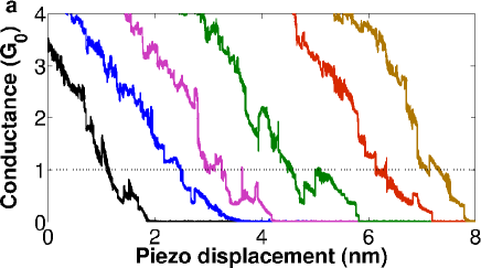
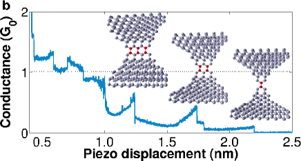
Cleavage techniques are becoming common in the quest for 2D crystalsRadisavljevi11 . With a few exceptionsHong10 , they remain largely unexplored in the field of topological insulators (TI’s). We report here, using scanning tunneling microscope (STM) based mechanical and electrical characterization techniques, the first evidence of the QSH phase in a two-dimensional crystal such as an exfoliated Bi(111) bilayer. The procedure follows closely that of creation of atomic size metallic contactsAgrait:physrep:03 , namely, repeated indentations of a tip against a surface while measuring the current at low voltages (typically 100 meV). The resulting conductance traces contain information on the atomic and electronic structure of the contact. The experiments where done at room temperature (and ambient conditions) and at low temperatures (4K) in cryogenic vacuum using two Bi samples of different originsupplementary . Related experiments have been reported in the pastKrans and van Ruitenbeek (1994); PhysRevLett.88.246801 ; PhysRevLett.78.4990 , lacking a convincing interpretation of the results, but have, in part, motivated our work.
As a rule of thumb (in particular for monovalent elements) each atom forming the minimum cross section of a metallic nanocontact contributes to the conductance with a value in the vicinity of Agrait:physrep:03 . Thus, on retracing the tip after indentation, one-atom cross-section contacts formed right before complete break-up are signaled by a conductance plateau (as a function of the STM piezo elongation) near the quantum of conductance . Unlike their more common metallic counterparts, the conductance traces of Bi nanocontacts at 4 K present several sub-plateaus below before break-up (see Fig. 1a). In Fig. 1b, we have singled out one trace that manifestly shows four sub-plateaus before the final rupture. Since each plateau corresponds to an elastic deformation of an atomic configuration in between plastic deformation events, one can only conclude that few-atom cross section Bi nanocontacts (as the ones shown in the insets) are much less conducting than their metallic counterparts. Being a common practice to record conductance histograms to statistically characterize nanocontactsAgrait:physrep:03 , we have done so using thousands of rupture traces. We find a large statistical weight below , but no characteristic values can be appreciatedsupplementary .
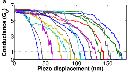
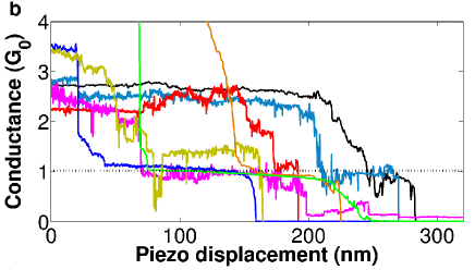
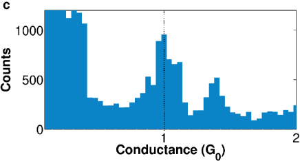
In air at 300 K the mechanical stability of the experimental set-up is inferior to that at low temperatures, making it more difficult to carry out measurements in a systematic way. Previously, the samples were fully characterizedsupplementary , paying attention to surface contamination and, in particular, to oxidation. This turned out to be very small, as long known for BiTahboub et al. (1979). Starting from conductance values at a maximum indentation of the order of 10, most of the traces either do not break for the allowed range of the piezo, typically up to 300 nm, or fall to zero showing no apparent reproducible behavior. Starting from smaller indentations (up to 3-6 ), however, consecutive traces may repeatedly show small features or short plateaus, including plateaus at (see Fig. 2a) which were completely absent in the 4 K measurements. Notice also the different length scales in Figs. 1a and 1b (1 nm) and Figs. 2a and 2b (100 nm). Most notably, long conductance plateaus appear on occasions on some traces (see Fig. 2b), the length of these reaching up to hundreds of nanometers. While some of them correspond to the initial elongation elastic process (the ones around ), most of them appear after a few plastic events. One way to quantify the information in these traces is to plot a conductance histogram only with them (we have selected those exhibiting plateaus longer that 50 nm regardless of the plateaus conductance values). The result is incontrovertible, showing a large peak at since most of the plateaus are largely pinned at the quantum of conductance (see Fig. 2c).
An exact conductance value of is generally expected to occur when, first, the Fermi wavelength is comparable to the constriction width and, second, the constriction potential is adiabatic in the current direction. This happens, for instance, in a gated two-dimensional electron gasvan Wees et al. (1991) or in monovalent metal atomic contactsAgrait:physrep:03 . Crystalline bulk Bi presents two types of carriers (electrons and holes) with long Fermi wavelengths (tens of nm) and unusually small massesPhysRevB.52.1566 . A first scenario, already put forward to explain the early experiments in Ref. PhysRevLett.88.246801, , invokes the formation of large cross section three dimensional constrictions (thousands of atoms) so that the lateral movement of the long-wavelength electrons gets quantized. It is, however, difficult to predict how the bulk electronic structure can carry over to constrictions presumably lacking long crystalline order. In addition, adiabaticity imposes severe restrictions to the shape of the constrictions. Furthermore, it is quite hard to imagine how these constrictions may be stable during very long piezo displacements. Even more difficult to accept is the fact that they must exist right before rupture without then going through a very large number of plastic deformation events. A second scenario where atom-size constrictions are responsible for the appearance of is ruled out by the observation of sub-quantum plateaus in most traces (see Figs. 1 and 2) and also by our calculations (see below).
We now give our rationale to our findings. Bulk Bi can be viewed as a layered material in the (111) directionsupplementary ; much as graphite, but with a stronger electronic coupling between layers. In fact, a Bi(111) bilayer is similar to graphene in many respects, in particular the atomic structure is that of a puckered honeycomb lattice, with the atoms of one sublattice shifted perpendicularly with respect to those of the other sublattice. A Bi(111) bilayer has been predicted to be a QSH insulatorPhysRevLett.97.236805 with a large bulk gap and three pairs of helical edge statesWada11 . This odd number of edge states guarantees that the transport properties of a Bi(111) flake should be robust against size, shape, and weak disorder. In particular, it should generically exhibit a universal two-terminal conductance of .
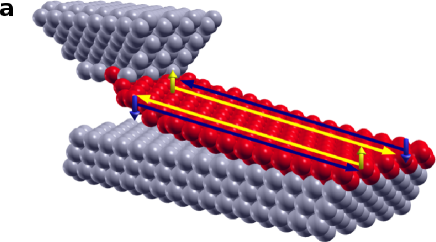
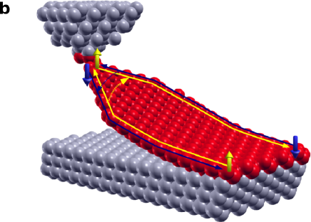
Given the layered structure of Bi, the general picture that naturally emerges from our experiments is that of a contact-induced exfoliation of a Bi(111) bilayer (see Figs. 3a and 3b). We first note that the inter-bilayer coupling is about ten times weaker than the intra-bilayer covalent bondingHofmann06 . The Bi(111) surface presents a Debye temperature in the 70-80 K rangeMayrhofer-Re12 so that at ambient conditions it should not come as a surprise that, once a gentle contact is made on the appropriate surface orientation, retracing the tip can peel off a single bilayer. One extreme of this bilayer (while the rest remains in contact with the surface) sticks to the tip which now acts as an electrode (see Figs. 3a, 3b and Supplemental Material moviesupplementary ). The specifics of the proposed mechanical exfoliation are unknown to us, being unclear whether the tip breaks the surface or simply elastically deforms it after indentation, and whether slip directions on the (111) planes favor slipping over detaching mechanisms. The number of atoms participating in the contact at maximum conductance is also unknown, but it remains large enough after exfoliation so that the theoretically expected intrinsic conductance of the bilayer is not masked by the contact resistance.
With this picture in mind, the conductance sub-plateaus below can only reflect the breaking of the tip-bilayer contact or the progressive breaking of the bilayer, a process in which a bidimensional nanocontact may form (see Fig. 3b and insets in Fig. 4a). Since a disordered Bi(111) bilayer is expected to exhibit a maximum conductance of , we can only expect the nanocontacts thus formed to conduct less due to inter-edge backscattering at the constriction (this is more clearly observed at 4 K). Noticeably, at 4 K, long plateaus do not appear near . We attribute this absence to the stronger inter-bilayer binding at low temperatures which prevents the exfoliation of a sufficiently large flake. Interestingly, the up-turns of the sub-plateaus rarely surpass .
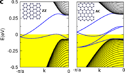
We now support our hypothesis with atomistic calculations. We model Bi with a 4-orbital tight-binding Hamiltonian with the parametrization given by Liu and AllenPhysRevB.52.1566 . In order to account properly for the electronic structure at the edges, we carry out self-consistent calculations including local electron-electron interactionssupplementary . As can be seen in Fig. 3c, Bi(111) bilayer nanoribbons grown along zigzag (ZZ) and armchair (AC) crystallographic orientations present a gap with valence and conduction bands connected in a continuous manner by an edge state band. This edge band cuts three times the Fermi energy and presents the same topology as that computed with more sophisticated DFT calculationsWada11 , which gives us confidence in our model. We have also verified that the nature of the wave functions in this band follows that expected in a QSH insulatorsupplementary .
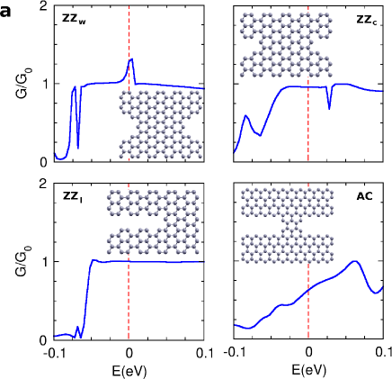
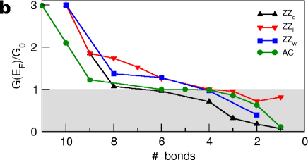
Equipped with a reliable atomistic description of Bi, we now perform coherent quantum transport calculations. (While inelastic effects cannot be entirely ruled out, bulk Bi carriers are known to have very long mean free paths even at room temperatureDas and Soundararajan (1987).) We introduce constrictions in the nanoribbons emulating the breaking of the bilayer flake (see insets in Fig. 4a). For simplicity’s sake we have chosen to perform this type of calculation instead of the one for a contact between a tip (of unknown shape) and the flake (as shown in Figs. 3a and 3b). A common way to calculate the conductance (as a function of energy) is through the Green’s function formalism and the partitioning techniqueALACANT ; Jacob11 ; supplementary , now taking fully into account the atomic SOCGosalbez-Mar11 ; supplementary . Results of for four different constriction geometries in AC and ZZ nanoribbons are shown in Fig. 4a. Figure 4b shows at the Fermi energy () for these four geometries as a function of the number of bonds at the constriction (i.e., as a function of the width). Only in disorder-free ribbons with perfectly defined edges the three channels can fully transmit. For constriction widths just two or three bonds smaller than that of the ribbons the conductance drops in all cases to values in the close vicinity of . Only constrictions featuring less than approximately five bonds conduct below . (The robust appearance of also holds for other types of disordersupplementary .) These results can be simply understood in terms of strong intra-edge backscattering of two of the edge channels and absent or partial inter-edge backscattering of the remaining helical pair at the narrowest section of the constriction (see Figs. 3a and 3b). Our estimate of a minimum of five bonds for a constriction to support is consistent with the maximum number of plastic events typically seen in the experiments below before the constriction definitely breaks (see, e.g., Fig. 1b).
In summary, we have reported and offered a consistent interpretation to the appearance of extremely long quantum of conductance plateaus in the breaking process of Bi nanocontacts. We attribute it to the occasional local exfoliation of Bi bilayers, predicted to be 2D topological insulators. Other interpretations cannot be ruled out, but should account for three extraordinary facts: (i) the quantum of conductance cannot be associated with a single-atom contact, but with a nanoscopic constriction, (ii) it appears at room temperature, and (iii) it is robust to small concentration of contaminants since the experiments are performed in air.
The first two authors, CS and DGM, contributed equally to this work. The former on the experimental side and the latter on the theoretical part. We thank the Spanish MICINN for financial support through Grant Nos. FIS2010-21883, FIS2011-23488, and CONSOLIDER CSD2007-0010 and Generalitat Valenciana through Grant Nos. ACCOMP/2012/127 and PROMETEO/2012/011. DG acknowledges the Centro de Computación Científica at UAM for computational support. Cristina Almansa is gratefully acknowledged for her help with the transmission electron microscope.
References
- (1) M. Z. Hasan and C. L. Kane, Rev. Mod. Phys. 82, 3045 (2010).
- (2) C. L. Kane and E. J. Mele, Phys. Rev. Lett. 95, 226801 (2005).
- (3) H. Zhang, C.-X. Liu, X.-L. Qi, X. Dai, Z. Fang, and S.-C. Zhang, Nature Physics 5, 438 (2009).
- (4) The Quantum Hall Effect, edited by R. E. Prange, S. M. Girvin, and K. v. Klitzing (Springer, 1986).
- (5) S. Murakami, Phys. Rev. Lett. 97, 236805 (2006).
- (6) M. König, S. Wiedmann, C. Brüne, A. Roth, H. Buhmann, L. W. Molenkamp, X.-L. Qi, and S.-C. Zhang, Science 318, 766 (2007).
- (7) C. Liu, T. L. Hughes, X.-L. Qi, K. Wang, and S.-C. Zhang, Phys. Rev. Lett. 100, 236601 (2008).
- (8) I. Knez, R.-R. Du, and G. Sullivan, Phys. Rev. Lett. 107, 136603 (2011).
- (9) P. Hofmann, Progress in Surface Science 81, 191 (2006).
- (10) Z. Zhang, D. Gekhtman, M. S. Dresselhaus, and J. Y. Ying, Chemistry of Materials 11, 1659 (1999).
- (11) F. Yang, L. Miao, Z. F. Wang, M.-Y. Yao, F. Zhu, Y. R. Song, M.-X. Wang, J.-P. Xu, A. V. Fedorov, Z. Sun, G. B. Zhang, C. Liu, F. Liu, D. Qian, C. L. Gao, and J.-F. Jia, Phys. Rev. Lett. 109, 016801 ( 2012).
- (12) C.-C. Liu, W. Feng, and Y. Yao, Phys. Rev. Lett. 107, 076802 (2011).
- (13) B. Radisavljevic, A. Radenovic, J. Brivio, V. Giacometti, and A. Kis, Nat. Nanotechnology 6, 147 (2011).
- (14) S. S. Hong, W. Kundhikanjana, J. J. Cha, K. Lai, D. Kong, S. Meister, M. A. Kelly, Z.-X. Shen, and Y. Cui, Nano Lett. 10, 3118 (2010).
- (15) N. Agraït, A. L. Yegati, and J. M. van Ruitenbeek, Physics Reports 377, 81 (2003).
- (16) Supplemental Material can be obtained upon request: juanjose.palacios@uam.es
- Krans and van Ruitenbeek (1994) J. M. Krans and J. M. van Ruitenbeek, Physical Review B 50, 17659 (1994).
- (18) J. G. Rodrigo, A. García-Martín, J. J. Sáenz, and S. Vieira, Phys. Rev. Lett. 88, 246801 (2002).
- (19) J. L. Costa-Krämer, N. García, and H. Olin, Phys. Rev. Lett. 78, 4990 (1997).
- Tahboub et al. (1979) R. M. Tahboub, M. E. Guindy, and H. D. Merchant, Oxidation of Metals 13, 545 (1979).
- van Wees et al. (1991) B. J. van Wees, L. P. Kouwenhoven, E. M. M. Willems, C. J. P. M. Harmans, J. E. Mooij, H. van Houten, C. W. J. Beenakker, J. G. Williamson, and C. T. Foxon, Physical Review B 43, 12431 (1991).
- (22) Y. Liu and R. E. Allen, Phys. Rev. B 52, 1566 (1995).
- (23) M. Wada, S. Murakami, F. Freimuth, and G. Bihlmayer, Physical Review B 83 121310, (2011).
- (24) M. Mayrhofer-Reinhartshuber, A. Tamtögl, P. Kraus, K. H. Rieder, and W. E. Ernst, J Phys Condens Matter 24, 104008 (2012).
- Das and Soundararajan (1987) V. D. Das and N. Soundararajan, Physical Review B 35, 5990 (1987).
- (26) J. J. Palacios, D. Jacob, M. Soriano, A. J. Pérez-Jiménez, E. S. Fabián, E. Louis, and J. A. Vergés, “ALACANT quantum transport package”, http://alacant.dfa.ua.es.
- (27) D. Jacob and J. J. Palacios, J. Chem. Phys. 134, 044118 (2011).
- (28) D. Gosálbez-Martínez, J. J. Palacios, and J. Fernández-Rossier, Physical Review B 83, 115436 (2011).