Donostia International Physics Center (DIPC), Paseo Manuel de Lardizabal 4, 20018 San Sebastián, Spain.
⋆22email: swxayfea@ehu.es
§22email: sqbsapod@ehu.es 33institutetext: †Present address: School of Engineering and Applied Sciences, Harvard University, Cambridge, Massachusetts 02138, USA.
33email: esantos@seas.harvard.edu.
First-Principles Study of the Electronic and Magnetic Properties of Defects in Carbon Nanostructures
Abstract
Understanding the magnetic properties of graphenic nanostructures is instrumental in future spintronics applications. These magnetic properties are known to depend crucially on the presence of defects. Here we review our recent theoretical studies using density functional calculations on two types of defects in carbon nanostructures: Substitutional doping with transition metals, and sp3-type defects created by covalent functionalization with organic and inorganic molecules. We focus on such defects because they can be used to create and control magnetism in graphene-based materials. Our main results are summarized as follows:
-
(i)
Substitutional metal impurities are fully understood using a model based on the hybridization between the states of the metal atom and the defect levels associated with an unreconstructed D3h carbon vacancy. We identify three different regimes, associated with the occupation of distinct hybridization levels, which determine the magnetic properties obtained with this type of doping;
-
(ii)
A spin moment of 1.0 is always induced by chemical functionalization when a molecule chemisorbs on a graphene layer via a single C-C (or other weakly polar) covalent bond. The magnetic coupling between adsorbates shows a key dependence on the sublattice adsorption site. This effect is similar to that of H adsorption, however, with universal character;
-
(iii)
The spin moment of substitutional metal impurities can be controlled using strain. In particular, we show that although Ni substitutionals are non-magnetic in flat and unstrained graphene, the magnetism of these defects can be activated by applying either uniaxial strain or curvature to the graphene layer.
All these results provide key information about formation and control of defect-induced magnetism in graphene and related materials.
1 Introduction
The experimental discovery of graphene, a truly two-dimensional crystal, has led to the rapid development of a very active line of research. Graphene is not only a fundamental model to study other types of carbon materials, but exhibits many uncommon electronic properties governed by a Dirac-like wave equation (Novoselov et al. 2004 and 2005) Graphene, which exhibits ballistic electron transport on the submicrometre scale, is considered a key material for the next generation of carbon-based electronic devices (Geim et al 2007, Castro Neto et al. 2009). In particular, carbon-based materials are quite promising for spintronics and related applications due to their long spin relaxation and decoherence times owing to the spin-orbit interaction and the hyperfine interaction of the electron spins with the carbon nuclei, both negligible (Hueso et al. 2008, Trauzettel et al. 2007, Tombros et al. 2007, Yazyev 2008). In addition, the possibility to control the magnetism of edge states in nanoribbons and nanotubes by applying external electric fields introduces an additional degree of freedom to control the spin transport (Son et al. 2006, Mañanes et al. 2008). Nevertheless, for the design of realistic devices, the effect of defects and impurities has to be taken into account. Indeed, a substantial amount of work has been devoted to the study of defects and different types of impurities in these materials. The magnetic properties of point defects, like vacancies, adatoms or substitutionals, have been recognized by many authors (Lehtinen et al. 2003, Palacios et al. 2008, Kumazaki et al. 2008, Santos et al. 2010a, Santos et al. 2010b, Fuhrer et al. 2010, Ugeda et al. 2010, Yazyev et al. 2007). It has now become clear that the presence of defects can affect the operation of graphene based devices and can be used to tune their response.
In the present Chapter, we provide a review of some recent computational studies on the role of some particular type of defects in determining the electronic and, in particular, the magnetic properties of graphene and carbon nanotubes (Santos et al. 2008, 2010a, 2010b, 2010c, 2011, 2012a, 2012b). We will consider two types of defects: Substitutional transition metals and covalently bonded adsorbates. For the substitutional transition metals, we first present some of the existing experimental evidence about the presence of such impurities in graphene and carbon nanotubes. Then, we summarize our results for the structural, electronic and magnetic properties of substitutional transition metal impurities in graphene. We show that all these properties can be explained using a simple model based on hybridization between the shell of the metal atoms and the defects states of an unrelaxed carbon vacancy. We also show that it is possible to change the local spin moment of the substitutional impurities by applying mechanical deformations to the carbon layer. This effect is studied in detail in the case of Ni substitutionals. Although these impurities are non-magnetic at a zero strain, we demonstrate that it is possible to switch on the magnetism of Ni-doped graphene either by applying uniaxial strain or curvature to the carbon layer. Subsequently, we explore the magnetic properties induced by covalent functionalization of graphene and carbon nanotubes. We find that the magnetic properties in this case are universal, in the sense that they are largely independent of the particular adsorbate: As far the adsorbate is attached to the carbon layer through a single C-C covalent bond (or other weakly-polar covalent bond), there is always a spin moment of 1 associated with each adsorbate. We show that this result can be understood in terms of a simple model based on the so-called vacancy, i.e. one orbital removed from a -tight-binding description of graphene. This model captures the main features induced by the covalent functionalization and the physics behind. In particular, using this model we can easily predict the total spin moment of the system when there are several molecules attached to the carbon layer simultaneously. Finally, we have also studied in detail the magnetic couplings between Co substitutional impurities in graphene. Surprisingly, the Co substitutional impurity is also well described in terms of a simple -vacancy model.
2 Substitutional Transition Metal Impurities in Graphene
2.1 Experimental Evidences
Direct experimental evidence of the existence of substitutional impurities in graphene, in which a single metal atom substitutes one or several carbon atoms in the layer, has been recently provided by Gan and coworkers (Gan et al. 2008). Using high-resolution transmission electron microscopy (HRTEM), these authors could visualize individual Au and Pt atoms incorporated into a very thin graphitic layer probably consisting of one or two graphene layers. From the real-time evolution and temperature dependence of the dynamics, they obtained information about the diffusion of these atoms. Substantial diffusion barriers (2.5 eV) were observed for in-plane migration, which indicates the large stability of these defects and the presence of strong carbon-metal bonds. These observations indicate that the atoms occupy substitutional positions.
In another experiment using double-walled carbon nanotubes (DWCNT) (Rodriguez-Manzo et al. 2010), Fe atoms were trapped at vacancies likewise the previous observations for graphene layers. In these experiments, the electron beam was directed onto a predefined position and kept stationary for few seconds in order to create a lattice defect. Fe atoms had been previously deposited on the nanotube surface before the defect formation. After irradiation, a bright spot in the dark-field image was observed. A quantitative analysis of the intensity profile showed an increase of the scattered intensity at the irradiated position relative to the center of the pristine DWCNT. This demonstrates that at the defect position, on the top or bottom side of the DWCNT, a Fe atom was trapped.
Recent evidence was also reported for substitutional Ni impurities in single-walled carbon nanotubes (SWCNT) (Ushiro et al. 2006) and graphitic particles (Banhart et al. 2000). Ushiro and co-authors (Ushiro et al. 2006) showed that Ni substitutional defects were present in SWCNT samples synthesized using Ni-containing catalysts even after careful purification. According to their analysis of X-ray absorption data (XANES), the most likely configuration for these defects has a Ni atom replacing a carbon atom.
The presence of substitutional defects in the samples can have important implications for the interpretation of some experiments. For example, substitutional atoms of transition metals are expected to strongly influence the magnetic properties of graphenic nanostructures. Interestingly, transition metals like Fe, Ni or Co are among the most common catalysts used for the production of SWCNTs (Dresselhaus et al. 2001). Furthermore, the experiments by Banhart and coworkers (Rodriguez-Manzo et al. 2009) have demonstrated that it is possible to create individual vacancies at desired locations in carbon nanotubes using electron beams. This experiment, combined with the observed stability of substitutional impurities, opens a route to fabricate new devices incorporating substitutional impurities at predefined locations. These devices would allow for the experimental verification of the unusual magnetic interactions mediated by the graphenic carbon network that have been predicted recently (Brey et al. 2007, Kirwan et al. 2008, Santos et al. 2010a). This becomes particularly interesting in the light of the recent finding that the spin moment of that impurities could be easily tuned by applying uniaxial strain and/or mechanical deformations to the carbon layer (Santos et al. 2008, Huang et al. 2011, Santos et al. 2012a). In spite of this, the magnetic properties of substitutional transition-metal impurities in graphenic systems were not studied in detail until very recently. Few calculations have considered the effect of this kind of doping on the magnetic properties of the graphenic materials, and this will be the main topic of the following sections.
2.2 Structure and Binding
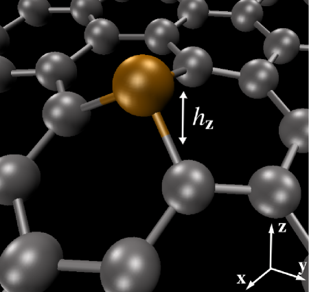
In Fig. 1 we show the typical geometry found in our calculations for a graphene layer where one carbon atom has been substituted by a metal impurity. The metal atom appears always displaced from the carbon layer. The height over the plane defined by its three nearest carbon neighbors is in the range 1.7-0.9 Å. These three carbon atoms are also displaced over the average position of the graphene layer by 0.3-0.5 Å. The total height (hz) of the metal atom over the graphene plane is the sum of these two contributions and ranges between 1.2-1.8 Å, as shown in panel (c) of Fig. 2.
In most cases the metal atom occupies an almost perfectly symmetric configuration with C3v symmetry. Exceptions are the studied noble metals, that are slightly displaced from the central position, and Zn that suffers a Jahn-Teller distortion in its most stable configuration. However, we have found that it is also possible to stabilize a symmetric configuration for Zn with a binding energy only 150 meV smaller. This configuration will be referred to as Zn throughout this chapter.
Figures 2(a)-(c) present a summary of the structural parameters of substitutional 3 transition metals, noble metals and Zn in graphene. Our calculations are in very good agreement with the results of a similar study performed by Krasheninnikov et al. (Krasheninnikov et al. 2009), although they overlooked the existence of the high-spin Zn configuration. Solid circles correspond to calculations using the Siesta code (Soler et al. 2002) with pseudopotentials (Troullier and Martins 1993) and a basis set of atomic orbitals (LCAO), while open squares stand for Vasp (Kresse and Hafner 1993, Kresse and Furthmüller 1996) calculations using plane-waves and PAW potentials (Blöchl 1994). As we can see, the agreement between both sets of calculations is excellent. Data in these figures correspond to calculations using a 44 supercell of graphene. For several metals we have also performed calculations using a larger 88 supercell and find almost identical results. This is particularly true for the total spin moments, which are less dependent on the size of the supercell, but require a sufficiently dense k-point sampling to converge. The behavior of the metal-carbon bond length and hz reflect approximately the size of the metal atom. For transition metals these distances decrease as we increase the atomic number, with a small discontinuity when going from Mn to Fe. The carbon-metal bond length reaches its minimum for Fe (dC-Fe=1.76 Å), keeping a very similar value for Co and Ni. For Cu and Zn the distances increase reflecting the fully occupied 3 shell and the large size of the 4 orbitals. Among the noble metals we find that, as expected, the bond length largely increases for Ag with respect to Cu, but slightly decreases when going from Ag to Au. The latter behavior is understood from the compression of the 6 shell due to scalar relativistic effects.
| dC-M(Å) | hz(Å) | (∘) | |
|---|---|---|---|
| Cu | 1.93, 1.90, 1.90 | 1.40 | 88.9, 88.9, 95.2 |
| Ag | 2.23, 2.19, 2.19 | 1.84 | 71.7, 71.7, 76.7 |
| Au | 2.09, 2.12, 2.12 | 1.71 | 78.0, 78.0, 81.6 |
| Zn | 2.06, 1.89, 1,89 | 1.54 | 88.3 88.3 103.9 |
| Zn | 1.99 | 1.67 | 87.9 |
As already mentioned, noble metals and Zn present a distorted configuration. In Table 1 we find the corresponding structural parameters. For Cu and Ag one of the metal-carbon bond lengths is slightly larger than the other two, whereas for Au one is shorter than the others. However, the distortions are rather small with variations of the bond lengths smaller than 2 %. The larger scalar relativistic effects in Au give rise to slightly smaller metal-carbon bond lengths for this metal as compared to Ag. In the case of Zn atoms, the distorted configuration presents one larger Zn-C bond (by 3.5%) and two shorter bonds (5%) compared with the bond length (1.99 Å) of the undistorted geometry. The distorted configuration is more stable by 160 meV (with SIESTA, this energy difference is reduced to 120 meV using VASP). This rather small energy difference between the two configurations might point to the appearance of non-adiabatic electronic effects at room temperature.
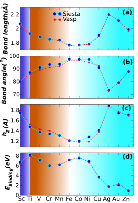
The binding energies of the studied substitutional metal atoms in graphene are shown in Fig. 2(d). In general, the binding energy correlates with the carbon-metal bond length, although the former exhibits a somewhat more complicated behavior. The binding energies for transition metals are in the range of 8-6 eV. Subtitutional Ti presents the maximum binding energy, which can be easily understood since for this element all the metal-carbon bonding states (Santos et al. 2010b) are fully occupied. One could expect a continuous decrease of the binding energy as we move away from Ti along the transition metal series, and the non-bonding 3 and the metal-carbon antibonding levels become progressively populated. However, the behavior is non-monotonic and the smaller binding energies among the 3 transition metals are found for Cr and Mn, and a local maximum is observed for Co. This complex behavior is explained by the simultaneous energy down-shift and compression of the 3 shell of the metal impurity as we increase the atomic number (Santos et al. 2010b). In summary, the binding energies of the substitutional 3 transition metals are determined by two competing effects: (i) as the 3 shell becomes occupied and moves to lower energies the hybridization with the carbon vacancy states near the Fermi energy (EF) is reduced, which decreases the binding energy; (ii) the transition from Mn to late transition metals is accompanied by a reduction of the metal-carbon bond length by 0.1 Å, which increases the carbon-metal interaction and, correspondingly, the binding energy.
The binding energies for noble metals are considerably smaller than for transition metals and mirror the reverse behavior of the bond lengths: 3.69, 1.76 and 2.07 eV, respectively, for Cu, Ag and Au. The smallest binding energy (1 eV) among the metals studied here is found for Zn, with both and electronic shells filled.
2.3 Spin Moment Formation: Hybridization between Carbon Vacancy and 3 Transition Metal Levels
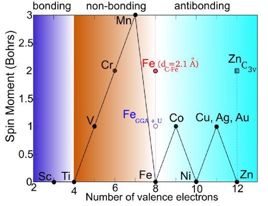
Our results for the spin moments of substitutional transition and noble metals in graphene are shown in Fig. 3 (Santos et al. 2010b). Similar results have been found by several authors (Krasheninnikov et al. 2009, Huang et al. 2011). We have developed a simple model that allows to understand the behavior of the spin moment, as well as the main features of the electronic structure, of these impurities (Santos et al. 2010b). Our model is based on the hybridization of the 3-states of the metal atom with the defect levels of a carbon vacancy in graphene. In brief, we can distinguish three different regimes according to the filling of electronic levels:
-
•
bonding regime: all the carbon-metal bonding levels are filled for Sc and Ti and, correspondingly, their spin-moments are zero;
-
•
non-bonding regime: non-bonding 3 levels become populated for V and Cr giving rise to a spin moment of, respectively, 1 and 2 with a strong localized character. For Mn one additional electron is added to the antibonding level and the spin moment increases to 3 ;
-
•
antibonding regime: finally, for Fe and heavier atoms all the non-bonding 3 levels are occupied and the spin moment oscillates between 0 and 1 as the antibonding metal-carbon levels become occupied.
The sudden decrease of the spin moment from 3 for Mn to 0 for Fe is characterized by a transition from a complete spin-polarization of the non-bonding 3 levels to a full occupation of those bands. However, this effect depends on the ratio between the effective electron-electron interaction within the 3 shell and the metal-carbon interaction (Santos et al. 2010b). If the hybridization with the neighboring atoms is artificially reduced, for example by increasing the Fe-C distance, Fe impurities develop a spin moment of 2 (see the red symbol in Fig. 3). Our results also show that it is possible to switch on the spin moment of Fe by changing the effective electron-electron interaction within the 3 shell. These calculations were performed using the so-called GGA+U method. For a large enough value of U (in the range 2-3 eV), Fe impurities develop a spin moment of 1 . It is noteworthy that this behavior is unique to Fe: using similar values of U for other impurities does not modify their spin moments.
| SM() | SC () | Stot () | |
| V | 1.21 | -0.09 | 1.0 |
| Cr | 2.53 | -0.20 | 2.0 |
| Mn | 2.91 | -0.10 | 3.0 |
| Co | 0.44 | 0.06 | 1.0 |
| Cu | 0.24 | -0.03, 0.31, 0.31 | 1.0 |
| Ag | 0.06 | -0.31, 0.54, 0.54 | 1.0 |
| Au | 0.16 | -0.28, 0.50, 0.50 | 1.0 |
| Zn | 0.23 | 0.37 | 2.0 |
At the level of the GGA calculations, Fe constitutes the border between two different trends of the spin moment associated with the substitutional metal impurities in graphene. For V, Cr and Mn the spin moment is mainly due to the polarization of the 3 shell of the transition metal atoms. The strongly localized character of the spin moment for those impurities, particularly for V and Cr, is corroborated by the Mulliken population analysis shown in Table 2. For Co, Ni, the noble metals and Zn the electronic levels close to the EF have a much stronger contribution from the carbon neighbors. Thus, for those impurities we can talk about a “defective graphene”-like magnetism. Indeed, it is possible to draw an analogy between the electronic structure of the late transition, noble metals and Zn substitutional impurities and that of the isolated unreconstructed (D3h) carbon vacancy (Santos et al. 2008, Santos et al. 2010a, Santos et al. 2010b). The stronger carbon contribution and delocalization in the distribution of the spin moment for Co, the noble metals and Zn impurities is evident in Table 2.
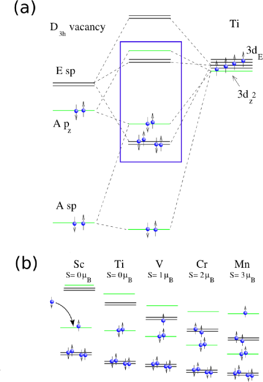
In the following we present the “hybridization” model that allows to distinguish the three regimes of the spin-moment evolution described before, corresponding to the filling of levels of different character. We have found that the electronic structure of the substitutional impurities can be easily understood as a result of the interaction of two entities: (i) the localized defect levels associated with a symmetric carbon vacancy and, (ii) the 3 states of the metal atom, taking also into account the down shift of the 3 shell as the atomic number increases. We considered explicitly the 3 states of the metal atom since our calculations show that, at least for transition metals, the main contribution from 4 orbitals appears well above EF.
To illustrate the main features of our model in Figure 4 (a) we present a schematic representation of the hybridization of the 3 levels of Ti with those of an unreconstructed carbon vacancy in graphene. The interested reader can see (Santos et al. 2010b) for an extension of the model for the other metals and technical details. The defect levels of the unreconstructed D3h vacancy can be easily classified according to their or character and whether they transform according to A or E-type representations. A scheme of the different level can be found in Fig. 4, while the results of a DFT calculation are depicted in Fig. 5 (b) (see also Santos et al 2010b and Amara et al 2007). Close to the EF we can find a fully symmetric A level (thus belonging to the A irreducible representation of the D3h point group) and two degenerated defect levels with E symmetry and character (E′ representation). Approximately 4 eV below EF we find another defect level with A character (A representation). Due to the symmetric position of the metal atom over the vacancy the system has a symmetry and the electronic levels of the substitutional defect can still be classified according to the or irreducible representations of this point group. Of course, metal and carbon vacancy states couple only when they belong to the same irreducible representation. Thus, occupied and vacancy levels can only hybridize with the 3 orbitals ( representation), while all the other 3 metal orbitals can only couple to the unoccupied vacancy levels.
With these simple rules in mind and taking into account the relative energy position of carbon and metal levels, that changes as we move along the transition metal series, we can understand the electronic structure of substitutional transition metals in graphene as represented in Fig. 4 (a) and (b). Some parameters in the model can be obtained from simple calculations. For example, a rough estimate of the position of the 3 shell of the metal atom respect to the graphene EF is obtained from the positions of the atomic levels. The relative strengths of the different carbon-metal hoppings can be estimated from those of the corresponding overlaps. With this information it is already possible to obtain most of the features of the model in Fig. 4. However, some uncertainties remain, particularly concerning the relative position of levels with different symmetry. To solve these uncertainties the simplest approach is to compare with first-principles calculations. The details of the model presented in Fig. 4 have been obtained from a thorough analysis of our calculated band structures (Santos at al. 2010b). In particular, we have used the projection of the electronic states into orbitals of different symmetry as an instrumental tool to classify the levels and to obtain the rational that finally guided us to the proposed model. In contrast, it is interesting to note that some features that derive from our way to understand the electronic structure of these defects are very robust and could actually be guessed without direct comparison with the calculated band structures. For example, the fact that for V we start to fill the non-bonding 3 states, and this impurity, as well as Cr and Mn, develops a spin moment, can be argued from simple symmetry and electron-counting arguments.
According to our model for the substitutional metals, there are three localized defect levels with character and three twofold-degenerate levels with character. Two of these levels correspond to bonding-antibonding - pairs, while the third one corresponds to 3 non-bonding states. For Sc-Mn the three levels can be pictured as a low lying bonding level with - character and a bonding-antibonding pair with - character. As shown in Fig. 4 we have four metal-vacancy bonding levels (two and one doubly-degenerate levels) that can host up to eight electrons. For instance, Ti contributes with four valence electrons, and there are four electrons associated with the localized carbon-vacancy levels. Ti has the bonding states completely occupied. Consequently, Ti presents the highest binding energy among all 3 transition metals and has a zero spin moment. Figure 4 (b) shows the situation for other impurities in the series Sc-Mn. Substitutional Sc impurities have zero spin-moment because they act as electron acceptors. Note that all the bonding levels are also filled for Sc, causing a p-doping of the graphene layer. As already mentioned V, Cr and Mn present an increasing spin moment due to the filling of the non-bonding levels, while for Fe the non-bonding shell is completely filled.
Late transition, noble metals and Zn substitutional impurities have the filled levels coming from an antibonding interaction between the carbon vacancy and the metal states. The character and spatial localization of those levels are very similar to those of the levels of the D3h vacancy close to EF.
Co substitutionals present a singly-degenerate half-occupied defect level at EF. As we will discuss in more detail in the next section, this level is reminiscent of the state that appears at EF associated with a single carbon vacancy in a -tight-binding description of graphene (Palacios et al. 2008). A second electron occupies this level for Ni impurities, and the spin polarization is lost (Santos et al. 2008).
An additional electron is added for noble metal impurities. This electron populates a doubly-degenerate level coming from the antibonding interaction of the 2 lobes in the nearest carbon neighbors, with the orbitals of dxz and dyz symmetries in the metal impurity. This state is reminiscent of E level of the D3h carbon vacancy. The occupation of this two-fold degenerate state with only one electron explains both, the observed 1 spin moment and the structural distortion of the noble metal impurities (Santos et al. 2010b). As we will see in Section 3.1, the E impurity levels also play a crucial role to explain the switching on of the magnetism of Ni impurities under mechanical deformations and uniaxial strain.
For Zn two electrons occupy the two-fold degenerate E level. As a consequence, the system suffers a Jahn-Teller distortion and has a zero spin moment. However, it is possible to stabilize a symmetric configuration (Zn) with a moment of 2 and only slightly higher in energy (Santos et al. 2010b).
2.4 Co Substitutionals in Graphene as a Realization of Single -vacancies
In this section we examine in detail the analogy that can be established between substitutional Co atoms in graphene (Cosub) and the simplest theoretical model trying to account for the properties of a carbon vacancy in graphene. The electronic structure and magnetic properties of a Cosub impurity are analogous to those of a vacancy in a simple -tight-binding description of graphene. This toy model system, the vacancy, has been extensively studied in the graphene literature due to its very interesting magnetic properties directly related to the bipartite character of the graphene network (Castro Neto et al. 2009, Palacios et al. 2008).
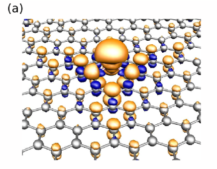
We begin by looking at the spin density of the Cosub impurity as shown in Figure 5 (a). The spin polarization induced in the carbon atoms has a -like shape and decays slowly as we move away from the impurity. The sign of the spin polarization follows the bipartite character of graphene: the polarization aligns parallel (antiparallel) to the spin moment located in the Co impurity for carbon atoms in the opposite (same) sublattice. The value of the total spin moment is 1.0 per defect. Using Mulliken population analysis, the moment on the Co atom has a value of 0.44 ; the three first carbon neighbors have 0.18 ; and there are 0.38 delocalized in the rest of the layer. Therefore, the total spin moment has contribution from both Co and carbon orbitals.
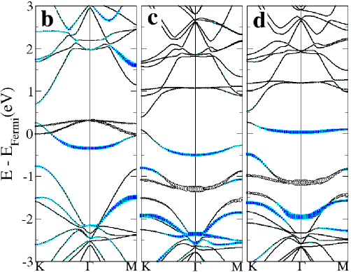
To understand the origin of this spin polarization, we now analyze in detail the band structure. Figures 5 (c) and (d) present the results for a Cosub defect in a 44 graphene supercell. Similar results are obtained using a 88 cell. For comparison, panel (b) shows the spin-compensated band structure of a single unreconstructed carbon vacancy. For the vacancy, there are three defect states in a range of 0.7 eV around EF. Two states appear above EF at 0.3 eV at and have a large contribution from the lobes of the C atoms surrounding the vacancy. These levels correspond to the two degenerate E states appearing in Figure 4. Another state at 0.35 eV below EF shows a predominant contribution and corresponds to the A level in Figure 4. This last level represents the defect state that appears at EF for a vacancy using a -tight-binding description. For a Cosub, the defect states of the vacancy described above hybridize with the Co states. The two defect bands, now an antibonding combination of Co and the original C vacancy levels, are pushed at higher energies, 1.0 eV above EF (see Fig. 5 (c) and (d)). The singly occupied state, now hybridized mainly with the Co orbital, remains at EF and becomes almost fully spin-polarized. The Cosub impurity becomes thus analogous to a vacancy in the -tight binding model of graphene.
This analogy is a powerful one, since it brings our results for the magnetism of Cosub impurities into contact with Lieb’s theorem for a half-filled Hubbard model (Lieb 1989), where the spin polarization is an intrinsic property of the defective bipartite lattice. Applying this theorem and our analogy, we can expect that the total spin of an array of Cosub impurities can be described according to the simple rule S=, where and indicate the number of Co substitutions in A and B sublattices, respectively. In Section 4.1 we will show results from first-principles calculations that confirm this behavior. However, Lieb’s theorem is global, in the sense that it refers to the total spin moment of the system, and does not enter into the local description of the magnetic interactions. This will be described in more detail in Section 4.1, where we will compute the exchange couplings between Cosub defects.
Other realistic defects, besides Cosub impurities, can also be mapped onto the simple -vacancy model. In Section 4.2 we will see that complex adsorbates chemisorbed on carbon nanotubes and graphene generate a spin polarization. The magnetism due to such a covalent functionalization displays a behavior similar to that of the -vacancies. Some concepts already used here will be again invoked to explain the main features of the magnetism associated with these defects, leading to a universal magnetic behavior independent of the particular adsorbate.
3 Tuning the Magnetism of Substitutional Metals in Graphene with Strain
In the previous section, we have considered in detail the formation of local spin-moments induced by a particular class of defects in graphene, substitutional transition metals. Although this is an important subject, other aspects are also crucial to understand and control the magnetism associated with this kind of doping. For example, one needs to explore the characteristics of the couplings between local moments, as well as the possibility to control such couplings, and the size of the local moments, using external parameters. This kind of knowledge is instrumental in possible applications in spintronics and quantum information devices. The subject of the magnetic couplings will be postponed until Section 4. In this Section we analyze how the structural, electronic and magnetic properties of substitutional defects in carbon nanostructures can be controlled using strain. We focus on Ni substitutionals and conclude that externally applied strain can provide a unique tool to tune the magnetism of Ni-doped graphene.
Strain provides a frequently used strategy to modify the properties of materials. For example, strain is intentionally applied to improve mobility in modern microelectronic devices. This so-called strain engineering has taken a key position over years. Recently, strain effects have also been proposed as a route to control the electronic properties of pristine graphene, which had a deep impact on the physics of this material (Guinea et al. 2009, Pereira et al. 2009).
Here, we show that the application of uniaxial strain can be used to switch on the magnetism of graphene doped with Ni substitutional impurities (Nisub) (Santos et al. 2012a). Whereas Nisub defects are non-magnetic in flat graphene, we find that their spin moment changes from zero when no strain in applied, up to 1.9 at 7.0% strain. This strong variation stems from the modifications of the local structure of the defect, which cause changes in the electronic structure of the defect that can be related to those of the unreconstructed carbon vacancy in graphene under strain. The similarities between the electronic structure of the D3h vacancy and that of Nisub were already stressed in the previous section.
We also show that substitutional metallic impurities in carbon nanotubes display a different magnetic behavior from that observed in flat graphene. Using Nisub dopants as an example we demonstrate that the intrinsic curvature of the carbon layer in the SWCNTs can be used to switch on the magnetism of Ni substitutionals (Santos et al. 2008). The defect electronic structure is modified by curvature in a similar way as by uniaxial strain. In addition, we find a strong dependence of the spin moment on the impurity distribution, tube metallicity and diameter of the nanotube.
3.1 Switching On the Magnetism of Ni-Doped Graphene with Uniaxial Strain
In this subsection, we study the electronic structure of Nisub defects in graphene under uniaxial strain. According to the analysis presented in Section 2.3, at a zero strain Nisub defects are non-magnetic in flat graphene (Santos et al. 2008, Santos et al. 2010b). However, we find that under moderate uniaxial strain these impurities develop a non-zero spin moment, whose size increases with that of the applied strain. This magnetoelastic effect might be utilized to design a strain-tunable spin device based on defective graphene.
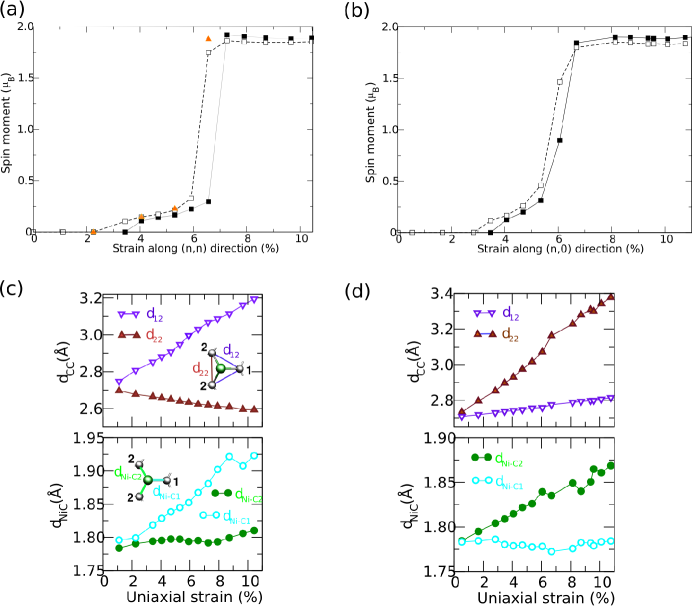
Figures 6 (a)-(b) show the spin moment of a Nisub defect as a function of the applied strain along the and directions, respectively. The curves with filled squares show simulations using geometries from a non-spin polarized calculation with a DZ basis set (see references Soler et al. 2002 and Artacho et al. 1999 for a description of the different basis sets). The spin moment and electronic structure are always calculated using a more complete DZP basis. The open squares indicate systems that were calculated using the previous procedure, i.e. a DZ basis, but the geometries have been obtained from spin-polarized calculations. The triangles display calculations with DZP basis set for both geometry and spin moment. At zero strain the Nisub defect is non-magnetic. As the uniaxial tension is applied, the system starts to deform. At 3.5% strain, the system becomes magnetic with a spin moment that evolves nearly linearly with the uniaxial strain up to values of at 6.0%. The magnetism of the system using different basis set is very similar. At 6.8% the spin moment increases sharply from 0.40 to 1.9 . This transition takes place for both directions, although it is somewhat more abrupt along the direction (Figure 6(a)) where no intermediate steps are observed. Thus, the magnetic properties depend on the local defect geometry and, to a much lesser extent, on the defect orientation relative to the applied strain. Panels (c) and (d) in Figure 6 present the local defect geometry. When the strain is applied, the triangle formed by the three C neighboring atoms to the Ni impurity deforms. The C-C distances along the strain direction increase, whereas distances along the perpendicular direction decrease in response to such elongation. The distance of the Ni atom to the first carbon neighbors also increases, but this bond length changes for the studied strains are less than 5.0% ( averaged over both strain directions) in comparison with 20.0% for the C-C distances. The analysis of distances suggests that the carbon neighbors and the central Ni impurity interact strongly, which is also reflected in the high stability of the defect with a binding energy 7.9 V to the carbon vacancy.
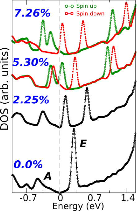
In order to understand the magnetic moment in Nisub defects, the density of states (DOS) around EF under strains of 0.0%, 2.2%, 5.3% and 7.2% are shown in Figure 7. The strain is along the direction although the qualitative behavior is similar to other directions. Several defect levels around EF have Ni and C mixed character. As pointed out before (Section 2), the metal atom over the vacancy has a symmetry at a zero strain, and the electronic levels are classified according to the or irreducible representations of this point group. Essentially, these three defect states and their evolution as a function of the applied strain determine all the observed physics.
One of them with character is occupied and appears around 0.50 eV below EF at a zero strain. This level comes from a fully symmetric linear combination of the orbitals (z-axis normal to the layer) of the nearest C neighbors interacting with the orbital of Ni. The other twofold-degenerate levels with character, coming from the hybridization of the in-plane lobes of the carbon neighbors with the Ni and orbitals, appear at 0.50 eV above EF at a zero strain. Because this electronic structure has the Ni states far from EF and no flat bands crossing EF, the spin moment of the Nisub impurity in graphene is zero. Interestingly, these three levels that appear close to EF in Figure 7 are reminiscent of those found for the unreconstructed carbon vacancy in graphene as we have already seen in Section 2.
The energy position of the three levels shifts as a function of the applied strain. When the strain is applied, the degeneracy between Ni C and Ni C states is removed and a gradual shift towards EF of one of them is observed. This level becomes partially populated, and the system starts to develop a spin moment. The Ni C state also changes its position approaching , although for small values of the strain this level does not contribute to the observed magnetization. However, around a 7% strain both the Ni C and the Ni C levels become fully polarized and the system develops a moment close to 2.00 .
Figure 7 also shows the resulting spin-polarized DOS at 5.3% and 7.2% strain (upper part of the panel). The exchange splittings of the and levels are, respectively, 0.29 eV and 0.13 eV at 5.3%, increasing with the applied strain and the associated spin moment. The energy gain with respect to the spin-compensated solutions develops from 13.9 meV at 5.3% to 184.1 meV at 7.26%. Thus, a moderate variation of the strain applied to the graphene layer changes the spin state and enhances the stability of the defect-induced moment. According to these results, if it is possible to control the strain applied to the graphene layer, as shown in recent experiments (Mohiuddin et al. 2009, Kim et al. 2009), the magnetism of Ni-doped graphene could be turned on and off at will, like switches used in magnetoelastic devices, however, with no applied magnetic field. This suggests a sensitive and effective way to control the magnetic properties of graphene, which is interesting for its possible applications in nanoscale devices (Santos et al. 2012a).
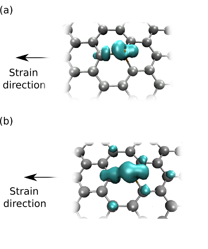
Figure 8(a)-(b) shows the spin magnetization patterns induced by the presence of a Nisub defect under two different magnitudes of uniaxial strain applied along the direction. The spin polarization induced in the neighboring carbon atoms has shape and orbital contributions that depend sensitively on strain. At 5.30% the spin density is mainly localized at the Ni impurity and at the C atom bonded to Ni along the strain direction. The anti-bonding character of the defect state that originates the magnetization is clear (see the node in the bond direction). The spin density at this C atom shows a -like shape to be contrasted with that at 7.26% strain, in which apart from the -like shape, a component is clearly observed. At this larger strain farther neighboring-carbon atoms also contribute to the spin density with mainly character. This additional contribution to the spin polarization pattern corresponds to the Ni C -defect state at EF for strains above 7%, as explained in the previous section using the DOS.
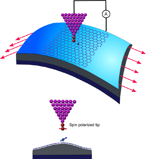
Figure 9 shows a possible experimental setup that could be used to test our predictions. This is similar to a mechanically controlled break junction setup with an elastic substrate (Mohiuddin et al. 2009, Kim et al. 2009). Graphene is deposited in the center of such a substrate in order to obtain a uniform strain. Bending or stretching the substrate causes an expansion of the surface, and the deposited graphene will follow this deformation. In principle, the modifications on the electronic structure can be detected using a scanning tunneling microscope (STM) since the defect levels that are involved are localized around the Fermi energy. For example, Ugeda et al. were able to measure using STM the energy position and spatial localization of the defect levels associated with a carbon vacancy in the surface of graphite (Ugeda et al. 2010). If the magnetic anisotropy of the defect is high enough, at sufficiently low temperatures, a preferential orientation of the moment would be stabilized and, in principle, a STM with a spin polarized tip (Spin-STM) could allow to monitor the evolution of the magnetic properties of the Ni-doped graphene with strain. Instead, an external magnetic field may be used to align the magnetic moments of the defects and define the hard/easy axis of the system. It is noteworthy that the break junction-like setup has already been successfully used (Standley et al. 2008).
3.2 Ni substitutionals in Carbon Nanotubes: Curvature Induced Magnetism
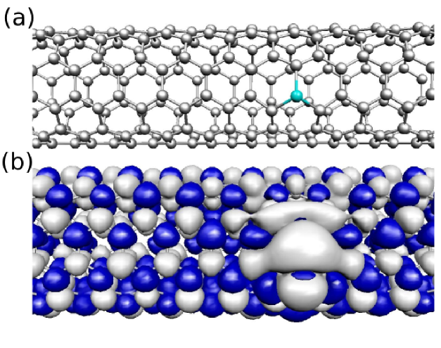
Although Nisub impurities are non-magnetic in flat graphene, their magnetic moment can be switched on by applying curvature to the structure. To understand why, we will begin looking at the equilibrium structure of Nisub for a (5,5) SWCNT. The Ni atom is displaced 0.9 Å from the carbon plane. Although both outward and inward displacements were stabilized, the outward configuration is more stable. The calculated Ni-C distances (dNi-C) are in the range 1.77-1.85 Å in good agreement with experiment (Ushiro et al. 2006, Banhart et al. 2000). Armchair tubes exhibit two slightly shorter and one larger values of dNi-C, the opposite happens for zigzag tubes, whereas for graphene we obtain a threefold symmetric structure with dNi-C=1.78 Å. Ni adsorption inhibits the reconstruction (Amara et al. 2007) of the carbon vacancy. Furthermore, we have checked that for a vacancy in graphene, a symmetric structure is obtained after Ni addition even when starting from a relaxed vacancy.
Figure 10 (b) shows the magnetization density profile for a Nisub defect in a (5,5) metallic nanotube at large dilution (0.3 % Ni concentration). The total spin moment is 0.5 . The magnetization is on the Ni atom and its C neighbors. However, it also extents considerably along the tube, particularly in the direction perpendicular to the tube axis. This profile indicates that the spin polarization follows some of the delocalized electronic states in the metallic nanotube. Indeed, as we clarify below, the magnetism in substitutionally Ni-doped SWCNTs only appears associated with the curvature and the metallicity of the host structure.
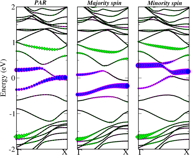
The basic picture described in Section 2 is still valid for the electronic structure of the Nisub impurity in SWCNTs. However, the modifications that appear due to the curvature of the carbon layer are responsible for the appearance of a magnetic moment. Figure 11 (a) shows the band structure of a paramagnetic calculation of a (5,5) SWCNT with a Nisub impurity every four unit cells. Comparing the band structure in Figure 11 (a) with the electronic structure of the Nisub impurity in flat geographer (lower curve in Figure 7), we appreciate the effects of curvature. The degeneracy between dxz and dyz states is removed (x-axis taken along the tube axis and y-axis along the tangential direction at the Ni site).
The dyz contribution is stabilized by several tenths of eV and a quite flat band with strong dyz character is found pinned at EF close to the Brillouin-zone boundary. Under these conditions, the spin-compensated solution becomes unstable and a magnetic moment of 0.48 is developed. Figures 11 (b) and (c) show, respectively, the band structure for majority and minority spins. The exchange splitting of the dyz level is 0.4 eV and the energy gain with respect to the paramagnetic solution is 32 meV.
In general, whenever a flat band with appreciable Ni 3 character becomes partially filled we can expect the appearance of a spin moment. The population of such an impurity level will take place at the expense of the simultaneous depopulation of some of the delocalized carbon levels within the host structure. For this reason, the development of a spin moment is more likely for Nisub impurities in metallic structures like the armchair tubes. The crucial role of the host states also explains the delocalized character of the magnetization density depicted in Fig. 10 (b). However, it is important to stress that the spin moment associated with a Nisub impurity in SWCNTs forms driven by the local curvature of the carbon layer, because the energy position of one of the impurity levels shifts downwards until it crosses EF. A schematic representation of this phenomenon is shown in Fig. 12 where we also emphasize the similarities between the levels of the Nisub defect and those of the unreconstructed carbon vacancy. Notice the similarities with the effects of uniaxial strain described in the previous Section. At large tube diameters, the limit of flat graphene with zero spin moment (see Section 2) is recovered.
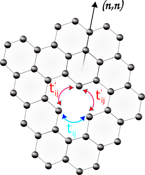
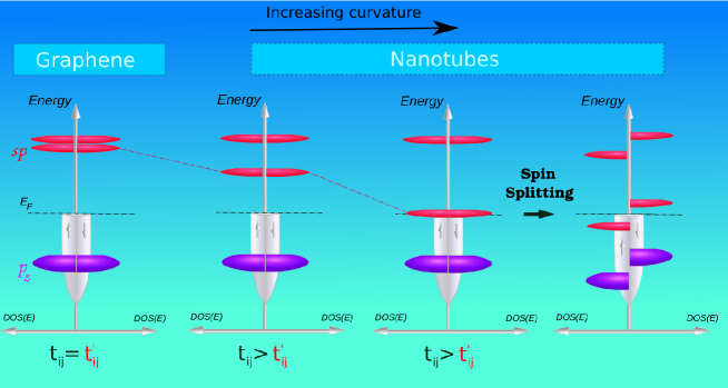
For semiconducting tubes, the situation is somewhat different. The and -like levels remain unoccupied unless their energies are shifted by a larger amount that pushes one of them below the top of the valence band. If the tube has a large enough gap, the spin moment is zero irrespective of the tube diameter. We have explicitly checked that a zero spin moment is obtained for (8,0) and (10,0) semiconducting tubes for Ni concentrations ranging from 1.5% to 0.5%. The different magnetic behavior of Nisub impurities depending on the metallic and semiconducting character of the host structure provides a route to experimentally identify metallic armchair tubes.
4 Magnetic Coupling Between Impurities
In previous Sections, we have considered the formation of local moments associated with defects in carbon nanostructures, as well as the use of mechanical deformations to tune the sizes of such local moments. Here, we present calculations of the exchange couplings between the local moments in neighboring defects. This is a necessary step to elucidate whether it is possible to induce magnetic order in these materials, which is crucial in the application of carbon-based nanostructures in spintronics. We focus on defects that can be mapped onto the simple model provided by the fictitious -vacancy. According to the results presented in Section 2.4, Co substitutional impurities belong to this class of defects. In this Section we present another type of impurities that behave according to the same analogy: molecules attached to graphene and carbon nanotubes through weakly-polar covalent bonds.
A -vacancy corresponds to a missing orbital in a graphene plane described using a -tight-binding model. The magnetic properties of the -vacancies have been extensively studied (Castro Neto et al. 2009, Palacios et al. 2008). Among other interesting properties, the magnetism of the -vacancy model reflects faithfully the bipartite character of the graphene lattice. For example, the total spin of the system is S=, where and are the number of -vacancies in each of the graphene sublattices. This behavior can be traced back to Lieb’s theorem for a half-filled Hubbard model in a bipartite lattice (Lieb 1989). In the following, we will see that the calculated data for Co substitutionals and covalently chemisorbed molecules indeed follow the predictions of Lieb’s theorem. In addition, we analyze in detail the spatial decay of the exchange couplings.
4.1 Magnetic Couplings Between Co Substitutional Impurities in Graphene
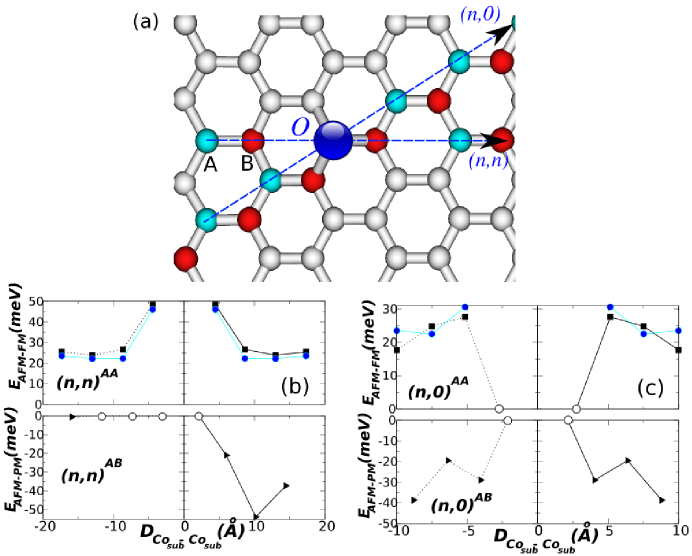
Here, we consider the magnetic couplings between Cosub defects. For this purpose we perform calculations using a large 88 supercell with two Cosub impurities. We calculate the energy difference between spin alignments as a function of the relative position of the defects. Figure 13 shows the results along with a schematic representation of our notation. Positive values indicate ferromagnetic (FM) spin alignment while negative values are antiferromagnetic (AFM) ones. Several observations from spin couplings in Fig. 13 can be made: (i) when the impurities are located in the same sublattice (AA systems) the FM configuration is more stable than the AFM one; (ii) if the Co atoms are in opposite sublattices (AB systems) it is very difficult to reach a FM solution, 111When we could stabilize a FM solution, it lies at higher energy, around 0.2 eV above the PAR one. instead the system finds either a spin-compensated (PAR) or an AFM solution; (iii) at short distances ( 3.0 Å) the systems always converge to spin compensated solutions.
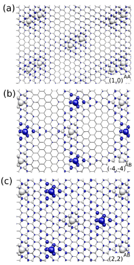
The FM cases of Fig. 13 always have total spin magnetization about 2.00 . The spin population on every Co atom remains almost constant 0.50 and it is 0.30 on the three C nearest-neighbors. In other cases the total spin is zero. Thus, the total spin moment of the system follows the equation , where N is the number of Cosub defects in the A(B) sublattices. Our total moment is consistent with Lieb’s theorem for bipartite lattices (Lieb 1989). This finding supports the analogy, presented in Section 2.4, between the electronic structure of Cosub defects and single vacancies in a simplified -tight-binding description of graphene.
Some selected configurations have their spin magnetization densities plotted in Fig. 14. Although the spin is quite localized on the Co atom and the neighboring C atoms, part of the magnetization density is delocalized with alternated signs in both graphene sublattices. The triangular spin patterns reflect the three-fold symmetry of the layer with different orientations for A and B substitutions. This explains the anisotropic AB interaction along the direction seen in Fig. 13 (b): the energy difference between AFM and PAR solutions for configurations strongly depends on the relative position of the impurities, showing such a directionality. Similar patterns have already been observed experimentally (Kelly et al. 1998, Mizes et al. 1989, Rutter et al. 2007, Ruffieux et al. 2000) for point defects in graphene using STM techniques and theoretically discussed for -vacancies (Yazyev 2008, Palacios et al. 2008, Pereira et al. 2008). For Cosub, similar STM experiments should display the topology of the spin densities given in Fig. 14.
We can also investigate the magnetic interactions within the framework of a classical Heisenberg model:
| (1) |
where is the local moment for a Cosub impurity at site . The angular dependence of the exchange is taken from an analytical RKKY coupling as given in (Saremi 2007). We fit the exponent for the distance decay to our ab initio results. The exchange interaction for AA systems can be fitted with a distance dependence (see the full circles in Fig.13 (b) and (c)). This distance dependence is in reasonable agreement with the behavior obtained with analytical models for substitutional defects and voids (Saremi 2007, Vozmediano et al. 2005). In the case of AB systems a simple RKKY-like treatment fails to describe accurately the interactions, at least for the short distances between defects considered in our calculations.
We next explain how PAR solutions appear in Fig. 13. The PAR solutions are stable because defect states in neighboring impurities interact strongly for AB systems. This interaction opens an appreciable bonding-antibonding gap in the defect band. 222For the AB systems, we find bonding-antibonding gaps in the impurity bands ranging from 0.3 eV to 0.9 eV for the and the configuration, respectively. These values are similar to the 0.5 eV spin-splitting of the Cosub defect. In fact, all those AB systems with gaps larger than 0.4 eV converge to PAR solutions. For AA systems, however, the bipartite character of the graphene lattice makes the interaction between the defects much smaller. This explains why AA configurations show a local spin polarization. Even for AA configurations, when the impurities are very close, non-magnetic solutions are stabilized because a larger defect-defect interaction opens a large gap. It is interesting to point out that similar behaviors have been observed for vacancies described within a -tight-binding model (see Section 1.6.1) (Yazyev 2008, Kumazaki et al. 2007, Palacios et al. 2008).
4.2 Covalent Functionalization Induces Magnetism: Universal Properties
In this Section we show that, apart from playing an increasingly important role in technological applications, chemical functionalization can be also used to induce spin moments in carbon nanostructures. Here, we focus on SWCNT and demonstrate that, when a single C-C bond is established on the carbon surface by covalent functionalization, a spin moment is induced into the system. This moment has a universal value of 1.0 and is independent of the particular adsorbate. In our recent work (Santos et al. 2011) we showed that this effect occurs for a wide class of organic and inorganic molecules of different biological and chemical activity (e.g. alkanes, polymers, diazonium salts, aryl and alkyl radicals, nucleobases, amido and amino groups, acids). Furthermore, we have recently found that a similar universal behavior is obtained for covalent functionalization of graphene (Santos et al. 2012b). We have also found that, either for metallic and semiconducting SWCNTs or for graphene, only when neighboring adsorbates are located at the same sublattice a spin moment is developed. For metallic tubes and graphene the local moments align ferromagnetically, while for semiconducting tubes we have almost degenerate FM and AFM spin solutions (Santos et al. 2011, Santos et al. 2012b).
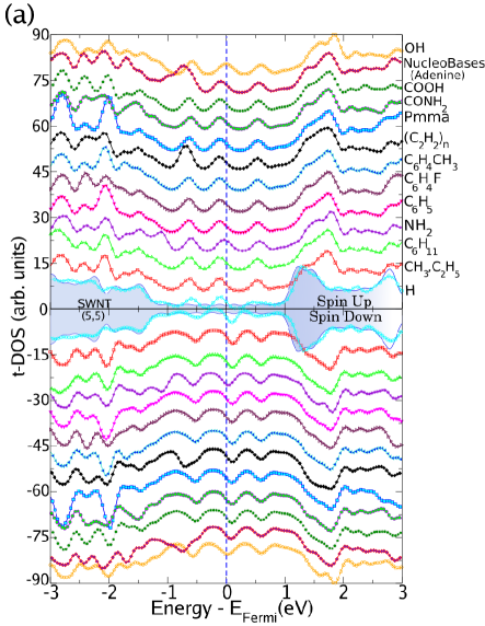
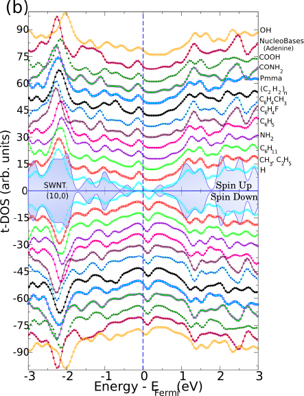
To understand the origin of the spin moment induced when a covalent bond is formed in the tube wall, we analyze the total spin-polarized density of states (t-DOS) when different adsorbates are attached to metallic and semiconducting tubes (see Figure 16 for the structure of some of these systems). Figure 15 presents results for (a) (5,5) and (b) (10,0) SWCNT’s. We consider first the well-known case of the adsorption of atomic hydrogen. In both cases, when a single H atom chemisorbs on top of a C atom a defect state appears pinned at EF with full spin polarization. This state is mainly composed of the orbitals at the nearest C neighbors of the defect site, with almost no contribution from the adsorbate. A detailed Mulliken analysis of this -defect state assigns a contribution of the adsorbate of about 1. Thus, the adsorbate has a primary role in creating the bond with the nanotube, and the associated defect level, but it does not appreciably contribute to the spin moment. More complex adsorbates, notwithstanding their biological and chemical activity (e.g. alkanes, polymers, diazonium salts, aryl and alkyl radicals, nucleobases, amido and amino groups, acids), show a similar behavior. This is observed in the t-DOS curves corresponding to other adsorbates in metallic (5,5) and semiconducting (10,0) SWCNTs as shown in Figure 15(a) and 15(b), respectively. Several common points are worth mentioning: (i) All molecules induce a spin moment of 1.0 localized at the carbon surface; (ii) The origin of the spin polarization corresponds to a -defect state with a character and a spatial distribution similar to those of the state appearing at EF for a -vacancy defect; (iii) The t-DOS around EF follows the same pattern in all cases. This match demonstrates that the spin moment induced by covalent functionalization is largely independent of the particular type of adsorbate. These results also demonstrate the complete analogy between a single C-H bond and more complex adsorbates linked to graphene through a single C-C bond (or other weakly-polar covalent bonds) (Santos et al. 2011, Santos et al. 2012b). Such similarity is not obvious and could not be easily anticipated.
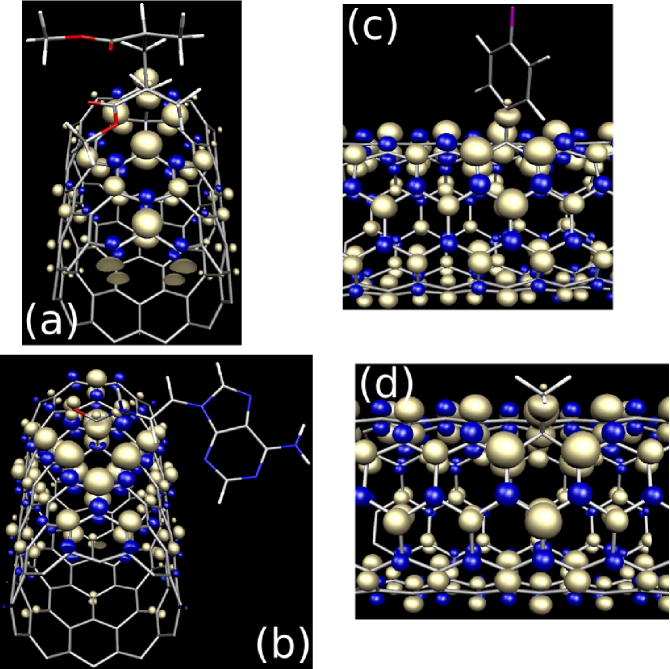
Next, we study the spin polarization texture induced by the adsorbates on the carbon nanotube wall. The analysis of local spin moments for all the adsorbates assigns general trends to both types, metallic and semiconducting, of SWCNTs. The C atoms that participate directly in the bond formation, at either the molecule or the surface, show a local spin moment smaller than . However, the wall carbon atoms contribute with 0.40 in the three first C nearest-neighbors, -0.10 in the next nearest-neighbors, 0.20 in the third-neighbors. The adsorbate removes a electron from the adsorption site, and leaves the states of the nearest carbon neighbors uncoordinated. This gives rise to a defect state localized in the carbon layer, reminiscent of that of a vacancy in a -tight-binding model of graphenic nanostructures. The carbon spins polarize parallel (antiparallel) respect to the C atom that binds to the surface when sitting in the opposite (same) sublattice. Figure 16 shows the magnetization density in semiconducting (10,0) and metallic (5,5) SWCNTs for several molecules: (a) Pmma polymer chain (Haggenmueller et al. 2000), (b) Adenine group nucleobase (Singh et al. 2009), (c) C6H4F salt (Bahr et al. 2001) and (d) CH3 molecule (Saini et al. 2002). The spin density in the metallic (5,5) (Figure 16(c) and 16(d)) is more spread over the whole surface than in the semiconducting (10,0) (Figure 16(a) and 16(b)). Thus, the electronic character of the nanotube wall plays a role in determining the localization of the defects states and, as will be seen below, in mediating the interaction between adsorbates.
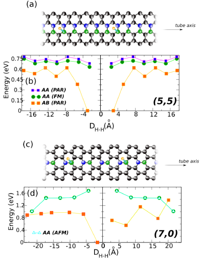
Now we deal with the relative stability of the different magnetic solutions when two molecules are simultaneously adsorbed on the walls of CNTs. Due to the universal character of the magnetism associated with covalent functionalization of SWCNTs, and in order to alleviate the computational effort, we have considered here hydrogen atoms. However, we have explicitly checked for some configurations for the case of SWCNTs, and for flat graphene (Santos et al. 2012b), that identical results are obtained when using CH3 instead of H. For the metallic (5,5) and semiconducting (7,0) single wall CNTs, we calculate the variation of the total energy for several spin alignments as a function of the distance between the adsorbates. The relative positions of the adatoms along the tube are schematically shown in Figures 17(a) and 17(c). One H is sited at the origin, and the other sites in different positions along of the tube axis. Several observations can be first made on the stability when two adsorbates are located at the same sublattice (AA configurations). In the metallic (5,5), the FM configuration is most stable than the non-magnetic one (PAR). The energy difference between these two spin solutions along the tube axis oscillates and no AFM solution could be stabilized at all. In the semiconducting (7,0), the FM and AFM solutions are almost degenerate, with a small energy difference (exchange coupling).
If the two molecules are now located at different sublattices (AB configurations), we were not able to stabilize any magnetic solution for both nanotubes. Instead the systems are more stable without magnetic polarization. This behavior for adsorbates at opposite sublattices is related to the interaction between the defect levels. As already pointed out for Co substitutionals, while for AA configurations the interaction is negligible, for AB ones this interaction opens a bonding-antibonding gap around in the defect band and, thus, contributes to the stabilization of PAR solutions. If the gap is larger than the spin splitting of the majority and minority spin defect bands the system will be non-magnetic (see Section 4.1). In fact, our detailed analysis of the band structure fully confirmed such an explanation. However, it is worth noting that AB adsorption seems to be always more stable in our calculations. This indicates that if the adsorption takes place at random sites, the magnetic solutions will only be stable for low density functionalization.
5 Conclusions
In this Chapter we have reviewed the structural, electronic and magnetic properties of two types of defects, substitutional metal impurities and -type covalent functionalization, in carbon nanostructures. We have focused on their role to induce and control magnetism in graphene and carbon nanotubes. Density functional theory was the main tool used to compute the properties of the studied systems. We also developed simple models to understand the observed trends. For instance, substitutional dopants in graphene were understood in terms of the hybridization of the states of the metal atoms with those of an unreconstructed carbon vacancy. The main ingredients of the model are the assumption of a three-fold symmetric bonding configuration and the approximate knowledge of the relative energy positions of the levels of the carbon monovacancy and the shell of the metal impurity as we move along the transition series. With this model, we understood the variations of the electronic structure, the size and localization of the spin moment, and the binding energy of transition, noble metals and Zn substitutional impurities in graphene (Santos et al 2010b). Our model also allowed us to draw an analogy between substitutionals of the late transition metals and the symmetric D3h carbon vacancy.
As a result of our analysis, a particularly powerful analogy was established between the substitutional Co impurity and the fictitious -vacancy in graphene (Santos et al 2010a). The -vacancy corresponds to a missing orbital in a simple description of graphene using a -tight-binding model. The magnetic properties of the -vacancies have been extensively studied. This analogy brings our results for the magnetism of Cosub defects into contact with the predictions of Lieb’s theorem for a half-filled Hubbard model in a bipartite lattice. We found that, according to Lieb’s theorem, the total spin of the system is S=, where and are the number of substitutions performed in each of the graphene sublattices. Thus, the couplings between local moments for AA substitutions are ferromagnetic and predominantly antiferromagnetic for AB substitutions. We have also used a simple RKKY-model to extract the distance decay of the couplings.
Adsorbates attached to graphene or SWCNTs through covalent bonds, particularly if the bonds are weakly polar, constitute another example of defects whose magnetism is analogous to that of the -vacancy. We have analyzed the magnetic properties induced by such a covalent functionalization using many types of adsorbates: polymers, diazonium salts, aryl and alkyl radicals, nucleobases, amide and amine groups, sugar, organic acids, for SWCNTs (Santos et al. 2011) and graphene (Santos et al. 2012b). A universal spin moment of 1.00 is induced on the carbon surface when a single C-C bond is formed between an adsorbate and the graphenic layer. In metallic carbon nanotubes and graphene, molecules chemisorbed at the same sublattice (AA adsorption) have their local moments aligned ferromagnetically. In semiconducting nanotubes, FM and AFM solutions are almost degenerate even for AA adsorption. For two molecules in different sublattices (AB adsorption), we could not stabilize any magnetic solution, and the system is more stable without a local spin moment.
We have also explored the possibility to control the magnetism induced by substitutional impurities using mechanical deformations. We have found that the spin moment of substitutionally Ni-doped graphene can be controlled by applying mechanical deformations that break the hexagonal symmetry of the layer, like curvature or uniaxial strain. Although Nisub impurities are non-magnetic in flat graphene, we have observed that stretching the layer by a few percents along different crystalline directions is enough to turn the non-magnetic ground state of Ni atoms embedded in graphene to a magnetic state (Santos et al. 2012a). The spin moment slowly increases as a function of the applied strain. However, at a critical strain value of 6.8%, a sharp transition to high spin (2 ) state is observed. This transition is independent of the orientation of the applied strain. A detailed analysis indicates that this strain-tunable spin moment is the result of changes of the positions of three defect levels around Fermi energy which are antibonding combinations of the Ni states and the and orbitals of the neighboring C atoms. This tunable magnetism observed in Nisub defects via strain control may play an interesting role in flexible spintronics devices.
Our calculations show that Nisub magnetism can also be switched on by applying curvature (Santos et al. 2008). For metallic carbon nanotubes the curvature of the carbon layer around the defect can drive the transition of the Nisub impurities to a magnetic state. For semiconducting tubes, the Nisub impurities remain non-magnetic irrespective of the tube diameter. We have analyzed in detail the origin and distribution of the magnetic moment. We found that the spin moment associated with Nisub impurities forms accompanied by the simultaneous polarization of delocalized electronic states in the carbon layer. Furthermore, the spin moment of Nisub is a signature of the metallicity of the structure: only metallic tubes develop a moment that depends on the tube diameter and Ni concentration.
Our work predicts a complex magnetic behavior for transition metals impurities in carbon nanotubes and graphene. This investigation is highly relevant in the interpretation of experimental results since it has been proposed that appreciable amounts of metal atoms could be incorporated into the carbon network, forming this type of substitutional defects in the course of synthesis, and are very difficult to eliminate afterwards. Our results also indicate that covalent functionalization provides a powerful route to tune the magnetism of graphene and carbon nanostructures. This is particularly attractive due to the recent successful synthesis of different graphene derivatives using surface chemical routes ( Cai et al. 2010, Treier et al. 2010). Thus, the synthesis of carbon nanostructures with functional groups at predefined positions, for example starting from previously functionalized monomers, seems plausible nowadays. According to our results, this could be applied to synthesize magnetic derivatives of graphene that behave according to well studied theoretical models like the -vacancy.
References
- (1) Amara, H., Latil, S., Meunier, V., Lambin, Ph., Charlier, J. C. (2007). Phys. Rev. B, 76: 115423.
- (2) Artacho, E., Sánchez-Portal, D., Ordejón, P., García, A., Soler, J. M. (1999) Phys. Status Solidi B, 215:809–817
- (3) Bahr, J. L., Yang, J., Kosynkin, D. V., Bronikowski, M. J., Smalley, R. E., Tour, J. M. (2001). J. Am. Chem. Soc., 123: 6536.
- (4) Banhart, F., Charlier, J. C., Ajayan, P. M. (2000). Phys. Rev. Lett., 84: 686.
- (5) Blöchl, P. E. (1994). Phys. Rev. B 50: 17953.
- (6) Brey, L., Fertig, H. A., Das Sarma, S. (2007). Phys. Rev. B, 99: 116802.
- (7) Cai, J., Ruffieux, P., Jaafar, R., Bieri, M., Braun, T., Blakenburg, S., Muoth, M., Seitsonen, A. P., Saleh, M., Feng, X., Müllen, K., Fasel, R., (2010) Nature, 466: 470.
- (8) Castro Neto, A. H., Guinea, F., Peres, N. M. R., Novoselov, K. S., Geim, A. K. (2009). Rev. Mod. Phys., 1: 109.
- (9) Chen, J. H., Li, L., Cullen, W. G., Williams, E. D., Fuhrer, M. S. (2010). Nat. Physics, 7:535.
- (10) Dresselhaus, M. S., Dresselhaus, G., Avouris, P. (2001). Carbon Nanotubes: Synthesis, Structure, Properties, and Applications , Springer Verlag.
- (11) Gan, Y., Sun, L., Banhart, F. (2008). Small, 4: 587.
- (12) Geim A. K., Novoselov, K. S. (2007). Nat. Materials, 6: 183.
- (13) Guinea, F., Katsnelson, M. I., Geim, A. K. (2010). Nature Physics, 6: 30.
- (14) Haggenmueller, R., Gommans, H. H., Rinzler, A. G., Fischer, J. E (2000). Chem. Phys. Lett., 330: 219.
- (15) Huang, B., Yu, J. J., Wei, S. H. (2011). Phys. Rev. B, 84: 075415.
- (16) Hueso, L. E., Pruneda, J. M., Ferrari, V., Burnell, G., Valdes-Herrera, J. P., Simons, B. D., Littlewood, P. B., Artacho, E., Fert, A., Mathur, N. D. (2008). Nature, 445: 410.
- (17) Kelly, K. F., Halas, N. J. (1998). Surface Science, 416: L1085.
- (18) Kim, K. S., Zhao, Y., Jang, H., Lee, S. Y., Kim, J. M., Kim, K. S., Ahn, J. H., Kim, P., Choi, J. Y., Hong, B. H. (2009). Nature, 457: 706.
- (19) Kirwan, D. F., Rocha, C. G., Costa, A. T., Ferreira, M. S. (2008). Phys. Rev. B, 77: 085432.
- (20) Krasheninnikov, A. V., Lehtinen, P. O., Foster, A. S., Pyykkö, P., Nieminen, R. M. (2009). Phys. Rev. Lett., 102: 126807.
- (21) Kresse, G., Hafner, J. (1993) Phys. Rev. B, 47:558
- (22) Kresse, G. Furthmüller J. (1996) Phys. Rev. B 54:11169
- (23) Kumazaki, H., Hirashima, D. S. (2008). Low Temperature Physics, 34: 805.
- (24) Kumazaki, H., Hirashima, D. S. (2007). Journal Phys. Soc. Jpn, 76: 064713.
- (25) Lehtinen, P. O., Foster, A. S., Ayuela, A., Krasheninnikov, A., Nordlund, K., Nieminen, R. M. (2003). Phys. Rev. Lett., 91: 017202.
- (26) Lieb, E. H. (1989). Phys. Rev. Lett., 62: 1201.
- (27) Mananes, A., Duque, F., Ayuela, A., Lopez, M. J., Alonso, J. A. (2008). Phys. Rev. B, 78: 035432.
- (28) Mizes, H. A., Foster, J. S. (1989). Science, 244: 559.
- (29) Mohiuddin, T. M. G., Lombardo, A., Nair, R. R., Bonetti, A., Savini, G., Jalil, R., Bonini, N., Basko, D. M., Galiotis, C., Marzari, N., Novoselov, K. S., Geim, A. K., Ferrari, A. C. (2009). Phys. Rev. B, 79: 205433.
- (30) Novoselov, K. S., Geim, A. K., Morozov, S. V., Jiang, D., Zhang, Y., Dubonos, S. V., Grigorieva, I. V., Firsov, A. A. (2004). Science, 306: 666.
- (31) Novoselov, K. S., Geim, A. K., Morozov, S. V., Jiang, D., Katsnelson, M. I., Grigorieva, I. V., Dubonos, S. V., Firsov, A. A. (2005). Nature, 438: 197.
- (32) Palacios, J. J., Fernandez-Rossier, J., Brey, L. (2008). Phys. Rev. B, 77: 195428.
- (33) Pereira, V. M., Lopes Santos, J. M. B., Castro Neto, A. H. (2008). Phys. Rev. B, 77: 115109.
- (34) Pereira, V. M., Castro Neto, A. H. (2009). Phys. Rev. Lett., 103: 046801.
- (35) Rodriguez-Manzo, J. A., Cretu, O., Banhart, F. (2010). ACS Nano, 4: 3422.
- (36) Rodriguez-Manzo, J. A., Banhart, F. (2009). Nano Letters, 9: 2285.
- (37) Ruffieux, P., Groning, O., Schwaller, P., Schlapbach, L., Groning, P. (2000). Phys. Rev. Lett., 84: 4910.
- (38) Rutter, G. M., Crain, J. N., Guisinger, N. P., Li, T., First, P. N., Stroscio, J. A. (2007). Science, 317: 219.
- (39) Saini, R. K., Chiang, I. W., Peng, H., Smalley, R. E., Billups, W. E., Hauge, R. H., Margrave, J. L. (2002). J. Am. Chem. Soc., 125: 3617.
- (40) Santos, E. J. G., Ayuela, A., Fagan, S. B., Filho, J. M., Azevedo, D. L., Filho, A. G. S., Sánchez-Portal, D. (2008). Phys. Rev. B, 78: 195420.
- (41) Santos, E. J. G., Sánchez-Portal, D., Ayuela, A. (2010a). Phys. Rev. B, 81: 125433.
- (42) Santos, E. J. G., Ayuela, A., Sánchez-Portal, D. (2010b). New Journal of Physics, 12: 053012.
- (43) Santos, E. J. G, Riikonen, S., Sánchez-Portal D., Ayuela, A. (2010c) arXiv:1012.3304
- (44) Santos, E. J. G., Sanchez-Portal, D., Ayuela, A. (2011). Appl. Phys. Lett., 99: 062503.
- (45) Santos, E. J. G., Ayuela, A., Sánchez-Portal, D. (2012a). J. Phys. Chem. C, 116: 1174.
- (46) Santos, E. J. G., Ayuela, A., Sánchez-Portal, D. (2012b) arXiv:1201.5326
- (47) Saremi, S. (2008). Phys. Rev. B, 76: 184430.
- (48) Singh, P., Kumar, J., Toma, F. M., Raya, J., Prato, M., Fabre, B., Verma, S., Bianco, A. (2009). J. Am. Chem. Soc., 131: 13555.
- (49) Soler, J.M., Artacho, E., Gale, J. D., García, A., Junquera, J., Ordejón, P., Sánchez-Portal, D. (2002). J. Phys.: Condensed Matter 14: 2745.
- (50) Son, Young-Woo, Cohen, M. L., Louie, S. G. (2006). Nature, 444: 347.
- (51) Standley, B., Bao, W., Zhang, H., Bruck, J., Lau, C. N., Bockrath, M. (2008). Nano Letters, 8: 3345.
- (52) Tombros, N., Jozsa, C., Popinciuc, M., Jonkman, H. T., van Wees, B. J. (2007). Nature, 448: 571.
- (53) Trauzettel, B., Bulaev, D. V., Loss, D., Burkard, G. (2007). Nature Physics, 3: 192.
- (54) Treier, M., Pignedoli, C. A., Laino, T., Rieger, R., Müllen, K., Passerone, D., Fasel, R., (2010). Nature Chemistry 3: 61.
- (55) Troullier, N., Martins J. L. (1991.) Phys. Rev. B 43: 1993.
- (56) Ugeda, M. M., Brihuega, I., Guinea, F., Gomez-Rodriguez, J. M. (2010). Phys. Rev. Lett., 104: 096804.
- (57) Ushiro, M., Uno, K., Fujikawa, T., Sato, Y., Tohji, K., Watari, F., Chun, W. J., Koike, Y., Asakura, K. (2006). Phys. Rev. B, 73: 144103.
- (58) Vozmediano, M. A. H., Lopez-Sancho, M. P., Stauber, T., Guinea, F. (2005). Phys. Rev. B, 72: 155121.
- (59) Yazyev, O. V. (2008). Nano Letters, 8: 1011.
- (60) Yazyev, O. V., Helm, L. H. (2007). Phys. Rev. B, 75: 125408.
- (61) Yazyev, O. V. (2008). Phys. Rev. Lett., 101: 037203.
- (62) Yazyev, O. V., Katsnelson, M. I. (2008). Phys. Rev. Lett., 100: 047209.