Theory of carrier density in multigated doped graphene sheets with quantum correction
Abstract
The quantum capacitance model is applied to obtain an exact solution for the space-resolved carrier density in a multigated doped graphene sheet at zero temperature, with quantum correction arising from the finite electron capacity of the graphene itself taken into account. The exact solution is demonstrated to be equivalent to the self-consistent Poisson-Dirac iteration method by showing an illustrative example, where multiple gates with irregular shapes and a nonuniform dopant concentration are considered. The solution therefore provides a fast and accurate way to compute spatially varying carrier density, on-site electric potential energy, as well as quantum capacitance for bulk graphene, allowing for any kind of gating geometry with any number of gates and any types of intrinsic doping.
pacs:
73.22.Pr, 41.20.Cv, 72.80.Vp, 85.30.DeIntroduction.
Manipulation of carrier density in graphene by electrical gating is one of the key techniques for graphene electronics. Since the first successful isolation of monolayer graphene flakes, conductance (resistance) sweep using a single backgate has been a standard electronic characterization tool for graphene.Novoselov et al. (2004) Double-gated graphene opens possibilities for experimental investigations of graphene pn and pnp junctions,Huard et al. (2007); Williams et al. (2007); Özyilmaz et al. (2007) which allow for exploration of the interesting physics of Klein paradox Klein (1929) in graphene.Katsnelson et al. (2006); Stander et al. (2009); Young and Kim (2009) In order to improve the junction quality, graphene heterojunctions using contactless top gates Liu et al. (2008); Gorbachev et al. (2008) and embedded local gates Nam et al. (2011); Lee et al. (2012) were proposed and investigated.
More complicated gating geometry is involved in recent proposals for graphene-based devices, such as a switching device with two topgates,Nakaharai et al. (2012) graphene transistors with self-aligned gates made by standard patterning with a regular cross section,Farmer et al. (2010) core-shell nanowires with round cross sections,Liao et al. (2010) or deposited films with T-shaped cross sections.Badmaev et al. (2012) Transport through bilayer graphene with multiple top gates up to eight was recently investigated;Miyazaki et al. (2012) patterning periodic top gates Weiss et al. (1989) on graphene to form quasi-one-dimensional superlattice is, in principle, feasible. Whereas a successful transport simulation relies decisively on the preciseness of the on-site potential profile, or equivalently the carrier density profile,Liu and Richter (2012) a more reliable theory to deal with general gating geometry is, therefore, imperative.
The theory of gate-induced carrier density started from the simplest classical capacitance model,Novoselov et al. (2004) which regards the graphene-substrate-backgate as a parallel-plate capacitor and the relevant carrier density in graphene as the surface charge density (divided by electron charge ) induced by the gate. Without taking into account the quantum correction due to the finite capacity of graphene itself for electrons to reside, this model can be straightforwardly generalized to arbitrary gating geometry by treating graphene as a perfect conducting plane with fixed zero potential. A more precise computation of the gate-induced carrier density, however, needs to take into account the relation between the induced charge density on graphene and the electric potential energy that those charge carriers gain, through the graphene density of states.Guo et al. (2007); Fernández-Rossier et al. (2007); Fang et al. (2007) The solution to the carrier density with such a correction taken into account requires a self-consistent iteration process Gorbachev et al. (2008); Shylau et al. (2009); Andrijauskas et al. (2012) that may be suitably termed the Poisson-Dirac method but actually corresponds to the quantum capacitance model,Luryi (1988) where an exact solution for single-gated pristine graphene at zero temperature has been derived.Fang et al. (2007)
In this paper, the spatial profile of carrier density in monolayer graphene due to arbitrary gating and doping is exactly solved within the quantum capacitance model. The solution has been further tested by comparing with the self-consistent Poisson-Dirac method, showing very good agreement between the two and, hence, their equivalence. A numerical example will be illustrated at the end. Throughout, we will restrict our discussion to bulk graphene at zero temperature and approximate the energy dispersion within the linear Dirac model, which leads to the density of states (per unit area) linear in energy, . The carrier density is given by integrating the density of states over the energy,
| (1) |
which is the underlying origin of the quantum correction to the gate-induced graphene carrier density in the following derivations. We are, therefore, working in the single-particle picture, and the solution within the quantum capacitance model to be presented is exact in the sense that no iteration is required during the solution process, as contrary to the following Poisson-Dirac method.
Self-consistent Poisson-Dirac iteration method.
Consider a graphene sheet laid in the - plain at . In the presence of a dopant concentration without electric gating, the quasi-Fermi level is given by
| (2) |
which is obtained from Eq. (1). When gate voltages of, in general, metalic gates are applied as sketched in Fig. 1, the electron in the graphene layer at gains an electrostatic potential energy , where is the electron charge and is the electrostatic potential at to be numerically solved from the Poisson equation
| (3) |
with the permittivity in free space and the relative permittivity that can be in principle position dependent.
The energy gain of the electron implies the raising of the energy band of graphene and, hence, the lowering of the quasi-Fermi level. The graphene carrier density therefore obeys Eq. (1) with
| (4) |
where is given by Eq. (2). Together with the charges of the dopant ions that maintain the neutrality of the graphene sheet, the net charge density on graphene divided by is given by
| (5) |
where is given by Eq. (4). Equation (5) is the boundary condition at the graphene sheet for the Poisson equation (3). This boundary condition contains the solution and, hence, makes the solution process iterative.
Quantum capacitance model.
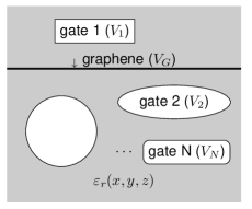
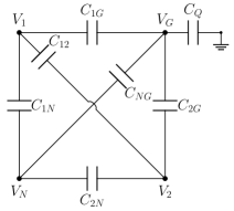
The system of metalic gates labeled by plus the graphene sheet labeled by as sketched in Fig. 1 is equivalent to the circuit plot shown in Fig. 1, where the quantum capacitance of the graphene sheet is considered. Regarding as the reference conductor with electric potential , the charge density on the surface of each gate can be expressed as
| (6) |
where are self-partial capacitances and with are mutual partial capacitances.Cheng (1989) Since the whole isolated system should remain charge neutral, the net charge density on should be the negative of the total charge density on the metalic gates: . The net electron number density on is, therefore, . Suppose there is an intrinsic doping concentration of in graphene. The net charge density on is not affected since the number of doped electrons should equal the number of dopant ions, . The net carrier density of graphene, however, is given by , which should obey Eq. (1), i.e., just like in the Poisson-Dirac method. We therefore need to solve the quadratic equation for ,
| (7) |
After some tedious but straightforward algebra, the carrier density of graphene in the presence of dopant concentration and gates with voltages is given by
| (8) |
where
| (9) |
is the classical contribution from doping and gating, and
| (10) |
arises solely from the quantum capacitance, leading to the second and third terms in Eq. (8) as the quantum correction. Equations (8)–(10) with and clearly recover the results for single-gated pristine graphene given in Ref. Fang et al., 2007. Contrary to the undoped case,Fang et al. (2007) the third term in Eq. (8) is responsible for the shift of the quasi-Fermi level due to doping and is typically weak for a reasonable .
In addition to the doping concentration that can have any kind of spatial profile, the position dependence enters the carrier density (8) through the self-partial capacitances , which can be computed numerically but exactly. For the th gate, by grounding all the other conductors including the graphene sheet, i.e., and , Eq. (6) suggests . The self-partial capacitance for gate is, therefore, given by
| (11) |
where can be numerically computed by any kind of finite-element simulator.
With the definitions (9) and (10), one may also write the solution to Eq. (7),
| (12) |
which has a reasonable form of charge divided by capacitance, with the numerator containing only the quantum correction terms in Eq. (8). The absence of in the numerator of agrees with our earlier remark that the classical capacitance model regards graphene as a perfect conducting plane with fixed zero potential so does not contribute to .
Equation (12) allows for a direct comparison with the iterative solution obtained from the self-consistent Poisson-Dirac method, as we will show with an explicit example soon. Multiplying Eq. (12) with the electron charge together with the quasi-Fermi level shift due to doping, provides for the graphene transport calculation a realistic on-site energy profile that guarantees a reliable quantum transport simulation; see, for example, Ref. Liu and Richter, 2012 for the case with neglected . Furthermore, the channel electrostatic potential given in Eq. (12) also allows us to write down the quantum capacitance of the graphene sheet in the low-temperature limit:Fang et al. (2007) .
Numerical example.
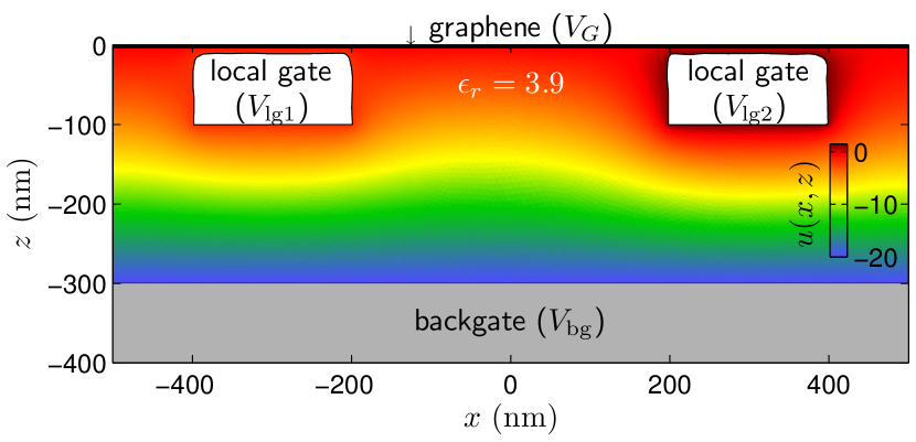
Armed with the above introduced theories, we next numerically demonstrate the equivalence of the quantum capacitance model to the self-consistent Poisson-Dirac iteration method by considering a specific example. To be simple but general, let us consider a quasi-one-dimensional system along with translation invariance along , composed of a doped graphene sheet gated by one flat backgate and two embedded local gates with irregular shapes roughly nm under graphene; see Fig. 2. Embedding such local gates at such a shallow depth allows independent control of the carrier density in the locally gated region due to screening of the backgate contribution and can be experimentally achieved; see, for example, Ref. Nam et al., 2011. The finite-element method is implemented in the iteration process for the Poisson-Dirac method as well as the exactly solvable self-partial capacitances [Eq. (11)] for the quantum capacitance model, and the pdetool in Matlab pde (2012) is chosen as the simulator for the present demonstration.
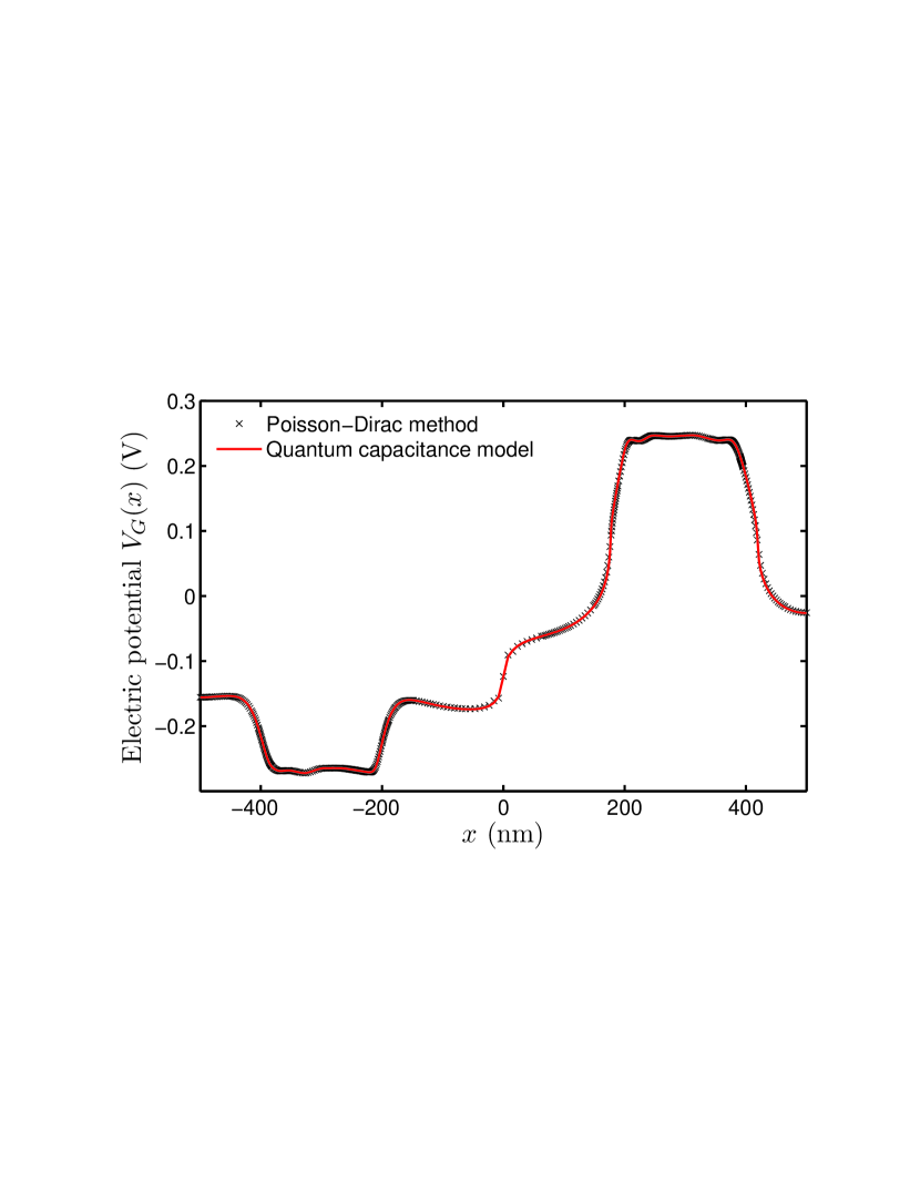
The electric potential shown in Fig. 2 is obtained by the self-consistent Poisson-Dirac method with backgate voltage and local gate voltages and and an intrinsic doping described by , where the position coordinate is in units of nm. The iterated potential solution at the graphene layer is compared in Fig. 2 with the exact solution (12) obtained within the quantum capacitance model, showing an excellent agreement with each other. With other gate voltages and other shapes of , the agreement remains exact. Note that the numerical example chosen here is basically a complicated version of Ref. Nam et al., 2011, including the proper range of the gate voltages, except that an artificial doping profile with hyperbolic tangent shape is considered, in order for the comparison to be general.
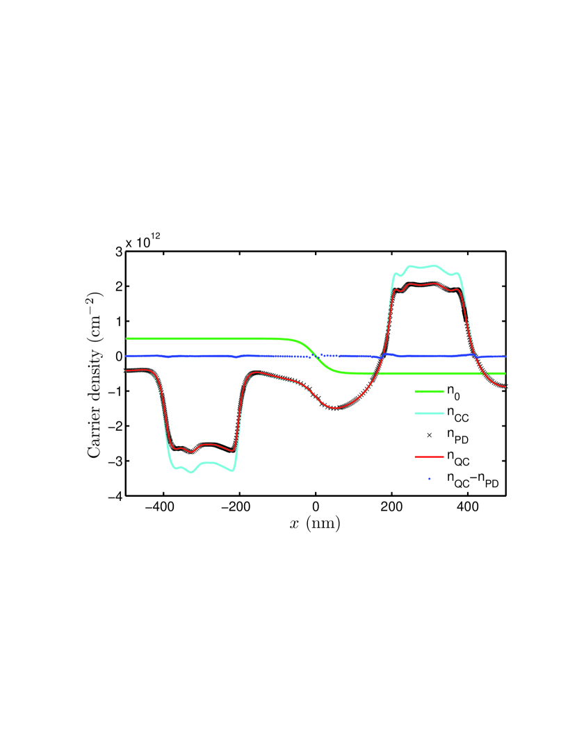
The spatial profiles of the carrier densities , , , , as well as the difference are shown in Fig. 3. Here the subscripts CC, PD, and QC denote “classical capacitance,” “Poisson-Dirac,” and “quantum capacitance,” respectively. The carrier density within the classical capacitance model is obtained by first computing the induced surface charge at with the graphene layer grounded () and then adding the dopant concentration or, equivalently, by Eq. (9) with the self-partial capacitances [Eq. (11)] numerically computed.
As the quantum correction, i.e., the second and third terms in Eq. (8), always reduces the magnitude of the net contribution of the gates, the classical solution always overestimates the gate-induced carrier density. This correction is especially salient when the gate is close to the graphene sheet, as is clearly observed by comparing or with in Fig. 3. In addition, the surface roughness of the embedded local gates considered here with such a short distance to the graphene sheet (roughly ) further introduces a strongly fluctuating potential profile [Fig. 2] as well as the corresponding carrier density profile (Fig. 3) at the locally gated regions.
As in the case of compared in Fig. 2, the agreement between and is rather satisfactory. In Fig. 3, the discrepancy between the Poisson-Dirac method and the quantum capacitance model becomes relatively obvious near positions where the surface charge density of the boundary condition (5) is changing its sign. This implies that the discrepancy may stem from the inherent numerical limitation of the chosen nonlinear partial differential equation solver.
Conclusion.
In conclusion, an exact solution for the space-resolved carrier density in multigated doped graphene sheets within the quantum capacitance model has been derived. With an illustrative quasi-one-dimensional example, the exact solution is shown to be equivalent to the self-consistent Poisson-Dirac iteration method. The solution therefore provides a fast and accurate way to compute spatially varying carrier density, on-site potential energy (key input for quantum transport simulation), as well as quantum capacitance for bulk graphene, allowing for any kind of gating geometry and any types of intrinsic doping. Moreover, the contact dopingGiovannetti et al. (2008); Khomyakov et al. (2009) and its corresponding screening potentialKhomyakov et al. (2010) can as well be treated by the presented solution, which therefore takes care of all three types of doping in graphene—electric, chemical, and contact-induced—in a unified manner.
Acknowledgments.
The author thanks K. Richter for valuable discussions and suggestions. Financial support by the Alexander von Humboldt foundation is gratefully acknowledged.
References
- Novoselov et al. (2004) K. S. Novoselov, A. K. Geim, S. V. Morozov, D. Jiang, Y. Zhang, S. V. Dubonos, I. V. Grigorieva, and A. A. Firsov, Science 306, 666 (2004).
- Huard et al. (2007) B. Huard, J. A. Sulpizio, N. Stander, K. Todd, B. Yang, and D. Goldhaber-Gordon, Phys. Rev. Lett. 98, 236803 (2007).
- Williams et al. (2007) J. R. Williams, L. DiCarlo, and C. M. Marcus, Science 317, 638 (2007).
- Özyilmaz et al. (2007) B. Özyilmaz, P. Jarillo-Herrero, D. Efetov, D. A. Abanin, L. S. Levitov, and P. Kim, Phys. Rev. Lett. 99, 166804 (2007).
- Klein (1929) O. Klein, Zeitschrift für Physik 53, 157 (1929).
- Katsnelson et al. (2006) M. I. Katsnelson, K. S. Novoselov, and A. K. Geim, Nat. Phys. 2, 620 (2006).
- Stander et al. (2009) N. Stander, B. Huard, and D. Goldhaber-Gordon, Phys. Rev. Lett. 102, 026807 (2009).
- Young and Kim (2009) A. F. Young and P. Kim, Nat. Phys. 5, 222 (2009).
- Liu et al. (2008) G. Liu, J. J. Velasco, W. Bao, and C. N. Lau, Appl. Phys. Lett. 92, 203103 (2008).
- Gorbachev et al. (2008) R. V. Gorbachev, A. S. Mayorov, A. K. Savchenko, D. W. Horsell, and F. Guinea, Nano Letters 8, 1995 (2008).
- Nam et al. (2011) S.-G. Nam, D.-K. Ki, J. W. Park, Y. Kim, J. S. Kim, and H.-J. Lee, Nanotechnology 22, 415203 (2011).
- Lee et al. (2012) J. Lee, L. Tao, Y. Hao, R. S. Ruoff, and D. Akinwande, Appl. Phys. Lett. 100, 152104 (2012).
- Nakaharai et al. (2012) S. Nakaharai, T. Iijima, S. Ogawa, H. Miyazaki, S. Li, K. Tsukagoshi, S. Sato, and N. Yokoyama, Applied Physics Express 5, 015101 (2012).
- Farmer et al. (2010) D. B. Farmer, Y.-M. Lin, and P. Avouris, Appl. Phys. Lett. 97, 013103 (2010).
- Liao et al. (2010) L. Liao, Y.-C. Lin, M. Bao, R. Cheng, J. Bai, Y. Liu, Y. Qu, K. L. Wang, Y. Huang, and X. Duan, Nature 467, 305 (2010).
- Badmaev et al. (2012) A. Badmaev, Y. Che, Z. Li, C. Wang, and C. Zhou, ACS Nano 6, 3371 (2012), http://pubs.acs.org/doi/pdf/10.1021/nn300393c .
- Miyazaki et al. (2012) H. Miyazaki, S.-L. Li, S. Nakaharai, and K. Tsukagoshi, Appl. Phys. Lett. 100, 163115 (2012).
- Weiss et al. (1989) D. Weiss, K. von Klitzing, K. Ploog, and G. Weimann, Europhysics Letters 8, 179 (1989).
- Liu and Richter (2012) M.-H. Liu and K. Richter, Phys. Rev. B 86, 115455 (2012).
- Guo et al. (2007) J. Guo, Y. Yoon, and Y. Ouyang, Nano Letters 7, 1935 (2007).
- Fernández-Rossier et al. (2007) J. Fernández-Rossier, J. J. Palacios, and L. Brey, Phys. Rev. B 75, 205441 (2007).
- Fang et al. (2007) T. Fang, A. Konar, H. Xing, and D. Jena, Appl. Phys. Lett. 91, 092109 (2007).
- Shylau et al. (2009) A. A. Shylau, J. W. Kłos, and I. V. Zozoulenko, Phys. Rev. B 80, 205402 (2009).
- Andrijauskas et al. (2012) T. Andrijauskas, A. A. Shylau, and I. V. Zozoulenko, Lithuanian Journal of Physics 52, 63 (2012).
- Luryi (1988) S. Luryi, Appl. Phys. Lett. 52, 501 (1988).
- Cheng (1989) D. K. Cheng, Field and Wave Electromagnetics, 2nd ed. (Prentice Hall, 1989).
- pde (2012) Partial Differential Equation ToolboxTM User’s Guide, The MathWorks, Inc., matlab 2012a ed. (2012).
- Giovannetti et al. (2008) G. Giovannetti, P. A. Khomyakov, G. Brocks, V. M. Karpan, J. van den Brink, and P. J. Kelly, Phys. Rev. Lett. 101, 026803 (2008).
- Khomyakov et al. (2009) P. A. Khomyakov, G. Giovannetti, P. C. Rusu, G. Brocks, J. van den Brink, and P. J. Kelly, Phys. Rev. B 79, 195425 (2009).
- Khomyakov et al. (2010) P. A. Khomyakov, A. A. Starikov, G. Brocks, and P. J. Kelly, Phys. Rev. B 82, 115437 (2010).