A generic tight-binding model for monolayer, bilayer and bulk MoS2
Abstract
Molybdenum disulfide (MoS2) is a layered semiconductor which has become very important recently as an emerging electronic device material. Being an intrinsic semiconductor the two-dimensional MoS2 has major advantages as the channel material in field-effect transistors. In this work we determine the electronic structure of MoS2 with the highly accurate screened hybrid functional within the density functional theory (DFT) including the spin-orbit coupling. Using the DFT electronic structures as target, we have developed a single generic tight-binding (TB) model that accurately produces the electronic structures for three different forms of MoS2 - bulk, bilayer and monolayer. Our TB model is based on the Slater-Koster method with non-orthogonal sp3d5 orbitals, nearest-neighbor interactions and spin-orbit coupling. The TB model is useful for atomistic modeling of quantum transport in MoS2 based electronic devices.
Molybdenum disulfide (MoS2) belongs to a family of layered transition metal dichalcogenides (TMDC) in which the layers are held together by weak van der Waals forces, and it can be exfoliated mechanically to a single layer thickness. In its bulk form MoS2 is an indirect band gap semiconductor which turns into a direct band gap semiconductor for monolayer structure.rHeinz This intrinsic semiconducting nature of MoS2 is a major advantage over graphene (which has no intrinsic band gap) as a two-dimensional (2D) channel material in field-effect transistors (FET). Indeed, FET devices based on MoS2 monolayer and bilayer have already been fabricated in the experimental labs and demonstrated to have useful device performances.rKis ; rLiu Several theoretical studies of MoS2 FET devices rSayeef ; rGuo ; rKalam based on simplified description of the electronic structures within an effective mass model have also been reported recently.
Due to the complex nature of the layered TMDC materials and the great interests in the electronics community for its applications in emerging devices, a more reliable, accurate, and atomistic treatment of the electronic structures of TMDC is desired. Since ab initio models are computationally expensive and often intractable for realistic device structures having large number of atoms, a widely applied intermediary option is the tight-binding (TB) model. TB models are atomistic full-band yet computationally efficient due to the small number of basis orbitals and the rigid nature of the Hamiltonian. Properly parameterized TB models have been extensively applied to predict reliable results for a diverse range of devices including the resonant tunneling diodes, rRoger quantum dots, rGerhard Si nanowireFET, rMathieu and compound semiconductor heterostructures.rIntel However, for the very exciting 2D MoS2 and other TMDC materials, accurate TB models for electronic structures has not yet been developed. It is the purpose of this work to fill this void, and the resulting TB model should be extremely useful for predicting quantum transport properties of MoS2 based devices.
In particular, we have developed a generic TB model with non-orthogonal sp3d5 orbitals including the nearest-neighbour interactions and spin-orbit coupling, that accurately determines the electronic structures of bulk, monolayer and bilayer MoS2. A reliable and accurate target band structure is the primary requirement for a successful tight-binding modeling. In this study, for the calculations of the target band structures we employ density functional theory (DFT) with the screened hybrid functional of Heyd, Scuseria, and Ernzerhof rHeyd1 (HSE) that has been shown in the literature rKresse1 ; rKresse2 ; rHyd2 to produce accurate band gaps and reasonable effective masses for a wide range of semiconductors. Our calculated band structures of MoS2 from the self-consistent DFT-HSE shows excellent agreement with the available experimental data and compare well with other theoretical studies.rLamb ; rEllis ; rWalle Even though an accurate target band structure is obtained by DFT-HSE, it is nontrivial to develop a generic TB model which can accurately capture electronic structures and effective masses of not only bulk MoS2 but also its double-layer and single-layer forms. For the layered TMDC structures there is a thickness dependent interlayer interaction that significantly affects the electronic properties, the TB model must capture these effects so as to be applicable to devices made of different layer thicknesses. As shown below, our generic TB model accurately produces the band structures for three different forms of MoS2: bulk, monolayer and bilayer. The reported TB model can be easily extended to other MoS2 structures of higher number of layers as well as other layered TMDC materials such as WS2, WSe2, and MoSe2. The accuracy of our TB model is validated by comparing the band gaps and effective masses with our calculated ab initio results.
In our study, all the DFT-HSE calculations are performed using the projector augmented-wave (PAW) pseudopotential plane-wave method as implemented in the VASP software package.rVasp A Monkhorst-Pack scheme is adopted for the sampling of the Brillouin zone with k-point meshes of for the bulk and for the two-dimensional (2D) structures. An energy cutoff of eV is used in a plane wave basis set. We also included the spin-orbit coupling self-consistently. Due to the presence of van der Waals interaction which determines the interlayer distance in MoS2, geometry optimization becomes quite tricky and complicated. Without the van der Waals intereaction the lattice parameter (vertical length of the unit cell) is overestimated by a large margin. However, it is not yet possible to include van der Waals interaction in the HSE calculations, and it is an area of active research. We therefore optimize the bulk crystal structure using the Perdew-Burke-Ernzerhof (PBE) functional rPBE for which the van der Waals interaction can be included explicitly by adopting the DFT-D2 method. rvdW We then use this optimized structure for the HSE calculations. The values of our optimized lattice parameters for bulk MoS2 are: Å and Å with a layer thickness of Å (S-S vertical distance). Although the value of parameter improves significantly with the DFT-D2 method, it is still overestimated by around compared to the experimental value.
It is a well-known fact that DFT within the local density approximation (LDA) or the generalized gradient approximation (GGA) underestimates band gaps of semiconductors due to factors such as the self interactions. This error can be minimized in the HSE scheme of hybrid functional methodrHeyd1 by incorporating short-range (SR) exact Hartree-Fock (HF) exchange with the PBE functional. A screening parameter defines the range separation, and is empirically set to Å-1 (HSE06 scheme) for both the HF and PBE parts. In our calculations for MoS2 we observe that the band gap energies vary significantly with the screening parameter for both the bulk and the D structures. We therefore decided to adjust the value of to fit the experimental band gap, and an optimize value for is found to be Å-1 which corresponds to an interaction range of Å for the SR nonlocal exchange. Note that a single value of is used for all the three structures of MoS2: bulk, double-layer and single-layer, namely the HSE results presented here were all obtained using Å-1.
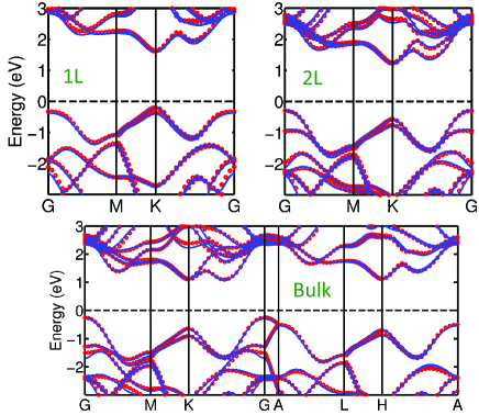
Our calculated band structure results for MoS2 are plotted in Fig. 1. We notice that the monolayer MoS2 has a direct band gap at the K point. However, with the addition of just one extra layer (i.e. for a bilayer structure) an indirect band gap opens up due to the presence of interlayer interactions. Although both bulk and bilayer MoS2 have indirect band gaps the conduction band minima (CBM) are located at different points: for bulk it is at point (midpoint of and K points) and for bilayer it is at K point. Similar behavior is observed in a previous theoretical study. rLamb For monolayer MoS2 the splitting of the valence band maximum (VBM) at K point is solely due to the spin-orbit coupling (SOC) whereas a combination of SOC and interlayer interactions is responsible for the VBM splitting in bulk and bilayer MoS2. The splitting of CBM due to SOC is minimal (around meV). The calculated band gap energies for different transitions are presented in Table 1. Our DFT-HSE results show good agreement with the experimental data. The values of effective masses at different band edges along different directions as presented in Table 2 also compare well with other available theoretical studies. rLamb ; rWalle
| Structure | Gap | HSE (target) | TB (fitted) | Deviation (%) | Exp. |
|---|---|---|---|---|---|
| Monolayer | Kv1 to Kc | 1.786 | 1.805 | 1.06 | 1.90 |
| Kv2 to Kc | 1.974 | 1.969 | 0.24 | 2.05 | |
| Bilayer | to Kc | 1.480 | 1.516 | 2.41 | 1.60 |
| Kv1 to Kc | 1.779 | 1.792 | 0.76 | 1.88 | |
| Kv2 to Kc | 1.980 | 1.987 | 0.35 | 2.05 | |
| Bulk | to | 1.328 | 1.331 | 0.22 | 1.29 |
| Kv1 to Kc | 1.776 | 1.749 | 1.46 | 1.88 | |
| Kv2 to Kc | 1.960 | 2.009 | 2.46 | 2.06 |
With the calculated DFT-HSE band structures as target, we employed the Nanoskif Nanoskif software package to obtain a set of TB parameters for the on-site energies, the Slater-Koster energy integrals, overlap integrals, SK and the spin-orbit splitting. Chadi In our TB model we adopted a non-orthogonal basis set of sp3d5 orbitals considering only the nearest neighbour interactions. The effects of spin-orbit coupling is included through a split-off energy term. A set of 96 parameters are optimized through the automated process built in Nanoskif.Nanoskif The root-mean-square deviation of the fitting is within 25 meV. The optimized TB parameters are listed in Table 3. Note that this single set of TB parameters is capable of producing accurate band structures of all three different forms of MoS2.
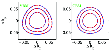
The band structures obtained from our TB model are plotted in Fig. 1 along with those obtained from DFT-HSE. The agreement in energies around both VBM and CBM for all three structures of MoS2 is excellent. Fig. 2 shows the energy contours around the valence band maximum (VBM) and the conduction band minimum (CBM) for the monolayer MoS2. Again, we observe excellent agreement in the shape of the energy contours from DFT-HSE and TB fitting. The band gap energies for different transitions and the effective mass values at different symmetry points obtained from the TB model are presented in Table 1 and Table 2 respectively. For the band gap energies a fitting accuracy of less than is achieved. On the other hand, for the effective masses, in most cases the deviations between the DFT-HSE and the TB values are less than which is quite acceptable. In four cases (excluding the monolayer structure) the deviations are higher with the worst situation at . Given that just a single set of TB parameters is used to produce the band structurues of all three different forms of the material, this level of quantitative consistency is rather satisfactory.
| Electron | Hole | ||||||
|---|---|---|---|---|---|---|---|
| Structure | Point | HSE (target) | TB (fitted) | Deviation (%) | HSE (target) | TB (fitted) | Deviation (%) |
| Monolayer | Kl | 0.407 | 0.430 | 4.58 | 0.485 | 0.463 | 4.54 |
| Kt | 0.404 | 0.426 | 5.45 | 0.480 | 0.458 | 4.58 | |
| Bilayer | 1.039 | 1.321 | 27.91 | ||||
| Kl | 0.430 | 0.457 | 6.28 | ||||
| Kt | 0.423 | 0.454 | 7.33 | ||||
| Bulk | 0.785 | 0.917 | 16.82 | ||||
| 0.574 | 0.712 | 24.04 | |||||
| 0.819 | 0.999 | 21.98 | |||||
| S | 7.6595 | -2.1537 | 8.7689 | 0.2129 | ||||
|---|---|---|---|---|---|---|---|---|
| Mo | 5.5994 | 6.7128 | 2.6429 | 1.0675 | ||||
| (S,Mo) | (S,S) | (S,S) | (Mo,Mo) | (S,Mo) | (S,S) | (S,S) | (Mo,Mo) | |
| -0.0917 | 0.3093 | 0.3207 | 0.1768 | 0.0294 | -0.0532 | -0.1430 | -0.0575 | |
| 0.6656 | -0.9210 | -0.1302 | 1.0910 | 0.1042 | 0.0240 | 0.0196 | 0.0057 | |
| -1.6515 | 0.1765 | |||||||
| 1.4008 | 0.7132 | 0.7053 | -0.3842 | -0.1865 | 0.0478 | -0.0486 | 0.0296 | |
| -0.4812 | -0.1920 | -0.0980 | 0.5203 | 0.0303 | -0.0104 | 0.0117 | 0.0946 | |
| 0.2177 | -0.2016 | 0.1164 | -0.5635 | -0.0480 | 0.0946 | 0.0297 | -0.1082 | |
| -1.0654 | -0.1432 | |||||||
| -2.8732 | -0.5204 | -0.0334 | -0.2316 | 0.0942 | 0.0724 | -0.0087 | 0.0212 | |
| 2.1898 | 0.2002 | |||||||
| 0.7739 | -0.1203 | -0.0370 | 0.0582 | 0.0132 | 0.0772 | -0.0031 | -0.0448 | |
| -1.9408 | -0.2435 | |||||||
| -3.1425 | 0.8347 | -0.2300 | 0.3602 | 0.0273 | 0.1849 | 0.0060 | -0.0216 | |
| 2.4975 | 0.7434 | 0.0050 | 0.0432 | 0.1940 | -0.0429 | -0.0378 | -0.0285 | |
| -0.3703 | -0.1919 | -0.1104 | 0.1008 | 0.1261 | -0.0333 | 0.0007 | 0.0432 |
In conclusion, we have developed a generic TB model for accurately calculating the band structures of bulk, monolayer and bilayer MoS2. Our TB model is based on the Slater-Koster method. For the optimization of the TB parameters, accurate target band structures are obtained using the screened hybrid DFT method. The accuracy of our TB model is verified by comparing the band gaps for different transitions and the effective masses at different band edges against the ab initio band structures. One main feature of our TB model is that with only one set of parameters it can reproduce the band structures of MoS2 of different structural configurations: from bulk to 2D structures. Our tight-binding model can be easily extended to other TMDC materials that show electronic characteristics similar to MoS2. The TB model reported in this paper is useful for simulations of quantum transport in nanoelectronic devices based on the TMDC materials.
Acknowledgements. This work is supported by the University Grant Council (Contract No. AoE/P-04/08) of the Government of HKSAR (FZ, JW), NSERC (HG) and IRAP (LL, YZ) of Canada. F.Z. would like to thank Dr. Ji Wei and Mr. Darshana Wickramaratne for useful discussions on the VASP calculations.
References
- (1) K. F. Mak, C. Lee, J. Hone, J. Shan, and T. F. Heinz, Phys. Rev. Lett. 105, 136805 (2010).
- (2) B. Radisavljevic, A. Radenovic, J. Brivio, V. Giacometti, and A. Kis, Nat. Nanotechnol. 6, 147 (2011).
- (3) H. Liu and P. D. Ye, IEEE Electron Dev. Lett. 33, 546 (2012).
- (4) Y. Yoon, K. Ganapathi, and S. Salahuddin, Nano Lett. 11, 3768 (2011).
- (5) L. Liu, S. B. Kumar, Y. Ouyang, and J. Guo, IEEE Trans. Electron Dev. 58, 3042 (2011).
- (6) K. Alam and R. K. Lake, IEEE Trans. Electron Dev. 59, 3250 (2012).
- (7) R. C. Bowen, G. Klimeck, R. Lake, W. R. Frensley, and T. Moise, J. Appl. Phys. 81, 3207 (1997).
- (8) M. Usman, H. Ryu, I. Woo, D. S. Ebert, and G. Klimeck, IEEE Trans. Nanotechnol. 8, 330 (2009).
- (9) M. Luisier and G. Klimeck, Phys. Rev. B, 80, 155430 (2009).
- (10) U. E. Avci, S. Hasan, D. E. Nikonov, R. Rios, K. Kuhn, I. A. Young, Symp. VLSI Tech., pp. 183 (2012).
- (11) J. Heyd, G. E. Scuseria, and M. Ernzerhof, J. Chem. Phys. 118, 8207 (2003); 124, 219906 (2006).
- (12) Y.-S. Kim, K. Hummer, and G. Kresse, Phys. Rev. B 80, 035203 (2009).
- (13) Y.-S. Kim, M. Marsman, and G. Kresse, Phys. Rev. B 82, 205212 (2010).
- (14) J. E. Peralta, J. Heyd, and G. E. Scuseria, Phys. Rev. B 74, 073101 (2006).
- (15) T. Cheiwchanchamnangij and W. R. L. Lambrecht, Phys. Rev. B 85, 205302 (2012).
- (16) J. K. Ellis, M. J. Lucero,1 and G. E. Scuseria, Appl. Phys. Lett. 99, 261908 (2011).
- (17) H. Peelaers and C. G. Van de Walle, Phys. Rev. B 86, 241401(R) (2012).
- (18) G. Kresse and J. Hafner, Phys. Rev. B 47, R558 (1993); G. Kresse and J. Furthmuller, Phys. Rev. B 54, 11169 (1996).
- (19) J. P. Perdew, K. Burke, and M. Ernzerhof, Phys. Rev. Lett. 77, 3865 (1996).
- (20) T. Bucko, J. Hafner, S. Lebegue, and J. G. Angya, J. Phys. Chem. A 114, 11814 (2010).
- (21) A. R. Beal and H. P. Hughes, J. Phys. C 12, 881 (1979).
- (22) Nanoskif is a special tool developed by NanoAcademic Technologies Inc. (www.nanoacademic.com) for the optimization of the Slater-Koster energies and/or overlap integrals used in the tight-binding models by fitting a target band structure of a system, or a set of band structures of several systems simultaneously, employing state-of-the-art algorithms.
- (23) J. C. Slater and G. F. Koster, Phys. Rev. 94, 1498 (1954).
- (24) D. J. Chadi, Phys. Rev. B 16, 790 (1977).