Characterization and Suppression of Low-frequency Noise in Si/SiGe Quantum Point Contacts and Quantum Dots
Abstract
We report on the effects of a global top gate on low-frequency noise in Schottky gate-defined quantum point contacts (QPCs) and quantum dots (QDs) in a modulation-doped Si/SiGe heterostructure. For a relatively large top gate voltage, the QPC current shows frequent switching with Lorentzian type charge noise. As the top gate voltage is decreased, the QPC pinch-off voltage becomes less negative, and the noise becomes rapidly suppressed in a homogeneous background noise. We apply this top-gating technique to double QDs to stabilize the charge state for the electron number down to zero.
Coherent control of single electron spin in solids aiming towards the realization of fundamental devices for quantum computation has been performed extensively in GaAsPetta et al. (2005); Koppens et al. (2006); Nowack et al. (2007); Pioro-Ladrière et al. (2008); Brunner et al. (2011); Shulman et al. (2012) and more recently in SiMaune et al. (2012); Pla et al. (2012) as well. Si quantum dots (QDs) are one of the most promising candidates for implementing scalable spin quantum bit (qubit) systems because of the long coherence time due to weak spin-orbit and hyperfine interactions. Recent experiments on Si QDs have shown the relaxation time and the dephasing time much longer than those observed for GaAs QDs.Simmons et al. (2011); Prance et al. (2012); Maune et al. (2012) However, at present the realization of stable QDs in a two-dimensional electron gas (2DEG) at a modulation-doped Si/SiGe heterostructure is still challenging due to the problem of charge noise which cause sudden changes to the QD states.Wild et al. (2010); Payette et al. (2012) To realize stable qubit operation it is necessary to characterize and reduce the charge noise in quantum point contacts (QPCs) which form tunnel junctions with the QD.
Charge noise in gate-defined QPCs has been studied in detail for modulation-doped GaAs/AlGaAs heterostructures using techniques of asymmetrically biasing gatesSakamoto et al. (1995), bias-coolingPioro-Ladrière et al. (2005), top gate biasingBuizert et al. (2008) and combinations of them. In Ref. Sakamoto et al. (1995) they observed charge noise caused by thermally activated trapping and detrapping by charge traps in local potential minima formed near the QPC channel when Schottky gates were occasionally biased to align the energy level of the charge trap and Fermi level of the QPC channel. On the other hand, in Ref. Pioro-Ladrière et al. (2005); Buizert et al. (2008), the charge noise is attributed to the electron tunneling between the surface and the 2DEG via charge traps in between. They observed strong charge noise reduction by application of bias-cooling or top gate technique which makes the operation voltage of the surface Schottky gate less negative. Then the tunnel rate of electrons from the Schottky gate to the QPC channel via charge traps or most probably ionized donor states (discussed later) is reduced to improve the charge stability. For Si/SiGe Schottky gated devices, both mechanisms can also be considered as noise sources.
The top gate-biasing may be useful to reduce the charge noise in Si/SiGe devices, but not the bias cooling because -type donors in SiGe do not have deep levels like DX centers Buks et al. (1994) in -doped AlGaAs. It has been demonstrated for Si/SiGe QPCs defined by gate electrodes placed on a Al2O3 insulated Si surface, i.e., metal-oxide-semiconductor (MOS), that negatively biasing a global top gate gradually reduces the charge noise in the conductance.Wild et al. (2012) The charge noise may be more significant in surface Schottky gate structures than in MOS gate structures because there is no direct leakage between the gate metal and the QPC channel in the latter, but no detailed studies on charge noise spectra in Si/SiGe QPCs have been reported to date.
In this letter, we characterize low-frequency charge noise spectra in Schottky gated Si/SiGe QPCs with a global top gate voltage. We observe a strong reduction in the component in the charge noise by negatively biasing the top gate. We then apply this technique to enable stable operation of double QDs and finally achieve stable charge state with just a few electrons.

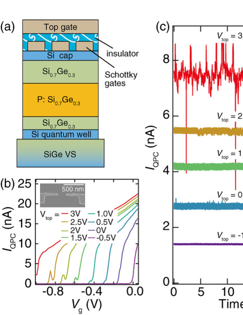
The Si/SiGe heterostructure used in this study is grown by ultra-high vacuum chemical vapor deposition. The heterostructure configuration is shown in Fig. 1(a). First a 3 thick graded buffer is grown on a Si substrate by linearly increasing the Ge content from 0 % to 30 %, and then a 1 thick Si0.7Ge0.3 buffer is grown. A 15 nm thick Si quantum well, a 10 nm thick undoped Si0.7Ge0.3 spacer, a 25 nm thick phosphorous doped Si0.7Ge0.3, a 20 nm thick undoped Si0.7Ge0.3 cap, and finally a 7.5 nm thick Si cap are successively grown on the buffer. The resulting 2DEG has an electron density of 2.3 1011 cm-2 and a mobility of 1.3 105 cm2/Vs at mK.
The stack of gate electrodes is also shown in Fig. 1(a). Ohmic contacts to the 2DEG are achieved by Au/Sb evaporation and subsequent annealing. QPCs are formed by Pd Schottky gates on the Si cap layer surface by a standard electron-beam lithography technique. The top gate which covers the whole active QPC area is placed on top of the surface gates with cross-linked PMMA as an insulator in between.
Figure 1(b) shows the QPC current v.s. surface gate voltage measured for various top gate voltages at K. The QPC pinch-off voltage becomes less negative as is decreased. Figure 1(c) shows time traces measured for various . The Schottky gate is biased at a condition where the slope of QPC current () is largest to maximize the charge sensitivity. It is clear that both magnitude and frequency of the current fluctuation become significantly small as the top gate is made less positive or negative. The minimum top gate voltage that we can apply in this sample is V, because the QPC conductance rapidly quenches for V.
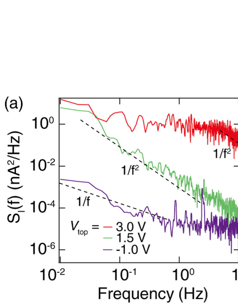
Next we analyze power spectra of the charge noise using fast Fourier transform (FFT) of time traces. Figure 2(a) shows FFT power spectra of in the low-frequency range of to 10 Hz measured for various . The shows a behavior known as two-level Lorentzian type fluctuation van der Ziel (1986) at relatively large . In this condition charge fluctuations due to just a few charge traps near the QPC channel are dominant in the noise characteristic. On the other hand, as the is made less positive, the noise is rapidly suppressed and disappear in the type homogeneous background charge noise which comes from summation of many trapping sites. van der Ziel (1986) To more quantitatively characterize the noise feature, we analyze the integrated spectral density over a finite frequency range to derive the mean value of the gate voltage fluctuation amplitude, of the noise as in ref Buizert et al. (2008); S.W.Jung et al. (2004)
| (1) |

Here is the background noise measured at V. We derive it for a frequency range of 0.01 to 49 Hz to avoid a relatively large 50 Hz noise which comes from measurement instruments. The obtained shown in Fig. 2(b) changes exponentially as a function of . This is similar to that in a previous report on GaAs QPCs, but the residual seems nearly one order larger than that of GaAs QPCs.Buizert et al. (2008) We believe further reduction of the charge noise level can be achieved by optimization of the heterostructure and gating technique.

The charge noise reduction observed in our Si/SiGe system can be explained by considering surface - 2DEG tunneling which has already been confirmed in GaAs devices.Pioro-Ladrière et al. (2005); Buizert et al. (2008) In usual depletion type devices, application of less positive or more negative voltage to the top gate makes less negative the surface Schottky gate voltage to pinch off the QPC channel, and therefore the gate leakage current is reduced due to reduced electron tunneling between the surface and the channel. We exclude trapping and detrapping of charge traps near the QPC channel from the reason for the charge noise because the observed charge noise decreases monotonically, but not resonantly when the top gate voltage is reduced. It may be reasonable to assign the charge traps to modulation doped ionized impurities because recent report on an undoped Si/SiGe heterostructure has shown a significant improvement in the charge stability.Borselli et al. (2011)
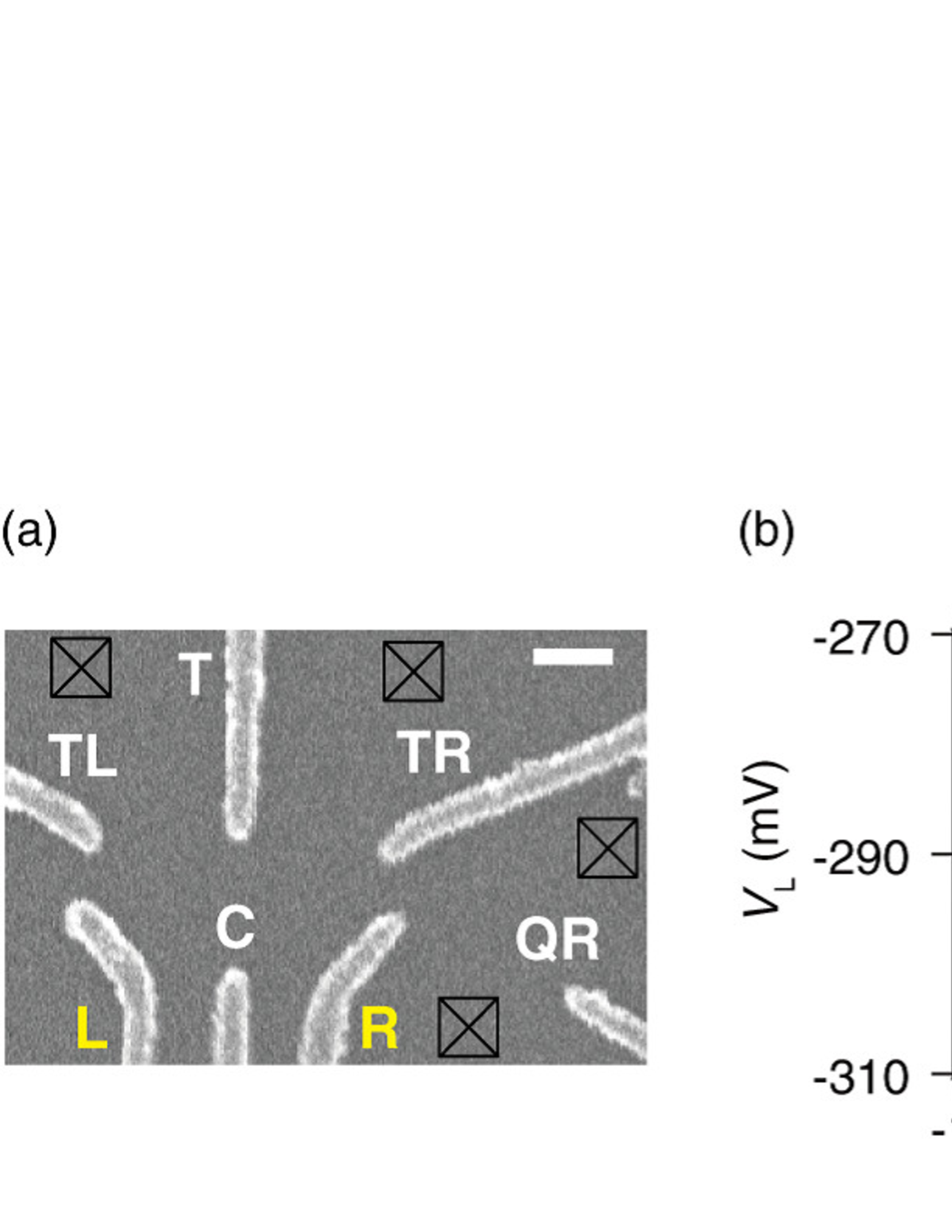
Finally we prepare a double QD in the same Si/SiGe heterostructure defined by the same gating technique and measure the stability diagram using the top gate voltage as one parameter. Figure 3(a) shows the scanning electron micrograph of the double QD. The charge state of the double QD is monitored using a proximal QPC as a charge sensor. The measured stability diagram in the plane of two side gate voltages and is shown in Fig. 3 measured at V (b) and V (c), respectively. The gray scale indicates the numerical derivative of the charge sensor conductance with . The surface gate geometry is designed to have a relatively small gap in each QPC so that only a small positive voltage is applied to the top gate to form a double QD. The double QD is depleted to the (0, 0) charge configuration by adjusting and . The (0, 0) state is confirmed because any extra charge transition line is observed for more negative gate voltages. In Fig. 3(b) charge state transition lines between the dot and 2DEG leads and between two dots are unclear due to electrostatic potential fluctuations by charge noise. In contrast, in Fig. 3(c) all charge state transition lines are better defined, while the operation voltages of the Schottky gates are not so different between Fig 3 (b) and Fig 3 (c). Note that the surface to 2DEG tunneling via charge traps can be reduced even without significant changes in the surface Schottky gate voltage because the energy level of the charge traps relative to the Fermi level of the gate metal can be modified just by application of the top gate voltage.
In summary, we have fabricated surface Schottky gate defined QPCs and double QDs in Si/SiGe heterostructures with a global top gate to study the top gate effect on the charge noise.
We measured the real time current noise and noise power spectra for the QPCs and observed that switching noise is rapidly suppressed and finally disappear in the noise background as the top gate voltage is made less positive or more negative.
This result is similar to that reported for clean GaAs QPCsBuizert et al. (2008).
For the double QD, we also observed a similar effect of the top gate to stabilize the charge state with reduced charged noise.
We could finally achieve a few-electron double QD with no notable switching noise.
This top gate technique will be useful to stabilize the gate performance in Si/SiGe QDs
and eliminate dephasing of qubits due to charge noise via exchange interaction. Culcer et al. (2009)
We gratefully thank Juergen Sailer, Andreas Wild, Dominique Bougeard, and Gerhard Abstreiter for helpful discussions. This work was financially supported by GCOE for Physical Sciences Frontier, MEXT, Japan, Project for Developing Innovation Systems of the Ministry of Education, Culture, Sports, Science and Technology, MEXT, Japan, Grant-in-Aid for Scientific Research on Innovative Areas (21102003), MEXT, Japan, and Funding for World-Leading Innovative R&D on Science and Technology (FIRST) Program, Japan.
References
- Petta et al. (2005) J. R. Petta, A. C. Johnson, J. M. Taylor, E. A. Laird, A. Yacoby, M. D. Lukin, C. M. Marcus, M. P. Hanson, and A. C. Gossard, Science 309, 2180 (2005).
- Koppens et al. (2006) F. H. L. Koppens, C. Buizert, K. J. Tielrooij, I. T. Vink, K. C. Nowack, T. Meunier, L. P. Kouwenhoven, and L. M. K. Vandersypen, Nature 442, 766 (2006).
- Nowack et al. (2007) K. C. Nowack, F. H. L. Koppens, Y. V. Nazarov, and L. M. K. Vandersypen, Science 318, 1430 (2007).
- Pioro-Ladrière et al. (2008) M. Pioro-Ladrière, T. Obata, Y. Tokura, Y.-S. Shin, T. Kubo, K. Yoshida, T. Taniyama, and S. Tarucha, Nat. Phys. 4, 776 (2008).
- Brunner et al. (2011) R. Brunner, Y.-S. Shin, T. Obata, M. Pioro-Ladrière, T. Kubo, K. Yoshida, T. Taniyama, Y. Tokura, and S. Tarucha, Phys. Rev. Lett. 107, 146801 (2011).
- Shulman et al. (2012) M. D. Shulman, O. E. Dial, S. P. Harvey, H. Bluhm, V. Umansky, and A. Yacoby, Science 336, 202 (2012).
- Maune et al. (2012) B. M. Maune, M. G. Borselli, B. Huang, T. D. Ladd, P. W. Deelman, K. S. Holabird, A. A. Kiselev, I. Alvarado-Rodriguez, R. S. Ross, A. E. Schmitz, M. Sokolich, C. A.Watson, M. F. Gyure, and A. T. Hunter, Nature 481, 344 (2012).
- Pla et al. (2012) J. J. Pla, K. Y. Tan, J. P. Dehollain, W. H. Lim, J. J. L. Morton, D. N. Jamieson, A. S. Dzurak, and A. Morello, Nature 489, 541 (2012).
- Simmons et al. (2011) C. B. Simmons, J. R. Prance, B. J. V. Bael, T. S. Koh, Z. Shi, D. E. Savage, M. G. Lagally, R. Joynt, M. Friesen, S. N. Coppersmith, and M. A. Eriksson, Phys. Rev. Lett. 106, 156804 (2011).
- Prance et al. (2012) J. R. Prance, Z. Shi, C. B. Simmons, D. E. Savage, M. G. Lagally, L. R. Schreiber, L. M. K. Vandersypen, M. Friesen, R. Joynt, S. N. Coppersmith, and M. A. Eriksson, Phys. Rev. Lett. 108, 46808 (2012).
- Payette et al. (2012) C. Payette, K. Wang, P. J. Koppinen, Y. Dovzhenko, J. C. Sturm, and J. R. Petta, Appl. Phys. Lett. 100, 043508 (2012).
- Wild et al. (2010) A. Wild, J. Sailer, J. Nutzel, G. Abstreiter, S. Ludwig, and D. Bougeard, New J. Phys. 12, 113019 (2010).
- Sakamoto et al. (1995) T. Sakamoto, Y. Nakamura, and K. Nakamura, Appl. Phys. Lett. 67, 2220 (1995).
- Pioro-Ladrière et al. (2005) M. Pioro-Ladrière, J. H. Davies, A. R. Long, A. S. Sachrajda, L. Gaudreau, P. Zawadzki, J. Lapointe, J. Gupta, Z. Wasilewski, and S. Studenikin, Phys. Rev. B 72, 115331 (2005).
- Buizert et al. (2008) C. Buizert, F. H. L. Koppens, M. Pioro-Ladrière, H.-P. Tranitz, I. T. Vink, S. Tarucha, W. Wegscheider, and L. M. K. Vandersypen, Phys. Rev. Lett. 101, 226603 (2008).
- Buks et al. (1994) E. Buks, M. Heiblum, Y. Levinson, and H. Shtrikman, Semicond. Sci. Technol. 9, 2031 (1994).
- Wild et al. (2012) A. Wild, J. Kierig, J. Sailer, I. J. W. Ager, E. E. Haller, G. Abstreiter, S. Ludwig, and D. Bougeard, Appl. Phys. Lett. 100, 143110 (2012).
- van der Ziel (1986) A. van der Ziel, Noise in Solid State Devices and Circuits (Wiley, New York, 1986).
- S.W.Jung et al. (2004) S.W.Jung, T.Fujisawa, Y.H.Jeong, and Y.Hirayama, Appl. Phys. Lett. 85, 768 (2004).
- Borselli et al. (2011) M. G. Borselli, K. Eng, E. T. Croke, B. M. Maune, B. Huang, R. S. Ross, A. A. Kiselev, P. W. Deelman, I. Alvarado-Rodriguez, A. E. Schmitz, M. Sokolich, K. S. Holabird, T. M. Hazard, M. F. Gyure, and A. T. Hunter, Appl. Phys. Lett. 99, 063109 (2011).
- Hanson et al. (2007) R. Hanson, L. P. Kouwenhoven, J. R. Petta, S. Tarucha, and L. M. K. Vandersypen, Rev. Mod. Phys. 79, 1217 (2007).
- Culcer et al. (2009) D. Culcer, X. Hu, and S. Sarma, Appl. Phys. Lett. 95, 073102 (2009).