Graphene-based charge sensors
Abstract
We discuss graphene nanoribbon-based charge sensors and focus on their functionality in the presence of external magnetic fields and high frequency pulses applied to a nearby gate electrode. The charge detectors work well with in-plane magnetic fields of up to 7 T and pulse frequencies of up to 20 MHz. By analyzing the step height in the charge detector’s current at individual charging events in a nearby quantum dot, we determine the ideal operation conditions with respect to the applied charge detector bias. Average charge sensitivities of can be achieved. Additionally, we investigate the back action of the charge detector current on the quantum transport through a nearby quantum dot. By setting the charge detector bias from 0 to 4.5 mV, we can increase the Coulomb peak currents measured at the quantum dot by a factor of around 400. Furthermore, we can completely lift the Coulomb blockade in the quantum dot.
I Introduction
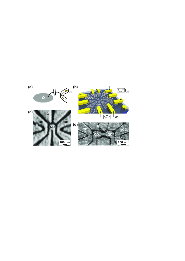
Charge sensors play an important role in low-dimensional electronic circuits, where detecting changes of localized charge states are crucial and challenging tasks. In fact, nanoelectronic systems i.e. electronic systems with reduced dimensions show a variety of interesting physics including Coulomb blockade Kou97 , Kondo effect Gol98 or Fano resonances Joh04 , all closely related to the localization of electronic charge. Read out and manipulation of isolated electrons are key elements for studying and exploiting these phenomena. Along this line charge detectors based on quantum point contacts (QPCs) Wee88 have extensively been used in two dimensional electron systems Fie93 . In particular III/V heterostructures have been used as host materials for QPCs. In such devices coherent spin and charge manipulation Hay03 ; Pet05 , full counting statistics Gus06 , time resolved charge detection Gus06 ; Fuj06 and controllable coupling to different quantum devices Elz04 ; Shi09 ; Fre12 have been demonstrated. Moreover, QPC-based charge detectors are regularly used to read out spin qubits realized in double quantum dot systems in GaAs/AlGaAs heterostructures Elz03 ; Blu10 ; Now11 ; Shu12 . In these experiments the charge detection fidelity is of great interest in order to maximize the read out speed. The detection fidelity can be optimized by increasing the pinch-off slope and the capacitance between the QPC and the investigated device. While the capacitance can be tuned by reducing the distance between the charge detector and the system of interest (see illustration in Fig. 1(a)), the slope can be increased by replacing the QPC by a single electron transistor (SET). Recently, the use of charge detectors has been extended to hybrid systems where for example a nanowire quantum dot was probed by an underlying QPC detector Cho12 ; Shu08 or a metallic SET was used to detect charging events on a carbon nanotube quantum dot Got08 .
More recently, it has also been shown that narrow graphene ribbons can be used as well-working charge detectors Gue08 . This approach has been employed to perform charge sensing on individual graphene quantum dots Gue08 ; Mue12 ; Wan10 ; Fri11 ; Vol13 , including time resolved detection of charging events on such systems Gue11 . Additionally, a carbon nanotube-graphene hybrid device has recently been demonstrated where the charge state of a carbon nanotube quantum dot can be detected by the current through a nearby graphene nanoribbon-based charge sensor Eng13 .
In particular, graphene attracted increasing interest in the last years, which is mainly due to its remarkable electronic properties such as high carrier mobilities, suppression of direct backscattering and low intrinsic spin noise, which makes graphene an interesting candidate for future electronics and quantum information technology Tra07 ; Los98 . For example, graphene based quantum dots (QD) promise weaker hyperfine coupling as well as weaker spin orbit interaction compared to state-of-the-art III/V heterostructure devices Min06 ; Hue06 . A key challenge when creating graphene based electronic devices is the absence of a band gap in this material and the phenomenon of Klein tunneling, making it difficult to electrostatically confine electrons Kat06 . However, structuring graphene on sub-micron scales yields a possibility to overcome this problem as a mainly disorder dominated energy gap opens Han07 ; Sta09 ; Liu09 ; Gal10 ; Han10 ; Ter11 . Thus, graphene nanoribbons, single-electron-transistors, QDs and double quantum dots have been successfully fabricated and investigated over the past years Tod09 ; Ihn10 ; Sta08 ; Pon08 ; Mos10 ; Vol11 ; Gue12 . Furthermore, it has been shown that it is possible to fabricate graphene quantum dots with integrated graphene nanoribbon-based charge detectors in a single fabrication step Gue11 leading to a more reliable and reproducible fabrication technology for potentially high quality charge sensors.
In this article, we discuss the fabrication of graphene nanoribbon-based charge detectors (section II) and characterize their behaviour in transport measurements (section III). We show that the charge detector retains its functionality under applying of a magnetic fields and square voltage pulses on a nearby graphene side gate. Finally, we investigate back action effects of the charge detector on a probed graphene QD.
II Device fabrication
The device fabrication is based on mechanical exfoliation of natural graphite. The ultra-thin graphite flakes are placed on an insulating 290 nm thick silicon oxide (SiO2) layer on top of highly doped silicon (Si++). To identify graphene flakes optical microscopy complemented by Raman spectroscopy is employed Fer06 ; Gra07 . Individual graphene flakes are subsequently nanostructured by electron beam lithography (EBL) and reactive ion etching (RIE) with an Ar/O2 plasma Mol07 . The graphene nanostructures are contacted by an additional EBL step followed by metalization and lift-off (see illustration in Fig. 1(b)). Our contacts consist of 5 nm Cr and 50 nm Au. In Figs. 1(c) and 1(d) we show two scanning force microscope (SFM) images of both, (c) a graphene quantum dot (QD), and (d) a double quantum dot device with integrated graphene charge detectors (CDs). In both devices the charge detectors are capacitively coupled to a graphene island hosting localized electrons.
Here, we will mainly focus on graphene CDs coupled to graphene single quantum dot structures as depicted in Figs. 1(b) and 1(c). Our graphene QDs have diameters of around 100 nm and they are connected to source and drain leads by narrow graphene constrictions which act as tunable tunneling barriers Sta08 . Two nanoribbons with a width of about 70 nm, located at either side of the QD, act as charge detectors. By applying a reference potential to the graphene charge detectors, they can also be used as lateral gates, especially for tuning the transparency of the tunneling barriers. Additional plunger gates (PG) allow to electrostatically tune the QD potential as well as the tunneling rates. The highly doped Si substrate acts as a back gate and can be employed to tune the overall Fermi level in the graphene device.
III Measurements and discussion
All transport measurements presented in this article are performed in a dilution refrigerator with a base temperature below 20 mK. Home built amplifiers are used to detect currents with noise levels of around 10 fA/. For the pulse gating experiments a Tektronix AWG 7082C is used to provide rectangular pulses with rise times of about 250-300 ps.
III.1 Device characterization
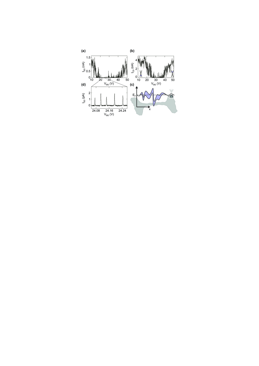
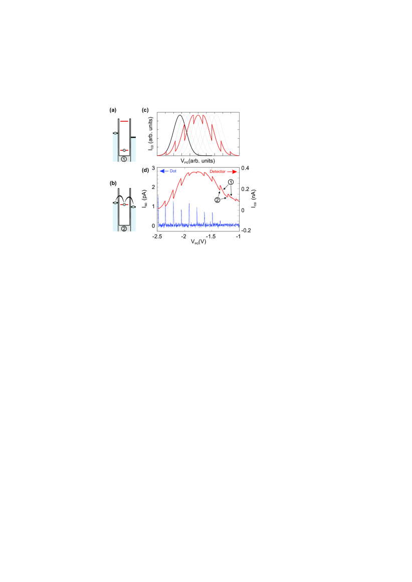
In Figs. 2(a) and 2(b) we show the transport characteristics of a graphene quantum dot and a graphene nanoribbon and quantum dot on a large energy, i.e. large back gate voltage range, respectively. Here, the current is measured while varying the back gate voltage from 10 to 50 V. For small back gate voltages both devices show hole-dominated transport, while for large back gate voltages the transport is electron-dominated (see also insets in Fig. 2(b)). These two regions are separated by the so-called transport gap, where the measured current is strongly suppressed. The transport gap is located at positive gate voltages (around 20 to 37 V in Fig. 2(a) and 27 to 37 V in Fig. 2(b)) indicating a significant p-doping of both structures, which is commonly observed in etched graphene nanostructures Ter11 ; Gue12 . This p-doping arises most likely due to polymer resist residues and/or oxygen atoms bound to the graphene edges coming from the Ar/O2 plasma etching process Ryu10 . In the transport gap regime the electronic transport is dominated by stochastic Coulomb blockade where lateral confinement in combination with a significant disorder potential, arising from both (i) bulk disorder and (ii) edge roughness, play an important role (see illustration in Fig. 2(c)) Sta09 ; Mol10 . The observed large-scale current fluctuations inside the gap region originate from local resonances in the graphene constriction. In Fig. 2(d) we show a close up of the back gate characteristics of the graphene QD inside the transport gap, highlighting individual Coulomb resonances. Transport is blocked if no QD state is aligned inside the bias window (Coulomb blockade, see Fig. 3(a)). Individual Coulomb resonances are observed if a state is aligned between the chemical potentials of the source and drain leads (Fig. 3(b)).
Individual conductance resonances in the transport characteristics of a graphene nanoribbon can be used to detect charging events on a capacitively coupled QD close by. Whenever the overall charge of the QD changes, the electrostatic potential in the nanoribbon-based charge detector is shifted which results in a conductance step of the CD (Fig. 3(c)). Thus, individual charging events in the QD can be probed by measuring the current passing through the nanoribbon, which consequently acts as a charge detector Gue08 ; Wan10 ; Fri11 . In Fig. 3(d) the simultaneously measured current through the quantum dot () and the charge detector () are shown as a function of the plunger gate voltage . The steps in are well aligned with the Coulomb peaks in . The CD can even resolve charging events that cannot be measured by the direct current since the Coulomb peaks vanish in the noise of the signal (see V in Fig. 3(d)).
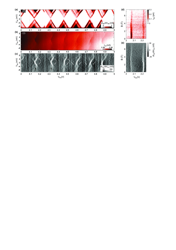
In Fig. 4 (a) we show so-called Coulomb diamonds in the differential conductance measured on the QD. Signatures of transport through excited states in the QD are observed as faint lines running parallel to the diamond edges. The CD signal in Figs. 4(b) and 4(c) shows features well aligned with the Coulomb resonances visible in Fig. 4(a). Interestingly, for the two left Coulomb diamonds (marked by the vertical black arrows in Fig. 4(c)) the dominant tunneling barrier changes when going from negative to positive , indicating a rather strong capacitive coupling of the QD tunnel barriers to the source and the drain lead. Apart from the ground state transport also transport via excited state transitions can be identified in the differential transconductance of the CD, highlighted by white arrows.

III.2 Charge detection at finite magnetic fields and pulsed-gates
Next we demonstrate that the graphene nanoribbon-based CD also works over a large range of external magnetic fields. This is important for detecting individual spin states in graphene QDs. Please note that it has been shown that magnetic fields may strongly alter the transport properties of graphene nanoribbons Gue11a , rendering this a non-trivial task. In Fig. 4(d) two Coulomb resonances are measured for an in-plane magnetic field range of 0 to 7.4 T. Both resonances are also present in the transconductance in Fig. 4(e) with similar resolution. So far, all results have been obtained from DC measurements. In the measurements shown in Fig. 5, a pulsed-gate technique was used to manipulate the transport through the QD on nanosecond time scales Fuj01 ; Dro12 ; Vol13 . In these measurements a rectangular pulse applied to the plunger gate (see ”PG” in Fig. 1(c)) located in the vicinity of the QD. Importantly, the voltage pulse shifts the QD potential by the electrostatic coupling. In Fig. 5(b) the evolution of a Coulomb resonance for increasing pulse amplitude at a constant frequency of 20 MHz is plotted. The Coulomb resonance splits into two peaks with increasing pulse amplitude. The equivalent height of the two peaks after splitting is in good agreement with the pulse duty cycle of 50% (see Fig. 5(b)). This splitting is also observed in the charge detector transconductance as shown in Fig. 5(c).
III.3 Back action
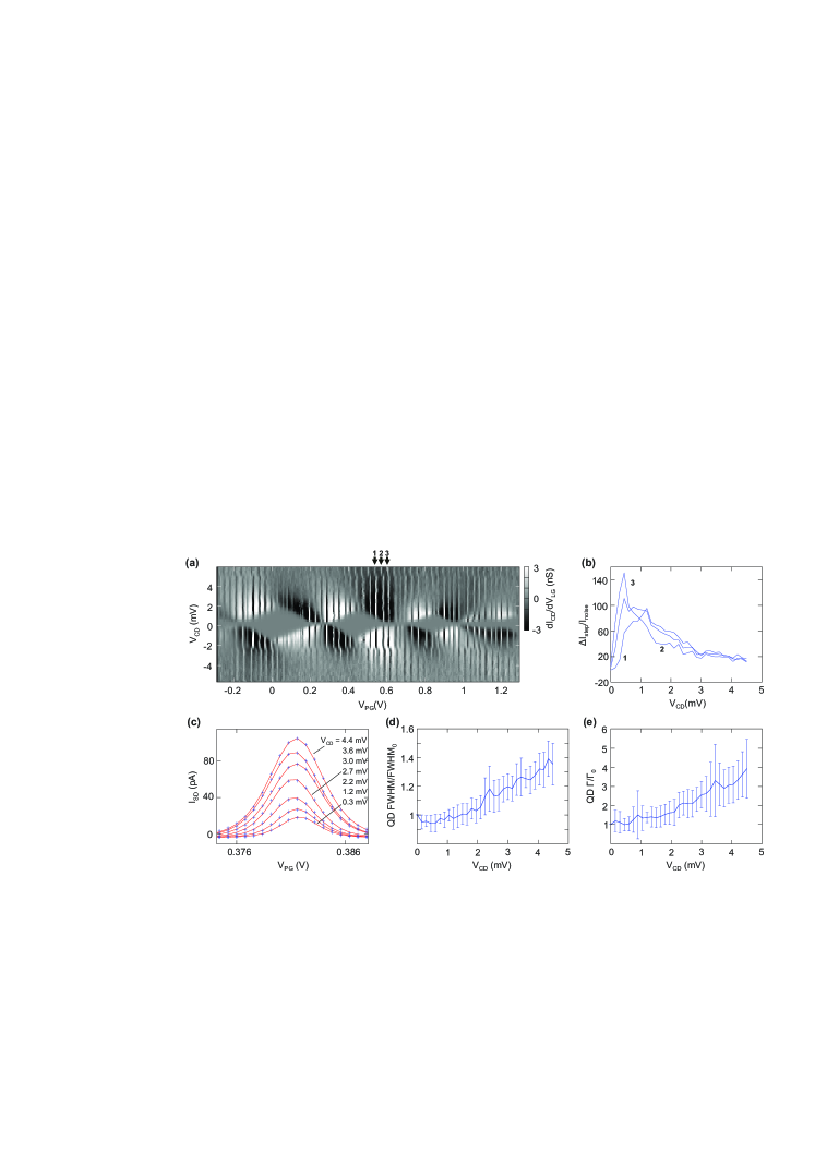
In the measurements discussed in the previous sections the charge detection bias () was set such that charging events in the QD could be easily detected. In the following we will investigate (i) the influence of the CD bias voltage on the detection sensitivity as well as (ii) the back action of the detection on the transport through the quantum dot. In Fig. 6(a) we show the transconductance of the detector measured as function of detector bias () and plunger gate voltage. Remarkably, for small bias voltages we observe well-resolved Coulomb diamonds with charging energies on the order of 1.5 meV. This is in perfect agreement with the nature of the resonances in the charge detector nanoribbon. Inside the diamonds, where transport through the nanoribbon is (Coulomb) blocked the CD is completely insensitive to charging events in the nearby QD.
In order to detect QD states over an extended range the CD must be operated at a bias value outside the Coulomb blockade regime. However, increasing leads to an overall increased current through the CD. This broadens the CD resonances, which results in a decreasing signal-to-noise ratio for detecting individual charging events. In Fig. 6(b) we show the signal-to-noise ratio of three conductance steps of the CD investigated for a range of 0 to 5 mV. The signal-to-noise ratio is best for low as long as the CD is not blocked due to Coulomb blockade. From Fig. 6(b) we extract an average charge sensitivity of at = 0.5 mV. Please note that the charge sensitivity strongly scales with and the slope of the CD resonance where the charging event in the QD occurs.
Furthermore, the transport through the QD is strongly affected by the charge detector current. The Coulomb resonances of the QD broaden with increasing charge detector bias which is due to back action effects. We phenomenologically investigate this behavior by fitting the Coulomb peak in the QD by , with the fit parameters , and to different Coulomb resonances located in the regime of = 0.3 to 0.5 V. An exemplary evolution of a Coulomb resonance with increasing is displayed in Fig. 6(c). Fig. 6(d) shows the FWHM averaged over 8 Coulomb resonances depending on . Varying from 0 to 4.5 mV increases the FWHM by around 50%. At the same time the average peak height rises by about 400% (see Fig. 6(e)). The strong back action of the CD onto the QD can also nicely be seen in Fig. 7, where the low-bias current through the QD is in log-scale plotted as function of and . With increasing the Coulomb resonances in the QD broaden until the Coulomb blockade is completely lifted.
This dependency on the current flowing through the CD indicates that the increase and broadening of the Coulomb resonances originate from noise and fluctuations in the CD nanoribbon Gue11 . Coupling of the nanoribbon to the QD via phonons seems less plausible as the phonons would have to couple via the SiO2 substrate due to the destroyed graphene lattice. Consequently, it is likely that photons play an important role and that processes related to photon assisted tunneling are responsible for lifting the Coulomb blockade in the transport through the graphene QD. In summary, the best conditions for charge sensing, i.e. for detecting individual charging events in the nearby QD found at slightly above the Coulomb blockade regime of the CD. In this case all QD resonances can be probed with a good signal-to-noise ratio, while the back action on the QD is kept small.

IV Conclusion
We have characterized graphene nanoribbon-based charge detectors. By bias spectroscopy measurements we have shown that excited states of a nearby quantum dot are resolved with the graphene charge detector. Furthermore, the charge detector was successfully tested in experimental setups where in plane magnetic fields up to more than 7 T and pulsed-gates at 20 MHz were used to manipulate individual QD states. We reach average charge sensitivities on the order of 1.3. The charge detector can be operated in regimes with high sensitivity, while the back action onto the investigated QD is kept at a minimum. However, at higher charge detector bias voltages, we observe complete lifting of the Coulomb blockade regime in the probed quantum dot. A detailed understanding of the graphene-based charge sensors may open new fields of applications, in particular in view of the truly two-dimensional nature of these sensors.
Acknowledgement
We acknowledge S. Trellenkamp for support with electron beam lithography and U. Wichmann for help with the low-noise measurement electronics. We thank F. Haupt, B. Terrés, and A. Epping for helpful discussions. Support by the DFG (SPP-1459 and FOR-912), JARA seed fund, and the ERC are gratefully acknowledged.
References
- (1) Kouwenhoven L P, Marcus C M, McEuen P L, Tarucha S, Westervelt R M, and Wingreen N S 1997, in Mesoscopic Electron Transport, edited by Sohn L L, Kouwenhoven L P, and Schön G Series E: Applied Sciences (Kluwer Academic, Dordrecht), 345, 105 214
- (2) Goldhaber-Gordon D, Shtrikman H, Mahalu D, Abusch-Magder D, Meirav U, and Kastner M A 1998 Kondo effect in a single-electron transistor. Nature 391 156
- (3) Johnson A C, Marcus C M, Hanson P, and Gossard A C 2004 Coulomb-Modified Fano Resonance in a One-Lead Quantum Dot Phys. Rev. Lett. 93 106803
- (4) van Wees B, van Houten H, Beenakker C W J, Williamson J G, Kouwenhoven L P, van der Marel D, and Foxon C T 1988 Quantized conductance of point contacts in a two-dimensional electron gas. Phys. Rev Lett. 60 848
- (5) Field M, Smith C G, Pepper M, Ritchie D A, Frost J E F, Jones G A C, and Hasko D G 1993 Measurements of Coulomb Blockade with a Noninvasive Voltage Probe. Phys. Rev. Lett. 70 1311
- (6) Petta JR, Johnson A C, Taylor J M, Laird E A, Yacoby A, Lukin M D, Marcus C M, Hanson M P, and Gossard A C 2005 Coherent Manipulation of Coupled Electron Spins in Semiconductor Quantum Dots. Science 309 2180
- (7) Hayashi T, Fujisawa T, Cheong HD, Jeong YH, and Hirayama Y 2003 Coherent Manipulation of Electronic States in a Double Quantum Dot. Phys. Rev. Lett. 91 226804
- (8) Gustavsson S, Leturcq R, Simovic B, Schleser R, Ihn T, Studerus P, and Ensslin K 2006 Counting Statistics of Single Electron Transport in a Quantum Dot. Phys. Rev. Lett. 96 076605
- (9) Fujisawa T, Hayashi T, Tomita R, and Hirayama Y 2006 Bidirectional Counting of Single Electrons. Science 312 1634
- (10) Elzermann J M, Hanson R, van Beveren L H W, Witkamp B, Vandersypen L M K, and Kouwenhoven L P 2004 Single-shot read-out of an individual electron spin in a quantum dot. Nature 430 431
- (11) Shinkai G, Hayashi T, Ota T, and Fujisawa T 2009 Correlated coherent oscillations in coupled semiconductor charge qubits. Phys. Rev. Lett. 103 056802
- (12) Frey T, Leek P J, Beck M, Blais A, Ihn T, Ensslin K, and Wallraff A 2012 Dipole Coupling of a Double Quantum Dot to a Microwave Resonator. Phys. Rev. Lett. 108 046807
- (13) Bluhm H, Foletti S, Neder I, Rudner M, Mahalu D, Umansky V, and Yacoby A 2010 Dephasing time of GaAs electron-spin qubits coupled to a nuclear bath exceeding 200 us. Nat. Phys. 7 109
- (14) Nowack K C, Shafiei M, Laforest M, Prawiroatmodjo G E D K, Schreiber L R, Reichl C, Wegscheider W, and Vandersypen L M K 2011 Single-Shot Correlations and Two-Qubit Gate of Solid-State Spin. Science 333 1269
- (15) Shulman M D, Dial O E, Harvey S P, Bluhm H, Umansky V, and Yacoby A 2012 Demonstration of Entanglement of Electrostatically Coupled Singlet-Triplet Qubits. Science 336 202
- (16) Elzermann J M, Hanson R, Greidanus J S, van Beveren L H W, De Franceschi S, Vandersypen L M K, Tarucha S, and Kouwenhoven L P 2003 Few-Electron quantum dot circuit with integrated charge read out. Phys. Rev. B 67 161308
- (17) Choi T, Ihn T, Schön S, and Ensslin K 2012 Counting statistics in an InAs nanowire quantum dot with a vertically coupled charge detector. Appl. Phys. Lett. 100 072110
- (18) Shorubalko I, Leturcq R, Pfund A, Tyndall D, Krischek R, Schön S, and Ensslin K 2008 Self-Aligned Charge Read-Out for InAs Nanowire Quantum Dots. Nano Lett. 8 382
- (19) Götz G, Steele G, Vos W-J, and Kouwenhoven L P 2008 Real Time Electron Tunneling and Pulse Spectroscopy in Carbon Nanotube Quantum Dots. Nano Lett. 8 4039
- (20) Güttinger J, Stampfer C, Hellmüller S, Molitor F, Ihn T, and Ensslin K 2008 Charge detection in graphene quantum dots. Appl. Phys. Lett. 93 212102
- (21) Volk C, Neumann C, Kazarski S, Fringes S, Engels S, Haupt F, Müller A, and Stampfer C 2013 Probing relaxation times in graphene quantum dots. Accepted by Nat. Commun. DOI:10.1038/ncomms2738
- (22) Fringes S, Volk C, Norda C, Terrés B, Dauber J, Engels S, Trellenkamp S, and Stampfer C 2011 Charge detection in a bilayer graphene quantum dot. Physica Status Solidi B 248 2684
- (23) Wang L-J, Cao G, Tu T, Li H-O, Zhou C, Hao X-J, Su Z, Guo G-C, Jiang H-W, and Guo G-P 2010 A graphene quantum dot with a single electron transistor as an integrated charge sensor. Appl. Phys. Lett. 97 262113
- (24) Müller T, Güttinger J, Bischoff D, Hellmüller S, Ensslin K, and Ihn T 2012 Fast detection of single-charge tunneling to a graphene quantum dot in a multi-level regime. Appl. Phys. Lett. 101 012104
- (25) Güttinger J, Seif J, Stampfer C, Capelli A, Ensslin K, and Ihn T 2011 Time-resolved charge detection in graphene quantum dots. Phys. Rev. B 83 165445
- (26) Engels S, Weber P, Terrés B, Dauber J, Meyer C, Volk C, Trellenkamp S, Wichmann U, and Stampfer C 2013 Fabrication of coupled graphene nanotube quantum devices. Nanotechnology 24 035204
- (27) Loss D, and DiVincenzo D P 1998 Quantum computation with quantum dots. Phys. Rev. A 57 120
- (28) Trauzettel B, Bulaev D, Loss D, Burkard G 2007 Spin qubits in graphene quantum dots. Nat. Phys. 3 192
- (29) Min H, Hill J E, Sinitsyn N A, Sahu B R, Kleinman L, and MacDonald A H 2006 Intrinsic and Rashba spin-orbit interactions in graphene sheets. Phys. Rev. B 74 165310
- (30) Huertas-Hernando D, Guinea F, Brataas A 2006 Spin-orbit coupling in curved graphene, fullerenes, nanotubes, and nanotube caps. Phys. Rev. B 74 155426
- (31) Katsnelson M I, Novoselov K S, Geim A K 2006 Chiral tunnelling and the Klein paradox in graphene. Nat. Phys. 2 620
- (32) Han M Y, Özyilmaz B, Zhang Y, and Kim P 2007 Energy Band-Gap Engineering of Graphene Nanoribbons. Phys. Rev. Lett. 98 206805
- (33) Stampfer C, Güttinger J, Hellmüller S, Molitor F, Ensslin K, and Ihn T 2009 Energygaps in etched graphene nanoribbons. Phys. Rev. Lett. 102 056403
- (34) Liu L, Oostinga J B, Morpurgo A F, and Vandersypen L M K 2009 Electrostatic confinement of electrons in graphene nanoribbons. Phys. Rev. B 80 121407
- (35) Gallagher P, Todd K, and Goldhaber-Gordon D 2010 Disorder-induced gap behavior in graphene nanoribbons. Phys. Rev. B 81 115409
- (36) Han M Y, Brant J C, and Kim P 2010 Electron Transport in Disordered Graphene Nanoribbons. Phys. Rev. Lett. 104 056801
- (37) Terrés B, Dauber J, Volk C, Trellenkamp S, Wichmann U, and Stampfer C 2011 Disorder induced Coulomb gaps in graphene constrictions with different aspect ratios. Appl. Phys. Lett. 98 032109
- (38) Todd K, Chou H-T, Amasha S, and Goldhaber-Gordon D 2009 Quantum Dot Behavior in Graphene Nanoconstrictions. Nano Lett. 9 416
- (39) Ihn T et al. 2010 Graphene single-electron transistors. Materials Today 13 44
- (40) Stampfer C, Schurtenberger E, Molitor F, Güttinger J, Ihn T, and Ensslin K 2008 Tunable graphene single electron transistor. Nano Lett. 8 2378
- (41) Ponomarenko L A, Schedin F, Katsnelson M I, Yang R, Hill E W, Novoselov K S, and Geim A K 2008 Chaotic Dirac Billiard in Graphene Quantum Dots. Science 320 356
- (42) Moser J, and Bachtold A 2010 Fabrication of large addition energy quantum dots in graphene. Appl. Phys. Lett. 95 173506
- (43) Volk C, Fringes S, Terrés B, Dauber J, Engels S, Trellenkamp S, and Stampfer C 2011 Electronic excited states in bilayer graphene double quantum dots. Nano Lett. 11 3581
- (44) Güttinger J, Molitor F, Stampfer C, Schnez S, Jacobsen S, Dröscher S, Ihn T, and Ensslin K 2012 Transport through graphene quantum dots. Rep. Prog. Phys. 75 126502-1265025
- (45) Ferrari A C et al. 2006 Raman Spectrum of Graphene and Graphene Layers. Phys. Rev. Lett. 97 187401
- (46) Graf D, Molitor F, Ensslin K, Stampfer C, Jungen A, Hierold C, and Wirtz L 2007 Spatially Resolved Raman Spectroscopy of Single- and Few-Layer Graphene. Nano Lett. 7 238
- (47) Molitor F, Güttinger J, Stampfer C, Graf D, Ihn T, and Ensslin K 2007 Local gating of a graphene Hall bar by graphene side gates. Phys. Rev. B 76 245426
- (48) Ryu S, Liu L, Berciaud S, Yu Y-J, Liu H, Kim P, Flynn G, and Brus L 2010 Atmospheric Oxygen Binding and Hole Doping in Deformed Graphene on a SiO2 Substrate. Nano Lett. 10 4944
- (49) Molitor F, Stampfer C, Güttinger J, Jacobsen A, Ihn T, and Ensslin K 2010 Energy and transport gaps in etched graphene nanoribbons. Semicond. Sci. Technol. 25 034002
- (50) Güttinger J, Stampfer C, Frey T, Ihn T, and Ensslin K 2011 Transport through a strongly coupled graphene quantum dot in perpendicular magnetic field. Nano. Res. Lett. 6 253
- (51) Fujisawa T, Tokura Y, and Hirayama Y 2001 Transient current spectroscopy of a quantum dot in the Coulomb blockade regime. Phys. Rev. B 63 081304
- (52) Dröscher S, Güttinger J, Mathis T, Batlogg B, Ihn T, and Ensslin K 2012 High-frequency gate manipulation of a bilayer graphene quantum dot. Appl. Phys. Lett. 101 043107