Formation of double ring patterns on Co2MnSi Heusler alloy thin film by anodic oxidation under scanning probe microscope
Abstract
Double ring formation on Co2MnSi (CMS) films is observed at electrical breakdown voltage during local anodic oxidation using atomic force microscope (AFM). Corona effect and segregation of cobalt in the vicinity of the rings is studied using magnetic force microscopy and energy dispersive spectroscopy. Double ring formation is explained on the basis of the interaction of ablated material with the induced magnetic field of the tip to sample current. Steepness of forward bias transport characteristics from the unperturbed region of the CMS film suggest a non equilibrium spin contribution, compared to corona region of the ring. Formation of such mesoscopic textures in magnetic films by AFM tip can be potentially used for lithography and memory storage applications.
Formation of nanoscale oxide patterns on metal and semiconductor surfaces by oxidation using a conductive scanning probe under atomic force microscope (AFM) is termed as Local anodic oxidation (LAO). This phenomena was first observed by Dagata et.al1 on Si (111), followed by similar experiments on several bulk metal surfaces2 ; 3 , semiconductors 4 ; 5 and supported thin films.6 ; 7 ; 8 All these experiments have suggested that the electrochemical reaction between the AFM tip and the surface under water meniscus is very crucial for the formation of oxide patterns.9 ; 10 This phenomena is also observed under reactive conditions with a suitable organic meniscus instead of a water meniscus.11 Corona effect along the patterns during LAO was reported by few groups.12 ; 13 Corona formation was believed to be the effect of the lateral diffusion of the oxyanions (OH-) under high percentage of humidity. For higher bias, a different mechanism where a transient shock wave assisted ion spreading of OH- is proposed.14 Intermixing of elements in a bilayer system of GaAs/AlAs has also been observed during LAO.15 This is supposed to be due to the electric breakdown of thin semiconducting and dielectric films under anodic voltages greater than 10 V.16 This process is very stochastic and is explained by different mechanisms and simulations. Dielectric breakdown is commonly studied for metal-insulator-metal configurations to measure dielectric strength. Such studies have generated considerable interest for resistive random access memory devices. Many groups have demonstrated the reproducibility of forming reversible metallic filaments at soft dielectric breakdown leading to conductive paths which have great potential for high density storage.17 ; 18 Recently the possibility of inducing local magnetic anisotropy using relativistic energy and high frequency e-beam has generated considerable interest for spin electronics and memory applications.19
Half metallic-ferromagnet full-Heusler alloy Co2MnSi (CMS) is a promising spintronic material due to its high Curie temperature ( 985 K)20 ; 21 and theoretically predicted 100% spin polarization of conduction electrons.22 But experimentally measured degree of polarization is 60%.23 For thin films of these materials, half metallicity is very sensitive to the nature of surface and interface. It is demonstrated that Mn-Mn termination retains the half-metallicity where as Co or Mn-Si termination leads to mixing of spin sub bands.24
In this paper, we report our results on AFM tip based anodic oxidation of CMS and the effect of induced magnetic field on pattern formation during dielectric breakdown. We explain how the Oersted field generated is quite enough in magnitude to rearrange the material, changing the properties of the heusler alloy locally. Till now the Oersteds field generated during LAO has not been given much importance as most of the studies were done on non magnetic semiconductors and metal surfaces. This work was initiated with the objective of creating planar nanostructures of CMS films under AFM to study planar tunnel junctions and magneto transport in nanowires of this half metallic compound. The process of anodic oxidation in AFM, however, leads to the formation of interesting ring structures. This paper describes our studies of the topography, chemical composition and mechanism of formation of such rings. We explain how the observed ring formation is different from the general corona effect seen during LAO at high voltages and explain the same by monitoring Conductive Atomic Force Microscopy (CAFM) characteristics from different regions of the affected area. Transport behavior of the formed junctions under CAFM has same elements of spin diode characteristics. These results are explained in analogy with spin polarized electrical transport.
Co2MnSi thin films were grown on (110) oriented SrTiO3 substrates with Pulsed Laser Deposition (PLD) technique using KrF excimer laser ( 248 nm).25 A typical growth rate of 0.56 Å/s was used to deposit 40 nm thick films at 200oC, which were subsequently annealed at 400, 500 and 600oC for one hour. The crystallographic structure of the films was characterized using a PANalytical X’Pert PRO X-ray diffractometer equipped with a CuKα1 source. Vibrating Sample Magnetometer (VSM) with a maximum field of 1.7 Tesla was used for in-plane magnetization measurements at room temperature. More detail on structural and magnetic characterization are given in supplemental material.Supple A Multimode AFM with Nanoscope V controller, (Veeco Ltd, USA) is used for all AFM studies. All three samples were analyzed for their roughness. For electrical breakdown and ring formation studies, a program written in C++ interfaced with the controller is executed in Lithography mode. The metal coated AFM tip was biased with respect to the grounded sample and the experiment was carried out in ambient at a relative humidity of 40%. Lithography was done in contact mode with -12 V of tip bias and tip velocity of 0.2 m/s. For Kelvin probe force microscopy, a metal coated tip biased at ac- amplitude of 2.5 V and a frequency 80 kHz was used in interleave scan, potential mode with a lift height of 50 nm. For local I-V measurements and current mapping, an extended Tunneling Atomic Force Microscopy (TUNA) module, Bruker AXS was used. For conductivity mapping the current sensitivity of the amplifier was set to 10 pA/V and scanned at 3V. Whereas for I-V, point spectroscopy, current sensitivity factor is set to 1nA/V. Scanning electron microscopy (SEM) imaging of the modified CMS region was done using Ziess EO MA10 variable pressure SEM in conjunction with energy dispersive spectroscopy (EDS) facility (Oxford Inca energy 250, Oxford instruments). CMS-Co junction was formed under AFM by engaging Co coated AFM tip onto CMS film. For magnetic imaging, Co/Cr coated AFM tip is magnetized and used in interleave scan with a lift height of 30 nm.
Figure 1(a-c) shows AFM topographic images of all three films, CMS 400, CMS 500 and CMS 600 respectively, before and after the application of bias. From these micrographs we conclude that while surfaces of 400 and 5000C annealed films are smooth, 6000C annealing leads to roughening due to extensive crystal growth. The average roughness of these films is 0.1 nm, 0.2 nm and 0.5 nm respectively. Figure 1(d-f) show the ring formation under applied bias between AFM tip and CMS films annealed at 400, 500 and 6000C respectively.

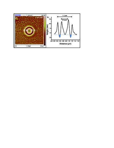
CMS 400 forms the double ring with some asymmetry and the outer diameter is of the order of 5 m. Along with the ring formation, a spread of the material in the vicinity of the modified region which is identified as a corona effect is seen on these films. Whereas CMS 600 forms highly irregular shaped features, often it was found difficult to modify the CMS 600 surface. CMS 500 surface consistently gives a highly symmetric double ring structure with least spread to the surroundings. No corona effect is observed for CMS 500 and 600 films. Figure 2 shows a cross sectional profile across the diameter of one such ring produced on CMS 500 surface. The double ring formation is highly symmetrical as seen in Fig 2(a). The diameter of the outer ring as measured from line profile shown in Fig. 2(b), is 1.1 m and 0.6 m for the inner ring. The height of the rim of the ring is 12 nm. The AFM image and the shaded region in the line profile prove that the material from the region between the two rings is being ablated during the application of bias. Even surface in the vicinity of ring is modified. This represents the phenomena of stress induced by the biased AFM tip on the surface and electrical break down of the film, under intense electric fields. To evaluate whether the material has undergone electrical breakdown, we have done the KPFM analysis of one such modified region of CMS 400 film as shown in figure 4b along with the topography of the film in Fig. 3(a). In KPFM, the contact potential difference (CPD) betweem the metal tip and sample surface is estimated based on Fermi level equilibrium model.27 This is the amount of voltage required to nullify the electrostatic force generated between two materials due to their work function difference. The lower CPD in the modified region as seen in Fig. 3(b) is a clear indication that negative charge is induced in the modified region and its origin is the dielectric breakdown of CMS films.28
The pattern formed is a clear signature of dielectric breakdown. As crystallinity of films improve with TA, the threshold for electrical breakdown also increases due to reduction in number of traps.29 This agrees well with the trend observed in Fig. 1 in comparison with X-ray diffraction data shown in Fig. S1. Hence CMS 600 film of high crystalline quality is unlikely to undergo easy electrical breakdown where as CMS 400 can be ablated easily and the material spread to the surroundings. However, the formation of symmetric ring features on CMS films is very distinct and intriguing. To understand any contribution from the magnetic nature of these films and interaction of the ablated material with the magnetic field generated by the conducting tip, the ring and their surroundings formed on CMS 400 thin film were mapped for their magnetic nature by magnetic force microscopy (MFM). Energy dispersive spectroscopy (EDS) was also done for elemental analysis of various regions of the ring. Both these results unequivocally showed that the distributed material is magnetic in nature and mostly rich in Co. Figure 4 summarizes the results of MFM and EDS analysis of the ring and its corona. The AFM topographic image and the MFM image at a lift height of 30 nm, collected from the same area are displayed in Fig. 4(a) and 4(b) respectively. The MFM images have a phase variation different from the rest of the film explaining the magnetic nature of the dispersed material. Clearly, the intermittent out of phase variation of outer rim and inner rim of the double ring, pointed by arrow marks in MFM image i.e., Fig. 4(b) explains the non magnetic behavior. This negative phase variation could be due to the local anodic oxide formation along the rim of the CMS rings.
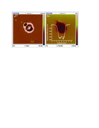
Figure 4d shows the energy dispersive spectrum of different elements from the CMS film. The inset shows the variation in atomic % of Co for different regions of the SEM image in Fig. 4(c). Region 1 corresponds to the ablated portion of the ring, region 2 is the corona portion of the ring and region 3 is the unmodified substrate region. High atomic % of Co in the vicinity of the ablated region compared to rest of the film explains the enhanced magnetic contrast of MFM image in figure 5b. This clearly says that the pattern formation and the spread of the material on CMS films are due to the interaction of Oersted’s field with the material itself. This is a distinct phenomenon compared to general corona effect observed during LAO of semiconductors and metals. The electric field intensity (E) at the edge of the AFM tip for a bias of -12 volts is of the order V/cm.30 The corresponding current density (J) can be estimated by field emission phenomena based on Fowler-Nordhiem theory (F-N theory).31
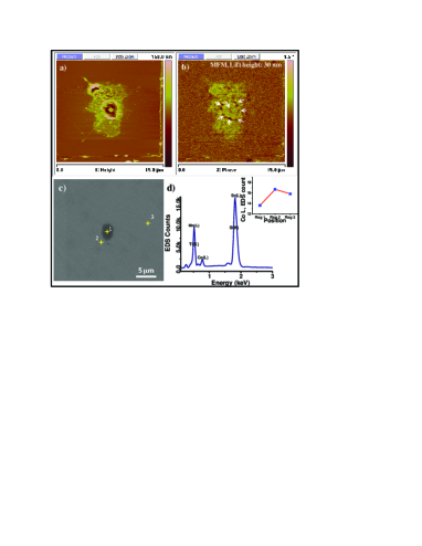
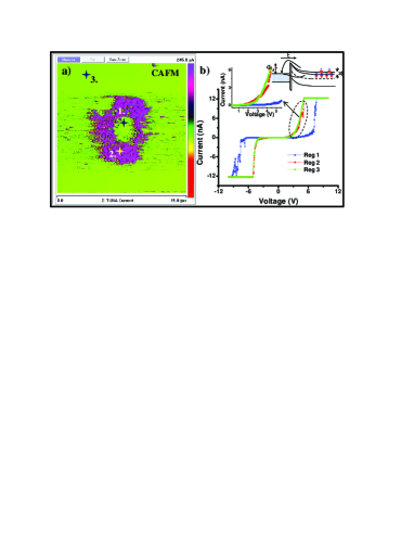
Figure 5 shows the conductivity mapping of the double ring on CMS 400 film at tip voltage of 3 V, along with current-voltage characteristics from different regions captured by point and shoot I-V spectroscopy mode. The contrast of the current map in Fig. 5(a) reveals that the conductivity of corona region (Region 2) is more compared to that of the bare region (Region 3) and the rim region (Region 1). Figure 5(b) shows the I-V characteristics captured from these three different regions of the ring structure along with an inset showing the section of I-V characteristics and the schematic of electron transport. From the I-V curves it is clear that the conductance of the rim region (Region 1) is less than that of the Region 2 and 3 which are taken from the corona and bare CMS respectively, proving that it is mostly oxide. The behavior of I-V characteristics are typical of a schottky junction. For such junctions, current in forward bias is dominated by majority charge carriers. Modified I-V characteristics for schottky junction in the present case can be expressed as;
| (1) |
where IS is the saturation current, B is Schottky barrier height, P is the non equilibrium spin polarization in the n region, v is applied voltage, A is area, and A⋆ is Richardson’s constant. The current map in Fig. 5(a) agrees well with the I-V characteristics below 3 V from Region 2 and Region 3 as shown in the inset of Fig. 5(b). Difference in the steepness of I-V characteristics in the forward bias from both regions above 3 V gives an indication that the current from Region 3 has a contribution not only from charge drift but also from spin, making it behave like a Spin diode.34 The transport characteristics in forward bias is similar to the current injection in spin diode, where the I-V characteristics are expressed as35 :
| (2) |
where Pp is equilibrium spin polarization in the p region. When unpolarized current is passed across a ferromagnetic semiconductor, the current becomes spin-polarized.36 ; 37 Electrons which are spin polarized in this material could show a strong interaction with the applied current. Transverse spin current has been recently demonstrated experimentally in GaAs thin films,38 and in AlGaAs quantum wells.39 The steeper I-V characteristics for bare region compared to modified region indicates the spin contribution in the transport and loss of half metallicity of the modified region due to electrical breakdown.
Double ring structures were formed on Co2MnSi films via electric breakdown, using conducting AFM tip. These rings were analyzed using magnetic force microscopy and energy dispersive spectroscopy. MFM of the rings suggest that the dispersed material forming a corona is magnetic and EDS confirmed that the material is rich in Co. The ring formation is explained in terms of the interaction of ablated material with the magnetic field produced by the conducting AFM tip. Local I-V spectroscopy using Co tip on the ring and its surrounding regions suggest that the system forms a schottky diode when in contact with the tip. The I-V characterization from bare region indicate that the transport is influenced by the spin polarization nature of conduction electrons in CMS. Further experiments of I-V characterization at different temperatures and in the presence of magnetic field will confirm the observation of spin transport of the system.
VKT thanks Dr. Sukhwir Singh for his support and cooperation in accessing the AFM facility, Mr. K. N. Sood for getting SEM data and Dr. S. T. Lakshmi Kumar for his valuable comments about the work. H.P. acknowledges financial support from Indian Institute of Technology (IIT) Kanpur and the Council for Scientific and Industrial Research (CSIR), Government of India. R.C.B. acknowledges the J. C. Bose fellowship of Department of Science and Technology. The Work carried out at IIT Kanpur has been supported by the Department of Information Technology.
References
- (1) J. A. Dagata, J. Schneir, H. H. Harary, C. J. Evans, M. T. Postek, J. Bennett, Appl. Phys. Lett. 56 (1990) 2001.
- (2) J. A. Dagata, T. Inoue, J. Itoh, K. Matsumoto, H. Yokoyama, J. Appl. Phys. 84 (1998) 6891.
- (3) E. S. Snow, D. Park, P. M. Campbell, Appl. Phys. Lett. 69 (1996) 269.
- (4) L. A. Nagahara, T. Thundat, S. M. Lindsay, Appl. Phys. Lett. 57 (1990) 270.
- (5) J. S. Hwang, Z. S. Hu, T. Y. Lu, L. W. Chen, S. W. Chen, T. Y. Lin, C. L. Hsiao, K. H. Chen, L. C. Chen, Nanotechnology 17 (2006) 3299.
- (6) J. S. Hwang, Z. Y. You, S. Y. Lin, Z. S. Hu, C. T. Wu, C. W. Chen, Appl. Phys. Lett. 86 (2005) 161901.
- (7) M. Rolandi, C. F. Quate, H. Dai, Adv. Mater. 14 (2002) 191.
- (8) C. Huh, S. J. Park, J. Vac. Sci. Technol. B 18 (2000) 55.
- (9) D. Wang, L. Tsau, K. L. Wang, P. Chow Appl. Phys. Lett. 67 (1995) 1295.
- (10) H. Sugimura, T. Uchida, N. Kitamura, H. Masuhara, J. Phys. Chem. 98 (1994) 4352.
- (11) M. Tello, R. Garcia, J. A. Mart n-Gago, N. F. Mart nez, M. S. Mart n- Gonz le, L. Aballe, A. Baranov, L. Gregoratti, Adv. Mater. 17 (2005) 1480.
- (12) H. Kuramochi, F. Perez-Murano, J. Dagata, H. Yokoyama, Nanotechnology 15 (2004) 297.
- (13) T.-H. Fang, Microelectron. J. 35 (2004) 701.
- (14) X. N. Xie, H. J. Chung, Z. J. Liu, S. W. Yang, C. H. Sow, A. T. S Wee, Adv. Mater. 19 (2007) 2618.
- (15) G. Mori, M. Lazzarino, D. Ercolani, G. Biasiol, L. Sorba, S. Heun, A. Locatelli, J. Appl. Phys. 98 (2005) 114303.
- (16) L. Zhang, Y. Mitani, Appl. Phys. Lett. 88 (2006) 032906.
- (17) R. Waser, M. Aono, Nature Materials 6 (2007) 833.
- (18) M. J. Lee, C. B. Lee, D. lee, S. R. Lee, M. Chang, J. H. Hur, Y. B. Kim, C. J. Kim, D. H. Seo, S. Seo, U. I. Chung, I. Chung, K. Kim, Nature Materials 10 (2011) 625.
- (19) S. J. Gamble, M. H. Burkhardt, A. Kashuba, R. Allenspach , S. S. Parkin, H.C. Siegmann, J. Stohr, Phys. Rev. Lett 102 (2009) 217201.
- (20) P. J. Brown, K. U. Neumann, P. J. Webster, K. R. A. Ziebeck, J. Phys.: Cond. Matt. 12 (2000) 1827.
- (21) P. J. Webster, J. Physics and Chemistry of Solids 32 (1971)1221.
- (22) S. Ishida, T. Masaki, S. Fujii, S. Asano, Physica B: Condensed Matter 239 (1997) 163.
- (23) L. Ritchie, G. Xiao, Y. Ji, T. Y. Chen, C. L. Chien, M. Zhang, J. Chen, Z. Liu, G. Wu, X. X. Zhang, Phys. Rev. B 68 (2003) 104430.
- (24) S. J. Hashemifar, P. Kratzer, M. Scheffler, Phys. Rev. Lett. 94 (2005) 096402.
- (25) H. Pandey, P. C. Joshi, R. P. Pant, R. Prasad, S. Auluck, R. C. Budhani, J. Appl. Phys. 111 (2012) 023912.
- (26) See supplementary material for structural and magnetic characterization.
- (27) I. D.Baikie, P. J. Estrup, Rev. Sci. Instrum. 69 (1998) 3902.
- (28) M. Porti, M. Nafria, M. C. Blum, X. Aymerich, S. Sadewasser, Appl. Phys. Lett. 81 (2002) 3615.
- (29) C. L. Sun, S.Y. Chen, S. B. Chen, A. Chin, Appl. Phys. Lett. 80 (2002) 1984.
- (30) J. J. Ahn, K. S. Moon, S. M. Koo, Nanoscale Res. Lett. 6 (2011) 550.
- (31) R. H. Fowler, L. Nordheim, Proc. R. Soc. London, Ser. A, 119 (1928) 173.
- (32) K. E. Aidala1, A. Hanbicki, Appl. Phys. Lett. 80 (2002) 1240.
- (33) I. Zutic, J. Fabian, S. D. Sarma, Rev. Mod. Phys. 76 (2004) 323.
- (34) J. S. Moodera, X. Hao, G. A. Gibson, R. Meservey, Phys. Rev. Lett. 61 (1988) 637.
- (35) J. Fabian, I. Zutic, S. D. Sarma, Phys. Rev. B 66 (2002) 165301.
- (36) Y. K. Kato, R. C. Myers, A. C. Gossard, D. D. Awschalom, Science 306 (2004) 1910.
- (37) V. Sih, R. C. Myers, Y. K. Kato, W. H. Lau, A. C. Gossard, D. D. Awschalom, Nat. Phys. 1 (2005) 31.