Time-resolved measurement of the tunnel magneto-Seebeck effect in a single magnetic tunnel junction
Abstract
Recently, several groups have reported spin-dependent thermoelectric effects in magnetic tunnel junctions. In this paper, we present a setup for time-resolved measurements of thermovoltages and thermocurrents of a single micro- to nanometer-scaled tunnel junction. An electrically modulated diode laser is used to create a temperature gradient across the tunnel junction layer stack. This laser modulation technique enables the recording of time-dependent thermovoltage signals with a temporal resolution only limited by the preamplifier for the thermovoltage. So far, time-dependent thermovoltage could not be interpreted. Now, with the setup presented in this paper, it is possible to distinguish different Seebeck voltage contributions to the overall measured voltage signal in the time regime. A model circuit is developed that explains those voltage contributions on different sample types. Further, it will be shown that a voltage signal arising from the magnetic tunnel junction can only be observed when the laser spot is directly centered on top of the magnetic tunnel junction, which allows a lateral separation of the effects.
pacs:
85.30.Mn, 85.80.-b, 85.75.-d, 85.75.Dd, 75.76.+j, 79.10.N-, 73.50.Jt,I Introduction
In recent years, the research field “spin caloritronics” has attracted considerable attention in the magnetism and spintronics communitiesBauer, MacDonald, and Maekawa (2010); Bauer, Saitoh, and van Wees (2012). New spin-dependent thermoelectric effects have been discovered in ferromagnetic metalsUchida et al. (2008), insulatorsUchida et al. (2010) and semiconductorsJaworski et al. (2010). Triggered by the experiments of Gravier et al.Gravier et al. (2006) and Shi et al.Shi et al. (1993) on giant magneto resistance (GMR) multilayers, and by theoretical predictions of large magnetothermoelectric effects in magnetic tunnel junctionsCzerner, Bachmann, and Heiliger (2011), several groups reported observations of a tunnel magneto-Seebeck effect (TMS) in magnetic tunnel junctions (MTJs) with MgO-Liebing et al. (2011); Walter et al. (2011) and alumina-barriersLin et al. (2012). A closely related effect is thermal spin injection into silicon through Seebeck spin tunnelingLe Breton et al. (2011). In non-local spin valves, thermally driven spin injection was discoveredSlachter et al. (2010) and Peltier and Seebeck effects were studiedBakker et al. (2010). The number of these new effects, combined with the proposed thermal spin-transfer torque Jia, Xia, and Bauer (2011); Leutenantsmeyer et al. (2013) might enable the fabrication of thermally driven Magnetoresistive Random Access Memory (MRAM) and other spintronic devices.
Some of the effects are vividly discussed in the community.Kikkawa et al. (2013); Geprägs et al. (2012); Huang et al. (2012); Meier et al. (2013); Qu et al. (2013); Avery, Pufall, and Zink (2012); Lu et al. (2013) In contrast, the experiments on CoFeB/MgO-based MTJs with high tunnel magnetoresistance (TMR) ratios, in which either a laserWalter et al. (2011) or resistive heatingLiebing et al. (2011) is used to generate the temperature gradients, show comparable results. These are of the same magnitude as predicted by ab initio calculations.Czerner, Bachmann, and Heiliger (2011); Walter et al. (2011) For MTJs with alumina-barrier, larger Seebeck voltages as compared to MgO-barriers at comparable temperature gradients are found. However, there are a few variations between the different experiments: First, the sign of the Seebeck voltage remains unclear, which could also vary depending on temperature and Co-Fe-composition.Heiliger, Franz, and Czerner (2013) Further, it was reported by Ref. Lin et al., 2012 that no magnetic effect is observed in the thermocurrent obtained with alumina-barriers and that Seebeck voltages could be observed when heating the electrical leads a distance of the order of millimeters away from the MTJ.
In the following, we will address these issues and show results for the Seebeck voltage as well as for the thermocurrent and the determination of the voltage sign with a lock-in technique in section IV. A model circuit is developed in section V to interpret the time-dependent signals. In section VI heating-position dependent measurements are presented, which reveal that the Seebeck voltage is generated locally at the MTJ in this geometry.
II Description of the experimental setup
The setup used in this work is based on the experiments performed by Gravier et al.Gravier et al. (2004) on metallic nanowires. We adapted the electrical and optical techniques to the requirements for measuring small thermovoltages across a micrometer-sized single MTJ.
To heat the MTJ from the top and to create a temperature gradient across the layer stack, a laser diode (Toptica ibeam-smart-640-s) is focused down to a beamwaist of – using a microscope objective (Mitutoyo M Plan Apo 10x). The central laser wavelength is 637 nm. An exact positioning of the laser spot onto the MTJ is crucial for obtaining reliable voltage measurements. Thus, the position of the laser spot can be controlled using a confocal microscope as depicted in FIG. 1 (a). With a set of different electromagnets, the sample can be studied in magnetic fields in-plane and perpendicular to plane.
The thermovoltage is detected with a lock-in amplifier. In our earlier publicationWalter et al. (2011), a mechanical chopper was used to modulate the laser heating at , however it was found that the beamwaist of the unfocussed laser in combination with the mechanical chopping decreases the time-resolution of the thermovoltage detected by the oscilloscope. As a consequence, a waveform generator (Agilent 33500B) has been implemented to modulate the laser diode power with a square wave of . As can be seen from FIG. 1 (a), a fast photodiode (EOT ET-2030, rise time of ) is integrated in the confocal microscope part of the setup to check the square-wave form of the light intensity. With this optical setup a rise and fall time of of the light intensity can be achieved. This is faster than the rise time of the preamplifier used for high impedance MTJs. Thus, the time-resolution of the measured voltage signal of the MTJs is only limited by the electronic equipment,
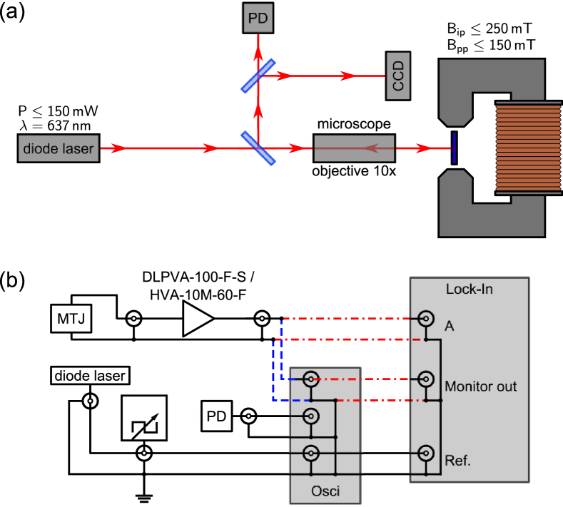
which is shown in FIG. 1 (b): The MTJ is connected to a precision voltage preamplifier via shielded cables (total length 1.6 m). Depending on the MTJ resistance either a high impedance amplifier (femto DLPVA-100-F-S) with a rise time of or a faster amplifier for low impedance sources (HVA-10M-60-F) with a rise time of can be used. The signal preamplified by to is then fed either to the oscilloscope directly (blue dashed line in FIG.1 (b)) or to the lock-in amplifier (red dash-dotted line in FIG.1 (b)). In the latter case, the time-dependent voltage signals are recorded by the oscilloscope which then is connected to the monitor out of the lock-in amplifier. A Stanford Research Systems SR830 lock-in amplifier and a Philips PM3382 oscilloscope are used. All electrical components are triggered by the waveform generator and carefully grounded to minimize noise coupling into the measurement circuit. The noise level of the setup is within a range of to , which is of the same order as Johnson-Nyquist-noise of the MTJ’s resistance at room temperature. The low noise level enables observing small voltage changes on the order of nanovolts at low laser intensities, as shown in FIG. 2.
For a thermocurrent measurement, the MTJ is connected without preamplifier to the lock-in amplifier set to current detection.
II.1 Determination of temperatures
Since the CoFeB and MgO layers of only a few nanometer thickness are buried under several layers of electrical leads, it is very difficult to reliably measure the temperature difference across them. Putting thermocouples to the electrical leads of the MTJ can only give a rough estimate of the temperature distribution.
| Material | |||
|---|---|---|---|
| Au | 19.32 | 128 | 320.0 / 70111Ref. Zink et al., 2005 – 170222Ref. Zhang et al.,2006 |
| Cr | 7.15 | 449 | 94.0 |
| Ru | 12.37 | 238 | 117.0 |
| Ta | 16.65 | 140 | 57.0 |
| Permalloy | 8.7 | 460 | 19.0 |
| IrMn | 10.18 | 69.7 | 6.0 |
| Co-Fe-B | 8.22 | 440 | 86.7 |
| MgO | 3.58 | 935 | 48.0 / 4.0333Ref. Lee, Cahill, and Allen,1995 |
| SiO2 | 2.20 | 1052 | 1.4 |
| Si | 2.33 | 700 | 150.0 |
| SiN | 3.11 | 700 | 35.9 |
Consequently, the heat conduction equation is, therefore, numerically solved using COMSOL MultiphysicsCOM to determine the temperatures of the MTJ layers. The results have to be regarded as estimates, since interface heat resistances are not taken into account and bulk values of thermal conductivities, densities and heat capacities are used for the metals layers. These material parameters are taken from literature shown in TABLE 1 for the MTJ materials. The table shows that the thermal conductivity of an Au thin film is lower by at least a factor of 2. In addition, we used the experimentally observed thin film value for the MgO layer, because here the thermal conductivity changes by an order of magnitude. This improves the reliability of our simulations.Lee, Cahill, and Allen (1995); Walter et al. (2011) Further details on the simulations can be found in earlier publications.Walter et al. (2011); Leutenantsmeyer et al. (2013) The temperature difference across the MgO layer resulting from the simulations is used in section IV.1 in combination with the measured voltage to calculate the Seebeck coefficients.
III Sample preparation
The MTJs are prepared on two types of substrates: MgO and oxidized p-type silicon (Si) ( , resistivity of ) by sputter deposition in a Leybold Vakuum GmbH CLAB 600. The film system on MgO consists of bottom contact Ta 5/Ru 30/Ta 10/Ru 5; pinned layer MnIr 15/CoFeB 3; tunnel barrier MgO 1.5; free layer CoFeB 3/NiFe 6; top contact Ta 3/Ru 3/Ta 3/Au 15 (thickness are given in nm). In case of Si/ substrates the pinned layer is slightly changed to MnIr 12/CoFe 3/Ru 0.9/CoFeB 3. Elliptical MTJs with a size of are produced by electron beam lithography and subsequent ion beam etching. Afterwards, 100 nm of SiN are sputter deposited next to the MTJs as insulator. An Au bond pad is placed adjacent to the MTJs in an additional sputtering and patterning process for connecting the 15 nm Au top contact to the measurement electronics. This allows free optical access to the MTJ.
IV Experiments on Magnesium oxide and Silicon substrates
IV.1 TMR and TMS measurements
Thermoelectric effects can be derived theoretically from thermodynamic principles. For the case of an MTJ, the thermoelectric coefficients dependent on the tunneling probability can be expressed by equations based on the Landauer formula.Callen (1960); Büttiker et al. (1985); Sivan and Imry (1986); Czerner, Bachmann, and Heiliger (2011); Lin et al. (2012) In this way, the influence of spin transport on the Seebeck voltage of an MTJ can be described. To clarify the interconnection between the different transport coefficients and sign conventions, we first derive the Seebeck voltage, Seebeck current, TMS and TMR from the thermodynamic kinetic equations and the moments of the transport integral.
The charge transport through the barrier of the MTJ is given as
| (1) |
where is the electric conductance and is the Seebeck coefficient. According to eq. 1, a current is either generated by an external voltage or by a temperature gradient . In a Seebeck current measurement no external voltage is applied to the MTJ () whereas in a perfect voltage measurement no current is transported in the circuit (), which yields
| (2) |
for the measured current and voltage, respectively. The coefficients can be rewritten asOuyang and Guo (2009); Czerner, Bachmann, and Heiliger (2011)
| (3) |
using the moments
| (4) |
dependent on , the Fermi occupation function at a given energy , electrochemical potential and temperature and on the energy-dependent transmission probability that is different for the parallel (P) and antiparallel (AP) orientation of the bottom and top layer’s magnetization, which leads to different moments for both statesCzerner, Bachmann, and Heiliger (2011); Walter et al. (2011). Thus, the TMS is calculated analogous to the TMR:
| (5) |
The MTJs on Si/ and MgO were prepared to investigate the influence of the substrate material on the TMR and TMS measurements. FIG. 2 shows field dependent resistance and Seebeck voltage curves of elliptical MTJs with an area of 19 prepared on Si/ and MgO, respectively.
In case of the Si/ substrate, the resistance of the MTJ switches between in the antiparallel and in the parallel orientation of the ferromagnetic layers, which yields a TMR ratio of . The Seebeck voltage, generated by laser heating with a power of 10 mW, changes from in the antiparallel to in the parallel state resulting in a TMS ratio of . The Seebeck voltage detected by the lock-in amplifier is positive as shown in FIG. 4 (a). This means that the electrons are accumulated at the cold electrode, which results in a negative Seebeck coefficient (eq. (2)).
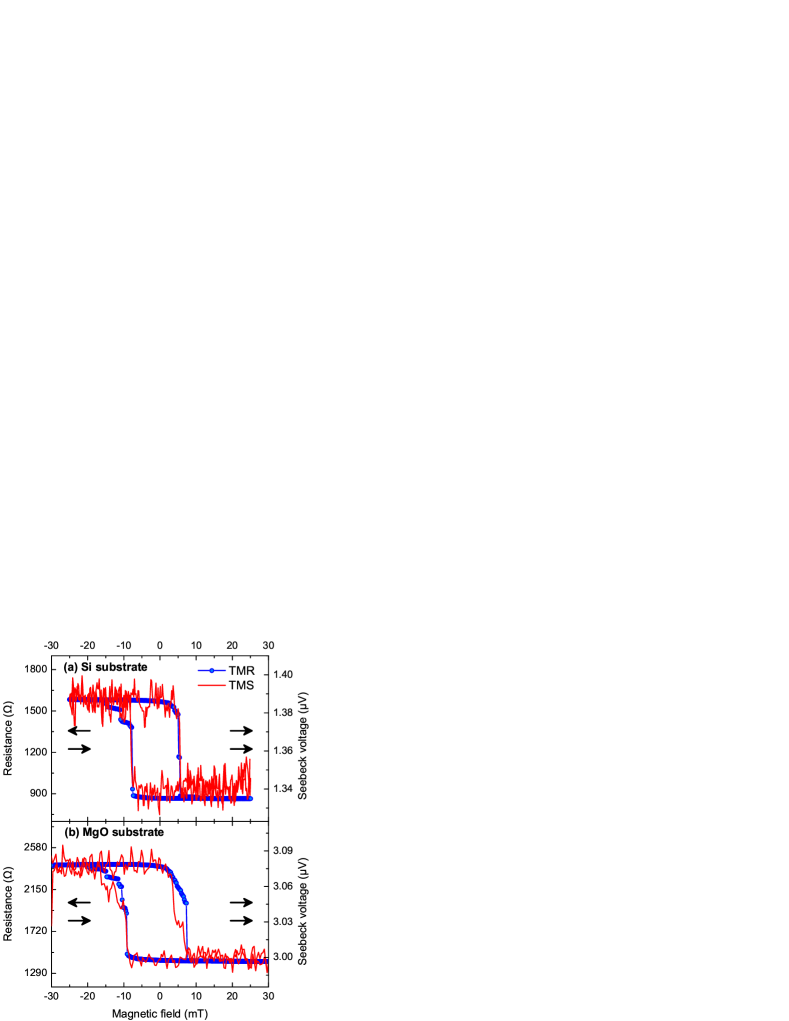
The MTJ on MgO exhibits a larger resistance than the MTJ on Si/ substrate. The resistance varies between in the antiparallel and in the parallel state. A TMR ratio of is obtained. The corresponding Seebeck voltage, induced by laser heating with 15 mW laser power, switches at the same magnetic fields between and gaining a TMS ratio of . As for the MTJ on Si/ substrate, the Seebeck voltage is again positive (FIG. 4 (b)).
In TABLE 2 the parameters of the TMR and TMS are shown. The small differences are within the normal deviations between different MTJs and can also be due to different growth conditions on the two substrates. As a consequence, no evidence for influence of parasitic Seebeck voltages arising from different substrates on the TMS measurements is found.
The Seebeck coefficients in TABLE 2 are calculated from the above mentioned simulated temperature gradient across the barrier and the thermovoltage generated inside the MTJ. This thermovoltage consists of a spin-dependent component from the ferromagnetic electrodes and a spin-independent background from the other layers in the MTJ. A possible solution to estimate this spin-independent background is given in Ref.Liebing et al., 2012: The MTJ is forced to a dielectric breakdown after the TMS measurement is performed and the remaining, spin-independent background thermovoltage is determined. The background thermovoltage is approximately up to , such that after subtraction, the resulting TMS ratios are around 20 % for the data presented in this paper. However, the morphology of the layers changes due to the voltage stress applied to the MTJ, e.g. the CoFeB can change from an amorphous to a crystalline structure and the interfaces between the thin films can be destroyedThomas et al. (2008). Therefore, this method allows only an estimation for the background thermovoltages arising from other sources of the layer stack of the tunnel junction that do not contribute to the TMS itself.
| substrate | TMR | ||
|---|---|---|---|
| Si | 864 | 1583 | 83 % |
| MgO | 1411 | 2400 | 70 % |
| substrate | 444 is used for Si/ substrate and for MgO substrate. | 11footnotemark: 1 | TMS | ||
| Si | 1.34 | 1.39 | -223 | -232 | 3.7 % |
| MgO | 3.00 | 3.08 | -750 | -770 | 2.6 % |
IV.2 Thermocurrent measurements
In an open circuit, the Seebeck effect creates a voltage in an MTJ experiencing a temperature gradient, whereas in a closed circuit geometry, it can drive a Seebeck current. FIG. 3 shows the magnetization dependence of the Seebeck voltage and Seebeck current induced by laser heating with a power of 150 mW for an MTJ on MgO with an area of and a resistance of in the antiparallel and in the parallel state. Note that the laser power is considerably larger than in the first example (FIG. 2). The voltage varies between in the antiparallel and in the parallel state, whereas the current behaves inversely such that it reaches and , respectively. This yields a TMS ratio of and a current effect-ratio of .
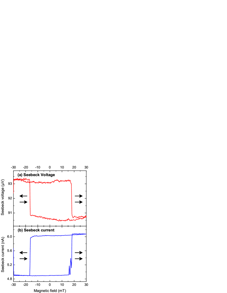
Since the moments in eq. (4), which depend on the magnetization dependent transmission , occur in the conductance as well as in the Seebeck coefficient (eq. (3)), both, the voltage and the current should exhibit a magnetic field dependent variation, as suggested by eq. (2). This prediction is confirmed by our experimental results. The difference in the effect amplitudes is explained by the fact that, as it can be seen in eq. (2), the voltage only depends on the Seebeck coefficient , whereas the current is additionally dependent on the electrical conductance , which is strongly dependent on the magnetization alignment due to the high TMR ratio.
Seebeck currents were also investigated by Lin et al.Lin et al. (2012), but in contrast to our measurements they do not detect a dependency of the current on the magnetic field which they explain by the different mechanisms causing TMS in alumina-based MTJs. On Co-Fe-B/MgO MTJs, Liebing et al. demonstrated magnetic switching in Seebeck current measurements very recently.Liebing et al.
IV.3 Time-dependent thermovoltage signals
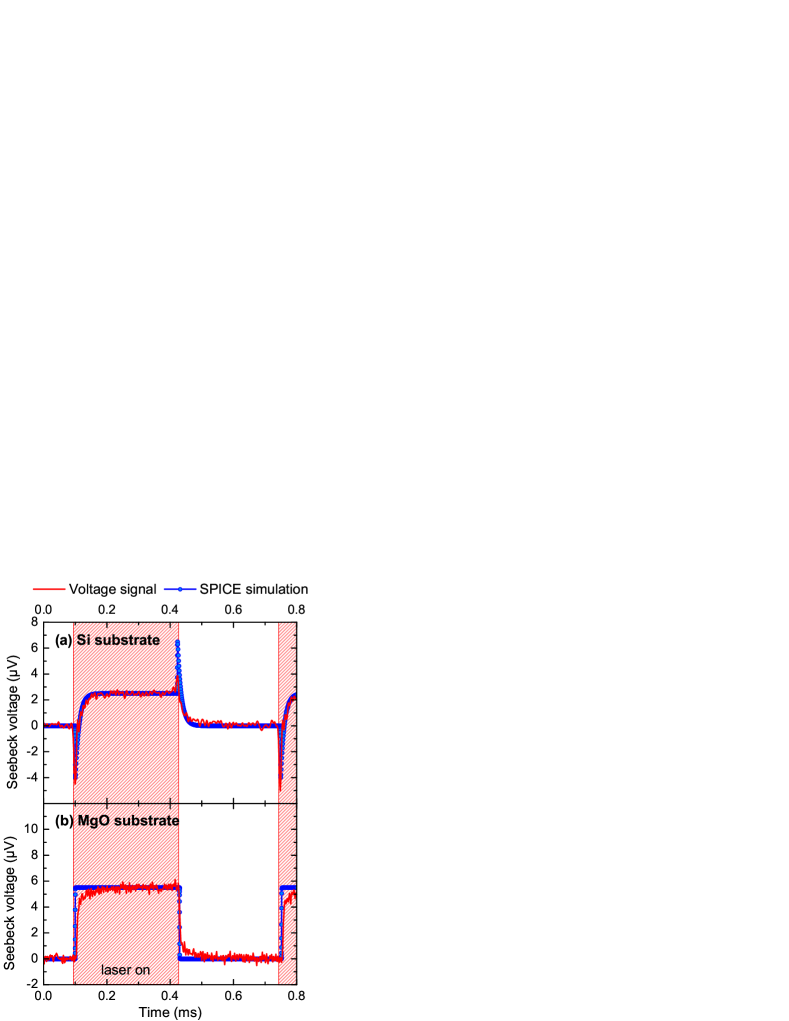
To gain a deeper understanding of the processes leading to the TMS signal measured by the lock-in amplifier, a closer investigation of the time-dependent voltage signal is essential. It is assumed that the temperature gradient rapidly increases and decreases upon laser on/off, which is justified by temperature simulations yielding a time of to reach equilibrium. Thus, a nearly rectangular time-dependent voltage signal is expected corresponding to the laser modulation.
In FIG. 4, the time-dependent voltage signals of MTJs on Si/ and MgO are depicted. The traces for both substrate materials clearly reveal voltage plateaus with a small rise and fall-time when the laser is turned on and off. Whereas on MgO the rectangular shape is clearly visible, unexpected negative and positive voltage peaks can be additionally observed at the start and end of the heating period on Si/. The position and shape of these voltage peaks suggest an electrical capacitance as their origin. The source can be further restricted to the substrate as the additional voltage only occurs in samples with p-doped Si substrate which is capacitively coupled to the bottom electrode by the dielectric.
V Development of a model circuit
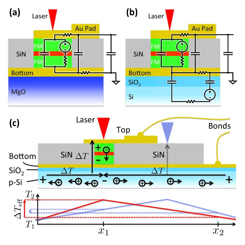
Uncovering the processes responsible for the strikingly different temporal voltage traces measured on MgO and Si/ substrates can be achieved by describing the sample structure as a model circuit. FIG. 5 sketches how the relevant parts inside the sample can be converted into an equivalent circuit consisting of three major units.
| comp. | how to calculate | value |
|---|---|---|
| extracted from TMR data | ||
| fit to data (value of plateau) | ||
| fit to data | ||
| parallel plate capacitor: MgO thickness, MTJ area | ||
| geometric dimensions of Au pad and resistivity of Au | ||
| parallel plate capacitor: SiN thickness, area of bond pad | ||
| given by manufacturer | ||
| effective parallel plate capacitor with dielectric | ||
| geometric dimension of Si substrate, conducting channel is created between MTJ and bond wire contact to bottom electrode | ||
| geometric dimensions of conducting channel inside the bottom electrode between MTJ an bond wire contact |
The first part is the MTJ simplified as a voltage source simulating the Seebeck voltage generated by the temperature gradient across the barrier, a resistor representing the dielectric barrier and a capacitor describing the capacitance built up by the two ferromagnetic layers (FM) separated by the MgO.
The second unit contains the electrodes and wiring including the resistance of the bottom electrode and of the top contact, mainly the gold bond pad . Furthermore a capacitance is build up by the gold pad and the bottom electrode separated by the insulator surrounding the MTJs. It is supplemented by the cable capacitance of the coaxial cables connecting the sample to the electronic equipment.
The third major component is the substrate. In case of MgO samples, the substrate is insulating and therefore has not to be taken into account when constructing a model circuit (FIG. 5 (a)). When Si samples are depicted, the substrate is a p-type semiconductor that creates a Seebeck voltage when heated (FIG. 5 (b)) that capacitively couples to the bottom electrode through the capping. The temperature gradient inside the substrate arises when the MTJ is heated. Not only the upper side of the MTJ is heated when irradiated by the laser, but also the lower part near the substrate experiences an elevated temperature due to heat conduction through the layer stack. Thus, the temperature inside the substrate underneath the MTJ is higher than at the edges of the sample. The resulting temperature gradient creates a Seebeck voltage in the p-Si substrate as sketched in FIG. 5 (c). This effect is included in the model circuit by adding a voltage source and two capacitances , one underneath the MTJ and another at the point where the bottom electrode is connected to the gold bond wire, as these two points confine the segment where a capacitively coupled voltage can be detected (FIG. 5 (b)).
The size of all capacitances can be calculated from the model of a parallel plate capacitor except the cable capacitance that is given by the manufacturer. The sum of the resistors , and connected in series has to match the measured TMR whilst the value of and can be deduced from the geometric dimensions of the conduction channel constituting between the MTJ and the contact point of the bottom electrode to the gold bond wire.
FIG. 4 shows a good agreement of SPICE simulations of the model circuit with the measured data. Our model of a Seebeck voltage created in the silicon substrate that cannot occur inside the MgO substrate explains the effects observed in the experiment. The absolute values of the voltages and have to be deduced. All other components are calculated and summarized in TABLE 3. Considering that the relation of the amplitude detected by the oscilloscope and the voltage output of the lock-in amplifier is given by for a square wave signal, the measurements of FIG. 4 agree very well with those of FIG. 2. Based on these results, we are able to assign the different measured voltages to a Seebeck effect inside the MTJ on the one hand and a Seebeck effect inside the substrate material on the other hand.
VI Position-dependent measurements
The tunnel magneto-Seebeck effect should arise from Seebeck voltages generated by a temperature gradient across the MgO layer sandwiched between two ferromagnets. From the underlying geometry of the MTJ sketched in FIG. 5 (c) we conclude that moving the laser spot away from the junction on the gold bond pad should already decrease this temperature gradient and hence the observed Seebeck voltage. Furthermore, lateral temperature gradients created by the laser spot on the gold bond pad should cancel out because of the lateral radial symmetry of the heating.
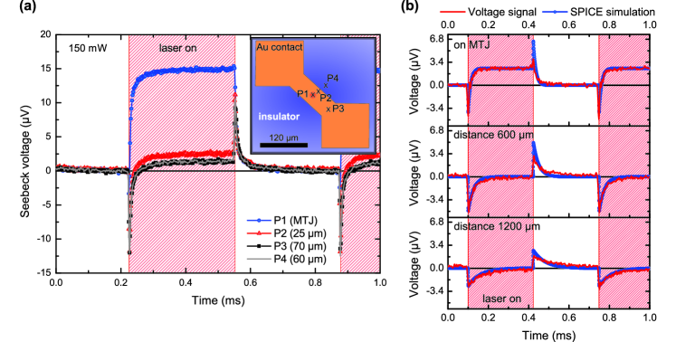
We performed several position-dependent measurements in the vicinity of the gold bond pad of the junction, and also with the laser spot moved more than away from the MTJ. The inset of FIG. 6 (a) shows the geometry of the bond pad with the MTJ located at position P1. The area heated by the laser is sketched as a red circle. Its diameter is according to simulationsCOM only slightly larger than the laser spot (). TMS measurements were taken with the laser positioned at P1 – P4. The corresponding time-dependent voltage signals are shown in FIG. 6 (a). It can be seen that a square-wave-like Seebeck voltage that is attributed to the MTJ, as discussed in Secs. IV–V, occurs only if the laser spot is centered directly onto the MTJ at P1. Only at this position the TMS effect is observed. At position P2, adjacent to the MTJ, the Seebeck voltage of the MTJ is already strongly reduced. Only the voltage peaks attributed to voltages generated in the Si substrate occur at all four positions. Time-dependent voltage signals were recorded also for large distances, which are shown in FIG. 6 (b): It is observed that the time constant of the exponential decay of the voltage peaks increases with distance. The plotted simulated curves describe the signals reasonably well. In the model, the MTJ voltage is set to zero for non-zero distances between the laser and the MTJ and the voltage peaks can be reproduced by adjusting the resistance of the substrate and by lowering the generated voltage (reduced effective temperature gradient, FIG. 5 (c)) according to the increased distance.
These findings support the attribution of the voltage peaks to parasitic voltages of the Si/ substrate. Further, they show that the setup enables us to discriminate voltages locally generated in a single MTJ.
VII Conclusion
In summary, we have presented an experimental setup that allows the reliable measurement of thermomagnetoelectric effects in a single tunnel junction with nanovolt resolution at a temporal resolution of a few microseconds. MTJs grown on oxidized Si and MgO substrates have been tested and show comparable Seebeck voltages and currents. We find a magnetic effect also in the Seebeck current measurements. Further, with the improved temporal resolution, the voltage signals of the MTJs can be interpreted with the help of a model circuit. On oxidized Si substrates an additional voltage generated in the substrate can be identified. However, no evidence is found that this voltage influences the TMS measurements carried out with a lock-in amplifier. Distance dependent measurements reveal that the detected Seebeck voltage originates only from the MTJ layer stack. When the laser is moved away from the MTJ, only the Seebeck voltage signal of the substrate can be found.
Acknowledgements.
M.M., A.T., and G.R. are supported by the DFG through SPP 1538 SpinCaT (MU1780/8-1, RE1052/24-1). V.D. and A.T. are supported by the Ministry of Innovation, Science and Research (MIWF) of North Rhine-Westphalia with an independent researcher grant.References
- Bauer, MacDonald, and Maekawa (2010) G. E. Bauer, A. H. MacDonald, and S. Maekawa, Solid State Commun. 150, 459 (2010).
- Bauer, Saitoh, and van Wees (2012) G. E. W. Bauer, E. Saitoh, and B. J. van Wees, Nature Mater. 11, 391 (2012).
- Uchida et al. (2008) K. Uchida, S. Takahashi, K. Harii, J. Ieda, W. Koshibae, K. Ando, S. Maekawa, and E. Saitoh, Nature 455, 778 (2008).
- Uchida et al. (2010) K. Uchida, J. Xiao, H. Adachi, J. Ohe, S. Takahashi, J. Ieda, T. Ota, Y. Kajiwara, H. Umezawa, H. Kawai, G. E. W. Bauer, S. Maekawa, and E. Saitoh, Nature Mater. 9, 894 (2010).
- Jaworski et al. (2010) C. M. Jaworski, J. Yang, S. Mack, D. D. Awschalom, J. P. Heremans, and R. C. Myers, Nature Mater. 9, 898 (2010).
- Gravier et al. (2006) L. Gravier, S. Serrano-Guisan, F. Reuse, and J.-P. Ansermet, Phys. Rev. B 73, 024419 (2006).
- Shi et al. (1993) J. Shi, R. C. Yu, S. S. P. Parkin, and M. B. Salamon, J. Appl. Phys. 73, 5524 (1993).
- Czerner, Bachmann, and Heiliger (2011) M. Czerner, M. Bachmann, and C. Heiliger, Phys. Rev. B 83, 132405 (2011).
- Liebing et al. (2011) N. Liebing, S. Serrano-Guisan, K. Rott, G. Reiss, J. Langer, B. Ocker, and H. W. Schumacher, Phys. Rev. Lett. 107, 177201 (2011).
- Walter et al. (2011) M. Walter, J. Walowski, V. Zbarsky, M. Münzenberg, M. Schäfers, D. Ebke, G. Reiss, A. Thomas, P. Peretzki, M. Seibt, J. S. Moodera, M. Czerner, M. Bachmann, and C. Heiliger, Nature Mater. 10, 742 (2011).
- Lin et al. (2012) W. Lin, M. Hehn, L. Chaput, B. Negulescu, S. Andrieu, F. Montaigne, and S. Mangin, Nature Commun. 3, 744 (2012).
- Le Breton et al. (2011) J.-C. Le Breton, S. Sharma, H. Saito, S. Yuasa, and R. Jansen, Nature 475, 82 (2011).
- Slachter et al. (2010) A. Slachter, F. L. Bakker, J.-P. Adam, and B. J. van Wees, Nature Phys. 6, 879 (2010).
- Bakker et al. (2010) F. Bakker, A. Slachter, J.-P. Adam, and B. van Wees, Phys. Rev. Lett. 105, 136601 (2010).
- Jia, Xia, and Bauer (2011) X. Jia, K. Xia, and G. Bauer, Phys. Rev. Lett. 107, 176603 (2011).
- Leutenantsmeyer et al. (2013) J. C. Leutenantsmeyer, M. Walter, V. Zbarsky, M. Münzenberg, R. Gareev, K. Rott, A. Thomas, G. Reiss, P. Peretzki, H. Schuhmann, M. Seibt, M. Czerner, and C. Heiliger, Spin 03, 1350002 (2013), arXiv:1301.2042 .
- Kikkawa et al. (2013) T. Kikkawa, K. Uchida, Y. Shiomi, Z. Qiu, D. Hou, D. Tian, H. Nakayama, X.-F. Jin, and E. Saitoh, Phys. Rev. Lett. 110, 067207 (2013).
- Geprägs et al. (2012) S. Geprägs, S. Meyer, S. Altmannshofer, M. Opel, F. Wilhelm, A. Rogalev, R. Gross, and S. T. B. Goennenwein, Appl. Phys. Lett. 101, 262407 (2012).
- Huang et al. (2012) S. Y. Huang, X. Fan, D. Qu, Y. P. Chen, W. G. Wang, J. Wu, T. Y. Chen, J. Q. Xiao, and C. L. Chien, Phys. Rev. Lett. 109, 107204 (2012).
- Meier et al. (2013) D. Meier, T. Kuschel, L. Shen, A. Gupta, T. Kikkawa, K. Uchida, E. Saitoh, J.-M. Schmalhorst, and G. Reiss, Phys. Rev. B 87, 054421 (2013).
- Qu et al. (2013) D. Qu, S. Y. Huang, J. Hu, R. Wu, and C. L. Chien, Phys. Rev. Lett. 110, 067206 (2013).
- Avery, Pufall, and Zink (2012) A. D. Avery, M. R. Pufall, and B. L. Zink, Phys. Rev. Lett. 109, 196602 (2012).
- Lu et al. (2013) Y. M. Lu, Y. Choi, C. M. Ortega, X. M. Cheng, J. W. Cai, S. Y. Huang, L. Sun, and C. L. Chien, Phys. Rev. Lett. 110, 147207 (2013).
- Heiliger, Franz, and Czerner (2013) C. Heiliger, C. Franz, and M. Czerner, Phys. Rev. B 87, 224412 (2013).
- Gravier et al. (2004) L. Gravier, A. Fábián, A. Rudolf, A. Cachin, K. Hjort, and J.-P. Ansermet, Meas. Sci. Technol. 15, 420 (2004).
- Liebing et al. (2012) N. Liebing, S. Serrano-Guisan, K. Rott, G. Reiss, J. Langer, B. Ocker, and H. W. Schumacher, J. Appl. Phys. 111, 07C520 (2012).
- Papusoi et al. (2008) C. Papusoi, R. Sousa, J. Herault, I. L. Prejbeanu, and B. Dieny, New J. Phys. 10, 103006 (2008).
- Beecher et al. (1994) S. Beecher, R. Dinwiddie, A. Abeel, and R. Lowden, Thermal Conductivity 22, edited by T. W. Tong (Technomic Publishing Company, 1994).
- Zink et al. (2005) B. L. Zink, B. Revaz, J. J. Cherry, and F. Hellman, Rev.Sci. Instrum. 76, 24901 (2005).
- Zhang et al. (2006) Q. G. Zhang, B. Y. Cao, X. Zhang, M. Fujii, and K. Takahashi, Phys. Rev. B 74, 134109 (2006).
- Lee, Cahill, and Allen (1995) S.-M. Lee, D. G. Cahill, and T. H. Allen, Phys. Rev. B 52, 253 (1995).
- (32) “COMSOL Multiphysics with Heat Transfer Module,” .
- Callen (1960) H. B. Callen, Thermodynamics (John Wiley & Sons Inc., New York, 1960) pp. 283–308.
- Büttiker et al. (1985) M. Büttiker, Y. Imry, R. Landauer, and S. Pinhas, Phys. Rev. B 31, 6207 (1985).
- Sivan and Imry (1986) U. Sivan and Y. Imry, Phys. Rev. B 33, 551 (1986).
- Ouyang and Guo (2009) Y. Ouyang and J. Guo, Appl. Phys. Lett. 94, 263107 (2009).
- Thomas et al. (2008) A. Thomas, V. Drewello, M. Schafers, A. Weddemann, G. Reiss, G. Eilers, M. Münzenberg, K. Thiel, and M. Seibt, Appl. Phys. Lett. 93, 152508 (2008).
- (38) N. Liebing, S. Serrano-Guisan, P. Krzysteczko, K. Rott, G. Reiss, J. Langer, B. Ocker, and H. W. Schumacher, Appl. Phys. Lett. (to be published) arXiv:1304.4798 .