Anomalous Raman Spectra and Thickness Dependent Electronic properties of WSe2
Abstract
Typical Raman spectra of transition metal dichalcogenides (TMDs) display two prominent peaks, and , that are well separated from each other. We find that these modes are degenerate in bulk WSe2 yielding one single Raman peak. As the dimensionality is lowered, the observed peak splits in two as a result of broken degeneracy. In contrast to our experimental findings, our phonon dispersion calculations reveal that these modes remain degenerate independent of the number of layers. Interestingly, for minuscule biaxial strain the degeneracy is preserved but once the crystal symmetry is broken by uniaxial strain, the degeneracy is lifted. Our calculated phonon dispersion for uniaxially strained WSe2 shows a perfect match to the measured Raman spectrum which suggests that uniaxial strain exists in WSe2 flakes possibly induced during the sample preparation and/or as a result of interaction between WSe2 and the substrate. Furthermore, we find that WSe2 undergoes an indirect to direct bandgap transition from bulk to monolayers which is ubiquitous for semiconducting TMDs. These results not only allow us to understand the vibrational properties of WSe2 but also provides detailed insight to their physical properties.
pacs:
78.30.Fs, 78.55.Ap, 68.37.Ps, 31.15.A-, 77.84.BwI Introduction
Owing to its extraordinary properties novo ; geim , graphene has already been implemented in various kinds of applications/devices miao ; trans and led to the emergence of a new class of materials; ultra-thin two-dimensional crystal structures. Nowadays, among the members of this new era, especially the ultra-thin transition metal dichalcogenides (TMDs) have attracted considerable interest.science 2011 ; prb-2002 ; nature-nano ; apl-sefa Even though, they are only few-atom-thick, MX2-type structures have remarkable chemical and mechanical stabilityscience 2011 ; nature-nano ; mx2 and offer new physics as various quantum confinement effects amplified in quasi-two dimension PRL-105 ; hartwin ; prb84 ; apl99 . As a result of this confinement effect, the band gap increases and transforms to a direct band gap with decreasing number of layers which makes them promising candidates for nanoscale field-effect transistors and for solar cell applications.sefamose2 ; jkang Recently, possibility of vacancy creation in TMDs under electron irradiation,hannu bandgap transition in tungsten dichalcogenideszhao , existence of tightly bound negative trionsmak and strain-engineered electronic properties have been reported.feng Furthermore, we reported that with strain application MoSe2, and possibly other TMDs, show significant red shift in their Raman spectrum and undergo a direct to indirect bandgap transition.SeydaMoSe2
Synthesis and characterization of tungsten diselenide (WSe2) has been an active field of research with applications in photovoltaic and photoconductive devices and recently monolayer WSe2 has become a popular choice for nanoscale deviceshui . Here, we present an experimental and theoretical investigation of the electronic properties and lattice dynamics of bulk, few layer and single layer WSe2. We find that the and modes are almost degenerate for bulk WSe2 whereas these modes are well separated for other members (MoS2, MoSe2 and WS2) of the TMDs. Interestingly, this degeneracy is lifted as the dimensionality is lowered from 3D (bulk limit) to 2D (monolayer) where the and modes are separated by 12 cm-1. Calculated vibrational spectrum show that the lifting the degeneracy is closely related to the uniaxial strain induced on monolayer WSe2 due to interaction with the substrate and/or sample preparation procedure. Lastly, we show that the band gap of WSe2 goes through rather ’soft’ indirect to direct band gap crossover from bulk to monolayer and the band gap shows almost triple band degeneracy for bi and tri-layers as evidenced by our photoluminescence measurements.
II Experimental details and Computational methodology
Monolayer and few-layer WSe2 flakes were exfoliated from WSe2 single crystals (2Dsemiconductors.com) onto 90nm SiO2/Si (MTI Inc.) substrates using conventional mechanical exfoliation technique. The thickness of the WSe2 flakes was confirmed by three complementary methods, atomic force microscopy (AFM), Raman spectroscopy, and photoluminescence (PL). Non-contact AFM line scans on the monolayer WSe2, typically resulted in 0.7 nm step height corresponding to single unit cell lattice constant for WSe2 Fig.1(d). PL and Raman measurements were performed using very low power intensity (10W/m2) on 2-3m2 circle to avoid local heating or damaging effect. The results presented in this manuscript were reproduced on more than fifty samples.
Theoretical calculations for equilibrium and strained structures were carried out in the framework of density functional theory (DFT), using the projector augmented wave (PAW) methodpaw as implemented in the VASP code.kresse The generalized gradient approximation (GGA) of Perdew-Burke-Ernzerhof (PBE) was used for the exchange-correlation functional pbe . To calculate the Raman spectrum of single layer WSe2 under biaxial (uniaxial) strain, hexagonal (rectangular) unitcell with one side parallel to the direction of stretch is taken into account. Phonon frequencies and phonon eigenvectors were calculated by using both the density functional perturbation theory (DFPT)dfpt and the Small Displacement Method.alfe
III RESULTS and DISCUSSIONS
III.1 Thickness-Dependent Electronic Properties
Similar to graphite, WSe2 crystals possess lamellar structure with Bernal stacking where the individual layers are weakly coupled to the adjacent layers by van der Waals (vdW) forces. As shown in Fig. 1(a-b), each monolayer WSe2 (1H-WSe2) consists of Se-W-Se atoms wherein tungsten atoms are sandwiched between trigonally arranged sheets of selenium atoms. Our calculations reveal that bulk WSe2 has an 1.21 eV indirect band gap where the valence band maximum (VBM) is located both at the K symmetry point while the conduction band minimum (CBM) is along the -K direction (Fig. 1(c) green-dashed curve). We note that conduction bands located at K and -K is only separated by 0.04 eV in energy and hence we expect that its electronic properties will be strain and dimensionality dependent as a result of significant changes in the hybridization. Since bulk WSe2 is an indirect band gap semiconductor, the photoluminescence signal is expected to be rather weak for bulk WSe2 as observed in Fig. 1(f). Interestingly, 7 to 11 layers display two distinct PL peaks (hot luminescence) located at 1.39 eV and 1.59 eV where the former probes the indirect band gap ( to -K) and the latter is associated with the direct band gap transition (K to K) (see inset of Fig. 1(f)). We note that the overall PL signal measured on few-layer flakes is orders of magnitude weaker in intensity as compared to bilayer and monolayer WSe2.
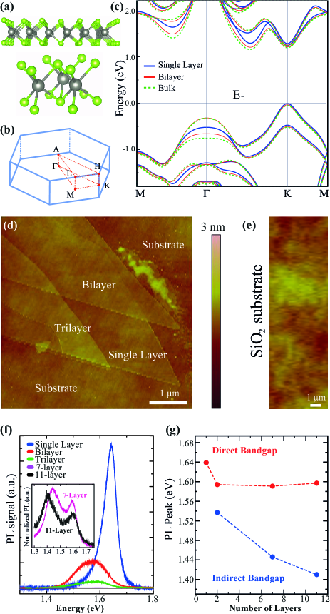
Electronic band structure calculations for bilayer and monolayer WSe2 show that the band gap increases from 1.21 eV in bulk to 1.23 eV (direct-indirect almost degenerate) for bilayer and 1.25 eV (direct) for monolayer WSe2 Fig. 1(c). Experimentally observed PL signal for bulk, bilayer and monolayer WSe2 peaks at 1.57, 1.57 and 1.64 eV, respectively (Fig.1(f)). We see that in contrast to the general case, for WSe2, LDA and GGA band dispersions differ significantly. While GGA finds single layer WSe2 as a semiconductor with a direct bandgap of 1.56 eV, LDA gives indirect bandgap of 1.68 eV. Here, both LDA and GGA finds VBM at the K symmetry point and CBM is located at K (in between and K) point in GGA (LDA). It appears that the GGA exchange correlation better approximates the ground state characteristics of the WSe2 crystal structure.
Here it is also worth to note that spin-orbit interaction results in two significant effects on the electronic band dispersion: (i) shifting down the valence band energies at the point (ii) band splitting at the vicinity of K and M symmetry points. Clearly, the existence of an intrinsic electric field breaks the inversion symmetry in the crystal structure. Therefore, it is seen that the degeneracy of the doubly degenerate valence and conduction bands of single layer WSe2 are removed by spin-orbit interaction and a band splitting occurs. Furthermore, when the spin-orbit interaction is taken into account in our calculations, conduction band edges at K and K- points show band splitting that allows various direct and indirect transitions (even in few-layered WSe2 structures). In our study, all the band structure calculations presented are performed by considering spin-orbit interaction together with GGA.
Previously, indirect to direct band crossover has been observed in other transition metal dichalcogenides PRL-105 ; sefamose2 ; SeydaMoSe2 and is consistent with our results. However, we note that the indirect to direct transition is rather steep for MoS2 where it’s bilayer form is an indirect band gap (1.6 eV) semiconductor while monolayer structure has a direct band gap (1.9 eV). In contrast, bilayer WSe2 possesses almost triple band gap degeneracy where the KK and K-K gap values are almost degenerate and the difference between first and second CBMs is (K)=40 meV which is close to thermal broadening (30meV). As a result of this band degeneracy, the integrated PL intensity (Fig. 1(e)) of bilayer WSe2 is of the same order of magnitude as in monolayers, i.e I1L/I2L 1-10, which compares with 100-1000 for MoS2. We also note that the PL signal for bilayer WSe2 is rather broad and can be described by at least two Lorentzian peaks. As the number of layers increases, the band degeneracy is gradually lifted, WSe2 becomes truly an indirect band gap semiconductor and the PL intensity decreases by orders of magnitude.
| WSe2 | -K | K | K K | K -K | (K) |
|---|---|---|---|---|---|
| Bulk | 1.48 | 1.52 | 1.25 | 1.21 | 0.04 |
| Bilayer | 1.51 | 1.52 | 1.24 | 1.23 | 0.04 |
| 1-Layer | 1.83 | 1.78 | 1.25(1.64) | 1.30 | 0.04 |
III.2 Anomalous Lattice Vibrations: Breaking the degeneracy of A1g and E2g modes at reduced dimensions
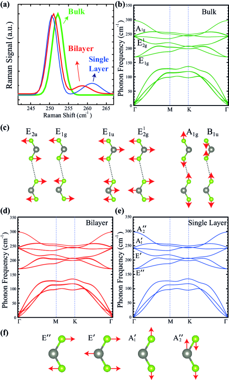
Next we turn our attention to the anomalous lattice vibrations of WSe2. For determination of lattice dynamics we use Raman spectroscopy which is one of the most useful non-destructive technique for the characterization of low-dimensional materials. Our measurements reveal that the most prominent Raman peak for bulk WSe2 is located at 252.2 cm-1 (Fig. 2(a)) while other semiconducting TMDs are characterized by well separated and Raman peaks. The stark difference between WSe2 and other TMDs already points towards an anomaly in the phonon dispersion of WSe2. Following from Fig. 2(b), calculated phonon dispersion confirms that bulk WSe2 displays only one strong vibrational mode around 250 cm-1 consistent with our experiments. Interestingly, for flakes thinner than four layers, an additional peak appears at roughly 5-11 cm-1 above the first order Raman peak. We find that the frequency difference between these two peaks is 5, 6 and 11 cm-1 for trilayer, bilayer, and monolayer WSe2 flakes, respectively. This peak is absent in few-layer flakes does not correspond to any new/additional Raman modes in the calculated phonon dispersion curve, which describes the Raman spectrum well.
Bulk and single layer WSe2 can be classified in the space group P63/mmc and P6m2, respectively. Similar to the MoS2 and MoSe2 counterparts,SeydaMoSe2 the unitcell of bulk WSe2 has eighteen phonon branches corresponding to six acoustic and twelve optical phonon modes. While the modes at 170 (300) cm-1 are 4-fold (2-fold) degenerate, six modes become almost degenerate at 250 cm-1 at the point. For a better understanding of the phonon spectrum and the prominent peak in the measurement, we present phonon symmetry representations of related modes and corresponding atomic motions in Figs. 2(b) and (c). It is seen that the 4-fold branch at 170cm -1 is formed by the vibrational motions corresponding to the E2u and E1g modes. Among these only the E1g mode is Raman-active. However, in backscattering experiments on a surface perpendicular to the c-axis, the E1g mode is forbidden and is not observed in our experiments. Furthermore, the decomposition of the six-fold phonon branch at 250 cm-1 (at point) can be described as . Among these the and modes are Raman-active and are degenerate in energy. As a result of this degeneracy, only one Raman peak can be observed in our measurements at 250 cm-1.
Next, we pay attention to the emergence of the second Raman peak in few and single layer WSe2 that appears 11 cm-1 above the main peak. Though, from bulk to single layer WSe2, there is no visible change in the calculated phonon dispersion (Figs. 2(b,d,e), our measurements show that a new peak develops (Fig. 2(a)) and this new peak appears to be very sensitive to the number of layers. For single layer WSe2, decomposition of the vibration representation is calculated to be . Here, the , and modes correspond to the , and modes for bulk respectively. Since the and modes are almost degenerate, only one Raman peak is expected to be observed in the experiment which contradicts our experimental results. Before discussing more on the discrepancy, we note that presence of contaminants at the WSe2/interface and/or directly bonded to the TMD monolayer might cause small alterations to the Raman spectrum. However, if the contaminants are directly bonded (chemisorption) to the TMD, one would expect to observe drastic differences in the Raman spectrum as a result of renormalization of phonon dispersion. Since the overall monolayer Raman spectrum is similar to few-layer, we eliminate this possibility. If the contaminants are chemically interacting locally, this would change the Raman signal from those local regions (Bloch waves intermix) but would be small comparing to overall Raman signal due to the geometrical considerations and reduced Raman sensitivity of the locally interacting region. To explain the emergence of the new peak, we consider external factors, such as compressive and tensile strain acting on few-layer and monolayer WSe2 flakes, which is likely to be induced by the interaction with the substrate.
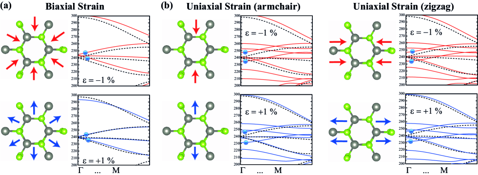
To test the possibility of strain effects on WSe2 as the origin for such splitting of the Raman peak, we calculate the phonon dispersion of monolayer WSe2 after applying 1 biaxial compressive and tensile strain. As seen from Fig. 3(a), such biaxial deformation only results in a collective softening/hardening of the vibrational modes and does not lift the degeneracy of the and modes ( and in single layer) implying that these modes remain degenerate as long as the hexagonal symmetry of the monolayer WSe2 is retained. Next, we apply uniaxial strain that is likely to occur along with the biaxial strain on monolayer WSe2 exfoliated on Si/SiO2 surface. For hexagonally ordered crystal structures uniaxial strain can be applied in two main directions: armchair and zigzag (Fig. 3(b)). Interestingly, in the presence of uniaxial strain, degeneracy of the branches forming the most prominent Raman peak are broken. While most of the modes between 200-280 cm-1 loose their symmetry that determines the Raman activity, our symmetry analysis shows that two of the branches that correspond to the (lower) and (upper) modes are still Raman active. For compressive (tensile) uniaxial strain along the armchair direction the difference between the and modes is 16 (18) cm-1. Similarly, for compressive (tensile) strain along the zigzag direction, splitting is calculated to be 13 (17) cm-1. Here the - splitting induced by uniaxial strain is in good agreement with our experimental data. It is worth to note that independent from the direction of both tensile and compressive strains both have the same splitting effect on the Raman peaks.
IV Discussions and Conclusions
According to our phonon dispersion calculations performed on bulk WSe2, the out-of-plane (A1g) and in-plane (E2g) modes are degenerate in energy, consistent with the experimental measurements taken on bulk WSe2. Experimentally, as the dimension is lowered from 3D to 2D (bulk to monolayers), Raman mode located at around 250 cm-1 splits in two peaks at 250 cm-1 and 261 cm-1. To provide an explanation for the broken degeneracy, we recalculate the phonon dispersion of monolayer WSe2 under uniaxial and biaxial strain/stress. Our theoretical results imply that the degeneracy of these two modes is lifted only if the crystal symmetry is broken, i.e. in the presence of uniaxial strain. When the monolayer WSe2 is under very little unaxial strain or stress, our theoretical calculations show a remarkable match with the experimental data. Considering above arguments, we next argue about the possible origin of uniaxial strain on thin WSe2 flakes. Since our SiO2 substrates typically display 4-8 Å surface roughness (Fig. 1(d-e)) that is of the same order of a single unit cell thickness, even perfect SiO2/WSe2 interface is likely to induce a mild strain to the WSe2 monolayer. The presence of the surface roughness on SiO2 can be observed clearly when compared to sapphire which yields only 1-2 Å surface roughness. Typically, these rough features are asymmetric in shape and therefore strain induced on the few-layer WSe2 is expected to have both biaxial and uniaxial component. However, since the biaxial strain does not lift the degeneracy only the uniaxial component of the total strain results in Raman peak splitting. Moreover, in the presence of residual contaminants at the WSe2/SiO2 interface and/or residues deposited after the exfoliation step, the effect of strain is likely to be amplified. From this perspective, monolayers are most affected by the strain effects while thick flakes remain mostly unaltered. Another scenario might be associated with the unintentional strain induced during the exfoliation process. In such case, the WSe2 monolayers are deposited on the SiO2 substrates during the exfoliation and is not necessarily related to the surface residue. However, we note that our results were confirmed on 50 different WSe2 monolayers where the same results have been found making this scenario. Another indirect confirmation of presence of uniaxial strain comes from the changes in the PL peak position. We also note that the band gap at the K-K symmetry point is expected to be independent from the dimensionality. On the contrary, PL measurements show that the K-K gap increases abruptly for the monolayer, likely due to the presence of small uniaxial strain (Fig. 1(g)) as is confirmed by our DFT calculations. We also point out that in the presence of large density of defects, the degeneracy can be lifted. However, similar measurements taken on more than fifty independently prepared samples makes this case unlikely.
In conclusion, phonon dispersion and the electronic properties of bulk to monolayer WSe2 have been studied both experimentally and theoretically. Unlike the other members of the TMDs, the and modes are degenerate in bulk WSe2 and the degeneracy is lifted for as the dimension is lowered. On the contrary to our experimental results, calculated phonon dispersion show that these modes remain degenerate independent from the dimensionality. However, theoretically the degeneracy is only lifted when the crystal symmetry is broken, i.e. in the presence of unaxial strain which might be induced by the interaction with the substrate, residues, and/or exfoliation process. These results provide deeper understanding in the vibrational properties of TMDs, especially on a material with unique phonon dispersion.
V Acknowledgements
This work was supported by the Flemish Science Foundation (FWO-Vl) and the Methusalem programme of the Flemish government. Computational resources were partially provided by TUBITAK ULAKBIM, High Performance and Grid Computing Center (TR-Grid e-Infrastructure). H. S. is supported by a FWO Pegasus Marie Curie Long Fellowship.
References
- (1) K. S. Novoselov, A. K. Geim, S. V. Morozov, D. Jiang, S. C. Dubonos, I. V. Grigorieva, and A. A. Firsov, Science 306, 666 (2004).
- (2) A. K. Geim and K. S. Novoselov, Nat. Mater. 6, 183 (2007).
- (3) X. Miao, S. Tongay, M. K. Petterson, K. Berke, A. G. Rinzler, B. R. Appleton, and A. F. Hebard, Nano Lett. 12, 2745 (2012).
- (4) F. Schwierz, Nature Nanotechnology 5, 487 (2010).
- (5) R. A. Gordon, D. Yang, E. D. Crozier, D. T. Jiang, and R. F. Frindt, Phys. Rev. B 65, 125407 (2002).
- (6) J. N. Coleman, M. Lotya, A. O’Neill, S. D. Bergin, P. J. King, U. Khan, K. Young, A. Gaucher, S. De, R. J. Smith, I. V. Shvets, S. K. Arora, G. Stanton, H. Y. Kim, K. Lee, G. T. Kim, G. S. Duesberg, T. Hallam, J. J. Boland, J. J. Wang, J. F. Donegan, J. C. Grunlan, G. Moriarty, A. Shmeliov, R. J. Nicholls, J. M. Perkins, E. M. Grieveson, K. Theuwissen, D. W. McComb, P. D. Nellist, and V. Nicolosi, Science 331, 568 (2011).
- (7) Q. H. Wang, K. Kalantar-Zadeh, A. Kis, J. N. Coleman, and M. S. Strano, Nature Nanotechnology 7, 699 (2012).
- (8) S. Tongay, S. S. Varnoosfaderani, B. R. Appleton, J. Wu, and A. F. Hebard, Appl. Phys. Lett. 101, 123105 (2012).
- (9) C. Ataca, H. Sahin, and S. Ciraci, J. Phys. Chem. C 116, 8983 (2012).
- (10) K. F. Mak, C. Lee, J. Hone, J. Shan, and T. F. Heinz, Phys. Rev. Lett. 105, 136805 (2010).
- (11) H. Peelaers and C. G. Van de Walle, Phys. Rev. B 86, 241401(R) (2012).
- (12) S. W. Han, H. Kwon,S. K. Kim, S. Ryu, W. S. Yun, D. H. Kim, J. H. Hwang, J.-S. Kang, J. Baik, H. J. Shin, and S. C. Hong, Phys. Rev. B 84, 045409 (2011).
- (13) J. K. Ellis, M. J. Lucero, and G. E. Scuseria, Appl. Phys. Lett. 99, 261908 (2011).
- (14) S. Tongay, J. Zhou, C. Ataca, K. Lo, T. S. Matthews, J. Li, J. C. Grossman, and J. Wu, Nano Letters, 12, 5576 (2012).
- (15) J. Kang, S. Tongay, J. Zhou, J. Li, and J. Wu, Appl. Phys. Lett. 102, 012111 (2013).
- (16) H. P. Komsa, J. Kotakoski, S. Kurasch, O. Lehtinen, U. Kaiser, and A. V. Krasheninnikov, Phys. Rev. Lett. 109, 035503 (2012).
- (17) W. Zhao, Z. Ghorannevis, L. Chu, M. Toh, C. Kloc, P.-H. Tan, and G. Eda, Acs Nano, 7, 791 (2013).
- (18) K. F. Mak, K. He, C. Lee, G. H. Lee, J. Hone, T. F. Heinz, and J. Shan, Nature Materials 12, 207 (2013).
- (19) J. Feng , X. Qian, C. Huang and J. Li, Nature Photonics 6, 866 (2012).
- (20) S. Horzum, H. Sahin, S. Cahangirov, P. Cudazzo, A. Rubio, T. Serin, and F. M. Peeters, Phys. Rev. B under publication (2013).
- (21) H. Fang, S. Chuang, T. C. Chang, K. Takei, T. Takahashi, and A. Javey, Nano Letters, 12, 3788 (2012).
- (22) P. E. Blochl, Phys. Rev. B 50, 17953 (1994).
- (23) G. Kresse and J. Hafner, Phys. Rev. B 47, 558 (1993).
- (24) J. P. Perdew, K. Burke, and M. Ernzerhof, Phys. Rev. Lett. 77, 3865 (1996).
- (25) S. Baroni, S. de Gironcoli, A. Dal Corso, and P. Giannozzi, Rev. Mod. Phys. 73, 515 (2001).
- (26) D. Alfe, Comput. Phys. Commun. 180, 2622 (2009).
- (27) Y. Y. Wang, Z. H. Ni, T. Yu, Z. X. Shen, H. M. Wang, Y. H. Wu, W. Chen, and A. T. S. Wee, J. Phys. Chem. C 112, 10637 (2008).
- (28) T. M. G. Mohiuddin, A. Lombardo, R. R. Nair, A. Bonetti, G. Savini, R. Jalil, N. Bonini, D. M. Basko, C. Galiotis, N. Marzari, K. S. Novoselov, A. K. Geim, and A. C. Ferrari, Phys. Rev. B 79, 205433 (2009).