Nanophotonic Computational Design
Jesse Lu∗ and Jelena Vučković
Stanford University, Stanford, California, USA.
jesselu@stanford.edu
Abstract
In contrast to designing nanophotonic devices by tuning a handful of device parameters, we have developed a computational method which utilizes the full parameter space to design linear nanophotonic devices. We show that our method may indeed be capable of designing any linear nanophotonic device by demonstrating designed structures which are fully three-dimensional and multi-modal, exhibit novel functionality, have very compact footprints, exhibit high efficiency, and are manufacturable. In addition, we also demonstrate the ability to produce structures which are strongly robust to wavelength and temperature shift, as well as fabrication error. Critically, we show that our method does not require the user to be a nanophotonic expert or to perform any manual tuning. Instead, we are able to design devices solely based on the user’s desired performance specification for the device.
OCIS codes: 230.75370, 130.3990.
References and links
- [1] J. Lu, J. Vuckovic, “Objective-first design of high-efficiency, small-footprint couplers between arbitrary nanophotonic waveguide modes,” Opt. Express 20, 7221-7236 (2012)
- [2] S. Boyd, N. Parikh, E. Chu, B. Peleato, and J. Eckstein, “Distributed Optimization and Statistical Learning via the Alternating Direction Method of Multipliers,” Foundations and Trends in Machine Learning 3, 1-122 (2011).
- [3] W. Shin and S. Fan, “Choice of the perfectly matched layer boundary condition for frequency-domain Maxwell’s equations solvers,” J. of Comp. Phys 231, 3406-3431 (2012).
- [4] S. Osher and R. Fedkiw, Level Set Methods and Dynamic Implicit Surfaces: 1st Edition (Springer, 2002).
- [5] Y. Jiao, S. Fan, and D. A. B. Miller, “Demonstrations of systematic photonic crystal design and optimization by low rank adjustment: an extremely compact mode separator”, Opt. Lett. 30, 140-142 (2005).
- [6] F. Van Laere, G. Roelkens, M. Ayre, J. Schrauwen, D. Taillaert, D. Van Thourhout, T. F. Krauss, and R. Baets, “Compact and highly efficient grating couplers between optical fiber and nanophotonic waveguides,” J. of Lightwave Tech. 25, 151-156 (2007).
1 Introduction
Currently, almost all nanophotonic components are designed by hand-tuning a small number of parameters (e.g. waveguide widths and gaps, hole and ring sizes). However, the realization of increasingly complex, dense, and robust on-chip optical networks will require utilizing increasing numbers of parameters when designing nanophotonic components.
Opening the design space to include many more parameters allows for smaller footprint, higher performance devices by definition, since original designs are still included in this parameter space. Unfortunately, the lack of intuition for what such designs might look like and the inability to manually search such a large parameter space have greatly hindered the ability to achieve this.
For this reason, we have developed and implemented a computational method which is able to use the full parameter space to design linear nanophotonic components in three dimensions. Critically, our method requires no user intervention or manual tuning. Instead, a design-by-specification scheme is used to produce designs based solely on a user’s performance specification.
We show that our method can indeed produce designs which are extremely compact, and, at the same time, highly efficient. Furthermore, we demonstrate that devices with novel functionality are easily designed. We also show that our method can be used to produce designs with extreme robustness to wavelength and temperature shift, as well as fabrication error.
Lastly, all our results are produced by simply specifying the functionality and performance of the desired device, which suggests that our method may indeed by able to design all linear nanophotonic devices.
2 Problem formulation
In order to produce designs which utilize the full parameter space, and are based solely on the user’s performance specification, we formulate the design problem in the following way:
| (1a) | ||||
| subject to | (1b) | |||
| (1c) | ||||
The explanation for the various terms in eq. (1) follows:
-
1.
is the physics residual for the th mode. That is to say, represents the underlying physics of the problem; namely, the electromagnetic wave equation .
The specific substitutions used in order to transform
are
-
•
,
-
•
,
-
•
, and
-
•
.
In contrast to typical schemes for optimizing physical structures, our formulation actually allows for non-zero physics residuals; which can be deduced since is not a hard constraint. Instead, this formulation is what we call an objective-first [1] formulation in that the design objective (explained below) is prioritized above satisfying physics.
-
•
-
2.
The (field) design objective consist of the constraint . Physically, this constraint describes the performance specification of the device via a series of field overlap integrals at various output ports of the device. Specifically, the terms represents an overlap integral between the E-field of the th mode () with an E-field of the user’s choice (), where the additional subscript allows the user to include multiple such fields. The amplitude of the overlap integral is then forced to reside between and .
This mechanism allows the user to express the desired performance of the device as a combination of field amplitudes in various output field patterns. These outputs would be in response to a predefined input excitation, which is determined by the current excitation () in the physics residual of each mode.
As an example of a design objective for some mode 1 a user might choose to have the majority of the output power reside in some output pattern 1, while ensuring that only a small amount of power be transferred to some output pattern 2. In this case the user would use for the former. and then for the latter; where and are representative of output patterns 1 and 2 respectively.
Finally, we note again that the design objective in our formulation is actually a hard constraint. This means that it is always satisfied, even to the extent of allowing for an unphysical field (since the physics residual will not be exactly 0). It is for this reason that we call such a formulation “objective-first”.
-
3.
The final term in eq. (1), , is the structure design objective. It is used as a relaxation of the binary constraint, , which would ensure that the final design be composed of two discrete materials.
3 Method of solution
We employed the alternating directions method of multipliers (ADMM) algorithm [2] in order to solve eq. (1). The ADMM algorithm solves eq. (1) by iteratively solving for , , and a dual variable .
Since we are working in three dimensions, solving eq. (1) for is non-trivial in that it involves millions of variables and requires solving for the ill-conditioned matrix. For this reason, we use a home-built finite-difference frequency-domain (FDFD) solver which implements a hardware-accelerated iterative solver[3] on Amazon’s Elastic Compute Cloud. Critically, our cloud-based solver allows us to scale to solve problems with arbitrarily-large number of modes, with no significant penalty in runtime.
In contrast to solving for , solving for is much simpler since we only consider planar structures; thereby limiting to have only thousands of variables.
Lastly, in order to arrive at fully discrete, manufacturable structures, we convert to a boundary parameterization[4] and tune our structure using a steepest-descent method.
4 Results
We demonstrate the effectiveness of our design method by producing designs for a variety of nanophotonic devices.
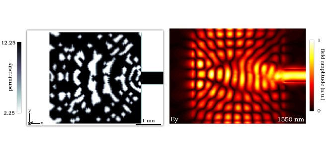
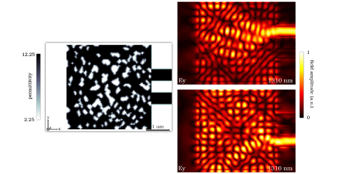
All of our results are in three dimensions and are planar structures, consisting of a 250 nm etched silicon slab completely surrounded by silica. The permittivity values of silicon and silica used were and respectively.
Many, if not all, of the produced designs exhibit novel functionality, high efficiency, and very compact footprints of only a few square vacuum wavelengths, while still remaining manufacturable. We also show that many devices can be designed to exhibit different functionality for different input excitations. Additionally, we show that devices can be designed with large tolerances for errors in wavelength, temperature and fabrication.
4.1 Mode converters
Our first devices consisted of waveguide mode converters. Such devices are simple in that they are single-input, single-output devices. At the same time, such a device is significant because it demonstrates the feasibility of multi-mode on-chip optical networks by showing that high-efficiency mode conversion can readily be achieved in planar on-chip nanophotonic structures.
We show, through the design of mode converters for both the TE- and TM-polarized waveguide modes, that our method is indeed fully three-dimensional. Additionally, the devices also demonstrate very small device footprints ( microns for this device in particular operating at 1550 nm wavelength).
4.1.1 TE mode converter
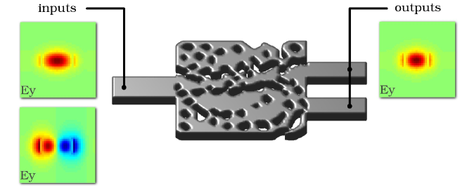
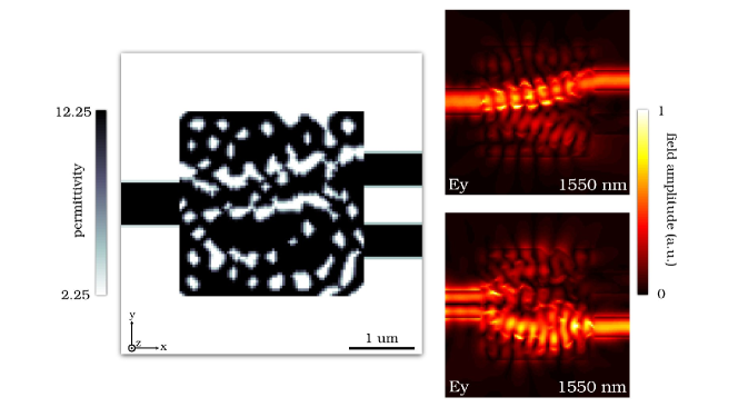
Our first result is a mode conversion device operating in the TE polarization, where the primary E-field component of the waveguide mode is polarized in the plane of the structure.
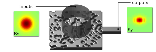
Our performance specification (fig. 1) for the device was for of the input power to be transferred from the fundamental waveguide mode, to the second-order waveguide mode. At the same time, we specified that no more than 1% of the input power was to remain in the transmitted fundamental mode.
The performance of the device is shown in fig. 2. The conversion efficiency into the second-order mode is lower than desired (86.4%). Imperfect conversion may be due to evanescent modes “interfering” with the output field overlap calculation.
4.1.2 TM mode converter
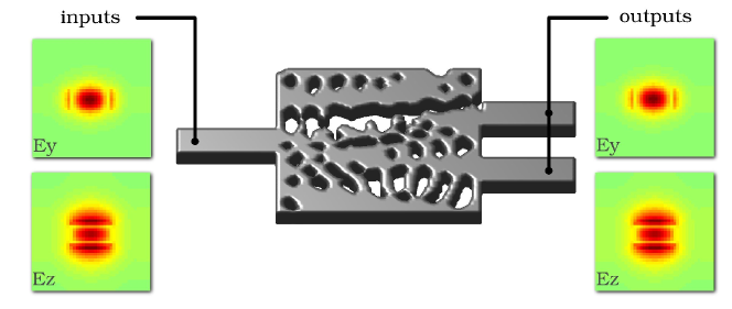
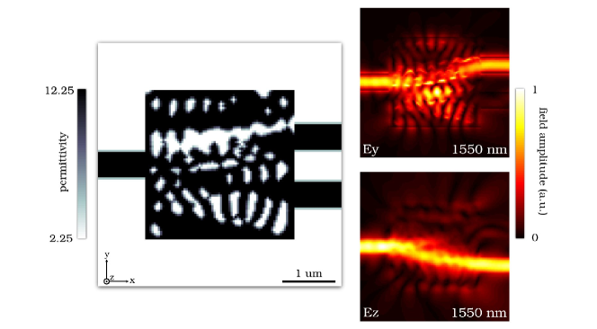
In addition to mode conversion in the TE polarization (E-field in-plane), we show that TM polarization (E-field out-of-plane) mode converters can be designed as well. This example shows that full three-dimensional structures truly are possible, and that no approximations are needed for our method.
Since our method is design-by-specification, the design of a TM mode converter requires only a small modification to the performance specification of the device; namely the polarization of the input and output modes (fig. 3). Specifically, we still design for conversion into the second-order mode and a allowance for the fundamental mode to be transmitted.
The performance of the device is shown in fig. 4. The lower conversion efficiency of 76.9% in contrast to the TE mode converter may be attributed to the lower confinement of the TM waveguide modes in such thin slabs. However, good rejection of only 1% is still achieved.
4.2 Mode splitters
Next, we demonstrate the design of nanophotonic waveguide mode splitters. Such devices can be used as multiplexers or demultiplexers and are the key component in utilizing a single waveguide to transmit multiple optical signals.
As a demonstration of the versatility of our method, we show that it is capable of designing mode splitting devices based on either the spatial profile, the polarization, or the wavelength of the input modes.
The performance specification for each device is simply to convert more than 90% of the input power in a particular input mode into either one of the output modes. At the same time, we specify that the transmission into the other output mode be kept below 1% of input power.
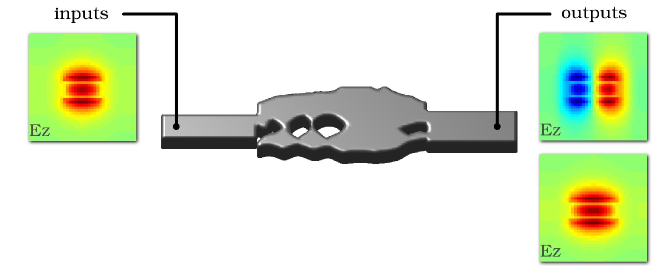
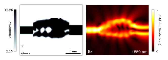
4.2.1 Spatial mode splitter
We demonstrate what is, to our knowledge, the first design for a three-dimensional nanophotonic spatial mode splitter (previous designs were restricted to two dimensions [5]). Such a device is the key enabler for multi-mode on-chip optical circuits, and we show here that they can be designed to be highly efficient while utilizing a very small device footprint ( microns). The performance specification is shown in fig. 5, and the final results is shown in fig. 6.
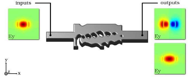
4.2.2 TE/TM splitter
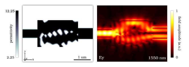
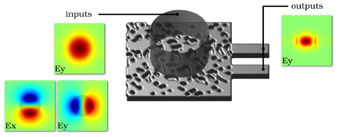
In addition to splitting different spatial modes, we show that different polarizations can also be split. Fig. 7 shows the performance specification of a device which is able to separate fundamental TE-polarized ( dominant) and TM-polarized ( dominant) waveguide modes into separate arms. The final, verified result is shown in fig. 8.
Not only is this result the first of its kind, it is the first in the device category where a single device is able to control both polarizations within the same device footprint. This shows the versatility and broad applicability of our method.
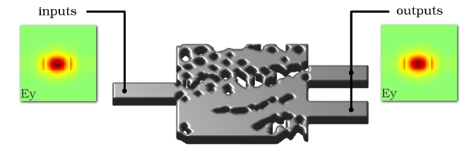
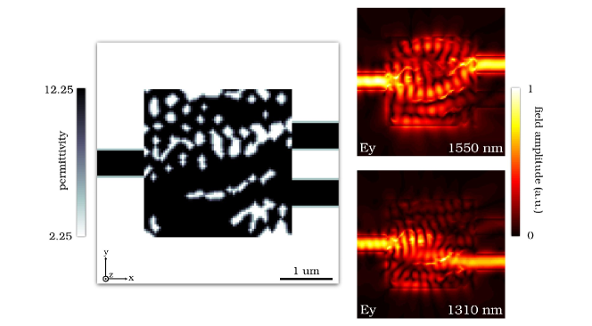
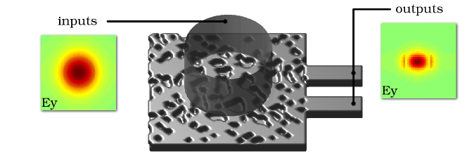
4.2.3 Wavelength splitter
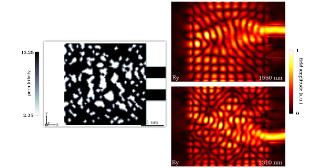
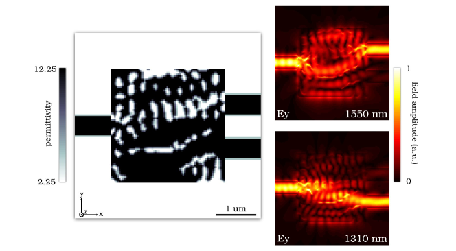
Traditional wavelength splitting devices can also be designed using our method. Here, we show that the 1550 nm and 1310 nm wavelengths can be split in a very small device footprint ( microns). The performance specification is shown in fig. 9, and the final result is shown in fig. 10.
4.3 Hubs
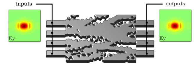
We continue to demonstrate the capabilities of our method by designing multi-input, multi-output devices which we call hubs. Such devices essentially re-arrange modes in the waveguides, and may be thought of as general cross-connect structures. Critically, the successful design of such structures shows that efficiently routing overlapping signals can be accomplished in a single layer for nanophotonic circuits.
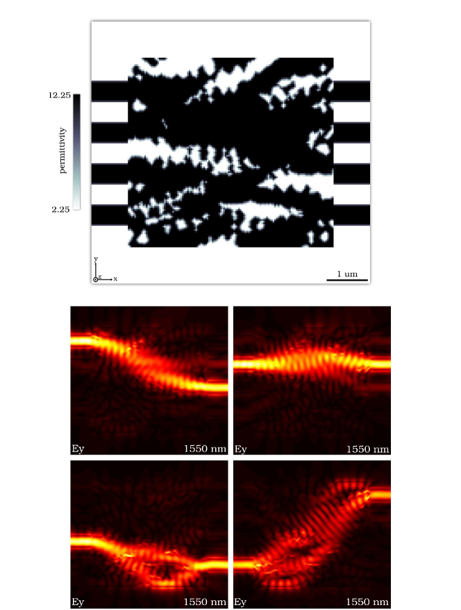
4.3.1 33 hub
We first design a hub with three inputs and outputs. The performance specification is shown in fig. 11, and the final result is shown in fig. 12.
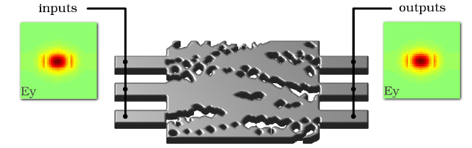
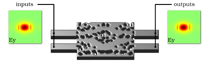
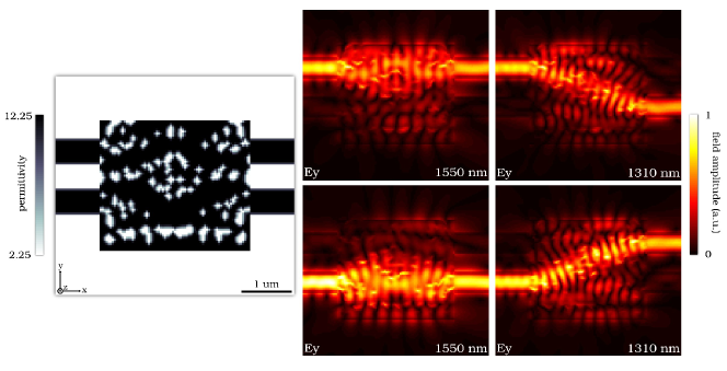
4.3.2 44 hub
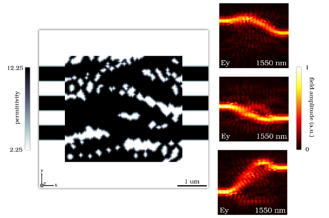
We extend our previous result to design a hub with four inputs and outputs. The performance specification is shown in fig. 13, and the final result is shown in fig. 14.
4.3.3 222 hub
We can now design a hub that performs different switching functions for different wavelengths. Specifically, we use two input waveguides, two output waveguides, and two wavelengths (hence the name 222).
Our performance specification (fig. 15) is to cross-couple the waveguides at the 1310 nm wavelength, but to uncouple the waveguides at the 1550 nm wavelength. The final result is shown in fig. 16.
4.4 Fiber couplers
The capabilities of our method are further demonstrated in the design of nanophotonic fiber couplers, which couple light from an optical fiber at normal incidence into an in-plane waveguide[6].
The structure of the optical fibers used was a 2 micron diameter core with refractive index , surrounded by a cladding with refractive index . The reduced size of the fiber core was employed in order to keep the device footprint small. Additionally, the fiber coupler devices were only etched to half the membrane depth, in order to increase the asymmetry in the device structure.
4.4.1 Compact fiber coupler
We first present the design of a compact fiber coupler. Such a device is said to be compact in that the functions of coupling into the plane, and focusing into a narrow waveguide are overlapped in the same device footprint.
Although the performance specification (fig. 17) desired a coupling efficiency above 90%, only 51.5% efficiency was achieved (fig. 18); however, this likely remains the highest efficiency demonstrated in a compact fiber coupler.
4.4.2 Mode-splitting fiber coupler
We now continue to show how different functionalities can be incorporated into a single device, by virtue of our design-by-specification scheme.
Here, we show how the functionality of a fiber coupler can be combined with that of a spatial mode splitter. Specifically, the performance specification (fig. 19) determines that different fiber spatial modes by split into different in-plane nanophotonic waveguides.
The final result (fig. 20) has lower efficiencies; however, the result is still useful in that no device with such a functionality has previously been demonstrated.
4.4.3 Wavelength-splitting fiber coupler
Another example of a functionality-combining device is the wavelength-splitting fiber coupler. Here, fiber modes of different wavelengths are coupled in-plane and then split into different nanophotonic waveguides (fig. 21). Once again, efficiencies are low (fig. 22), but no such device has previously been demonstrated.
4.5 Broadband wavelength splitter
We continue to investigate the capabilites of our method by attempting the design of a broadband wavelength splitter.
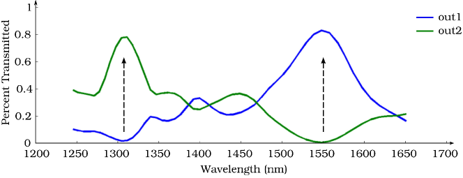
First, we revisit our wavelength splitter result (fig. 10) and perform a broadband analysis, the results of which are shown in fig. 23. This analysis reveals that device performance quickly drops off as one moves away from the target wavelengths.
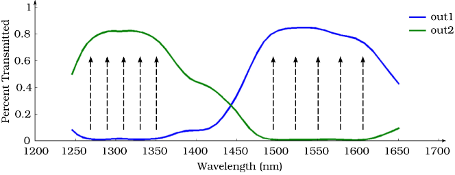
In order to design a broadband wavelength splitter, we modify our performance specification to include multiple target wavelengths (with identical desired performance) around the original target wavelengths, as seen in fig. 24 which reveals that broadband operation has been achieved. The final result for the broadband wavelength splitter is shown in fig. 25.
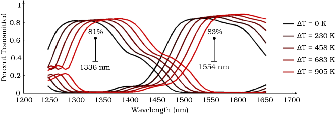
4.5.1 Temperature-robustness of broadband wavelength splitter
We can now perform a temperature analysis of our broadband wavelength splitter, using and (no refractive index shift for silica). This analysis, shown in fig. 26, reveals that stable operating points exist over a temperature range of nearly 1000 K. Such a result is telling in that it demonstrates that on-chip optical devices can be designed to be passively stable to temperature shifts which would typically be present in CPUs, since these are much less than 1000 K.
4.5.2 Fabrication-robustness of broadband wavelength splitter
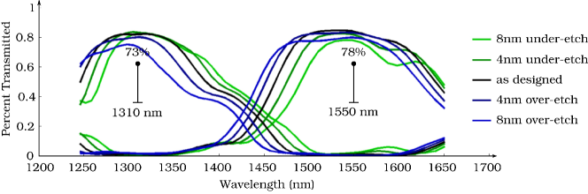
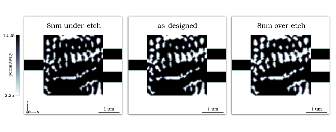
A analysis with regard to fabrication-error was also performed on the broadband wavelength splitter. The specific fabrication error was a general over- or under-etch of the device (input and output waveguides unaffected). Fig. 27 reveals that up to 8 nm of over- or under-etching can be sustained before performance falls below 70%, at the central operating wavelengths. The structural variations at 8 nm of etch error are shown in fig. 28.
This result is significant in that it demonstrates that the design of broadband devices seems to be a valid heuristic in the search for devices which are tolerant to temperature shifts and fabrication error. Note, however, that our method, as formulated, is also able to deal with temperature and fabrication shifts explicitly as well, although such results are not demonstrated here.
5 Conclusion
We have developed and implemented a method to design linear nanophotonic structures which are fully three-dimensional and multi-modal, have very compact footprints, exhibit high efficiency, and are manufacturable. We demonstrate this capability by designing various nanophotonic mode converters, splitters, hubs, and fiber couplers. Critically, many, if not all, of these devices have never been demonstrated before and cannot be designed by hand. In contrast, our method allows user to easily design such devices by virtue of our design-by-specification scheme.
In addition, we demonstrate the design of a broadband device
which is strongly robust to wavelength and temperature shift,
as well as fabrication error.
We show that such a device has stable operating wavelengths
over temperature shifts as large as 905 K,
or over-/under-etching error of up to 8 nm.
We suggest, based on this design, that wavelength tolerance
may be a good heuristic to the design of temperature and fabrication-error
tolerant nanophotonic devices.
This work has been supported by the AFOSR MURI for Complex and Robust On-chip Nanophotonics (Dr. Gernot Pomrenke), grant number FA9550-09-1-0704.