Properties of the defect modes in 1D lossy photonic crystals containing two types of negative-index-material defects
Abstract
In this paper, the characteristic matrix method is employed to theoretically investigate the propagation of electromagnetic waves through one-dimensional defective lossy photonic crystals (PCs) composed of negative index materials (NIMs) and positive index materials (PIMs). We consider symmetric and asymmetric geometric structures with two different types of NIM defect layers at the center of the structure. The effects of the polarization and the angle of incidence on the defect modes in the transmission spectra of both structures are investigated. The results show that the number of the defect modes within the photonic band gap (PBG) depends on the type of the NIM defect layer and is independent of the geometrical structure. Moreover, it is shown that the defect mode frequency increases as the angle of incidence increases. This property is also independent of the geometry of the structure. The results can lead to designing new types of narrowband and multichannel transmission filters.
I Introduction
Over the past two and half decades, a new class of material called photonic crystals (PCs) has emerged. The PCs originate from theoretical work of Yablonovitch, and John’s experimental work, which were published almost simultaneously in 1987 re1 ; re2 .The PCs are artificial dielectric or metallic structures in which the refractive index changes periodically in space. This kind of periodic structure affects the propagation of electromagnetic waves in the similar way as the periodic potential in a semiconductor crystal affects the electron motion by defining allowed and forbidden electronic energy bands. Whether or not photons propagate through PC structures depends on their frequency. Frequencies that are allowed to travel are known as modes, and groups of allowed modes form bands. Disallowed bands of frequencies are called photonic band gaps (PBGs) re3 ; re4 . These PBGs are also called the Bragg gaps because they originate from the Bragg scattering in the periodic structure. The properties of PBGs in one-dimensional (1D) PCs have been proven to play an important role in some potential applications such as photonic devices, optical filters, resonance cavities, laser applications, high reflecting omnidirectional mirrors, and the optoelectronic circuits re5 ; re6 ; re7 ; re8 .
By breaking the periodicity of the conventional PC structure, we will have a defective crystal. This can be performed by changing physical parameters, such as changing the thickness of one of the layer, adding another medium to the structure, or removing a layer from PCs re9 ; re10 ; re11 ; re12 ; re13 ; re14 . By introducing a layer with different optical properties, localized defect modes, which are also called resonant transmission peaks, can be generated within the PBG due to the change of the interference behavior of light re14 ; re15 , very similar to the defect states that are generated in the forbidden band of doped semiconductors. Upon prediction of the existence of materials with negative refractive index (NRI) in 1968 by Veselago re16 , such materials, which have negative permittivity and permeability simultaneously, have received extensive attention for their very unusual electromagnetic properties. Negative refractive index materials, or simply negative index materials (NIMs), are now also known as metamaterials. Recently, with the possibility of producing metamaterials, PCs with metamaterials, called metamaterial photonic crystals (MPCs) have been made.
In several papers the properties of the defect modes in different 1D conventional PC and 1D MPC structures have been investigated by introducing positive or negative indices defects re17 ; re18 ; re19 ; re20 ; re21 ; re22 ; re23 ; re24 ; re25 ; re26 ; re27 ; re28 ; re29 ; re30 ; re31 ; re32 ; re33 ; re34 ; re35 . Following the interesting report by Wu et al. re23 on the properties of the defect modes in 1D PCs with symmetric and asymmetric geometric structures, here we investigate the properties of the defect modes in the transmission spectra of 1D defective symmetric and asymmetric lossy MPCs which are composed of negative refractive index material defect layer at the center of the crystal. The outline of this paper is as follows. In Section 2, two geometric MPC structures, the permittivity and permeability of two types of NIMs, and also the characteristic matrix method and its formulation are presented. The numerical results and discussions are given in Section 3, and the conclusion is presented in Section 4.
II MPC structure and characteristic matrix method
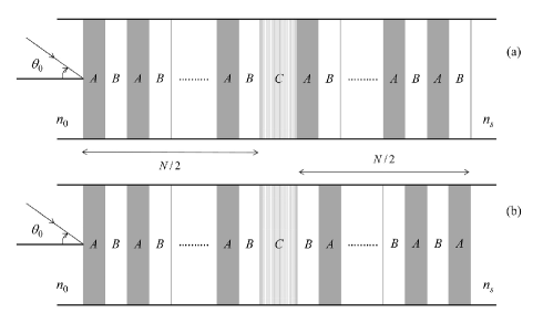
The 1D defective MPCs, which are constituted by alternative layers of NIM and positive index material (PIM), under study with asymmetric and symmetric structures in air with a defect layer at the center of the structures are shown in Figures 1(a) and 1(b), respectively, where NIMs are dispersive and dissipative. We assume that layers A and C (defect layer) are NIMs, and layer B is a PIM. N is the number of the lattice period, and also , , and () are thickness, permittivity and permeability of the layers, respectively.
The calculations are performed using the characteristic matrix
method re36 , which is the most effective technique to analyze
the transmission properties of PCs. The characteristic matrix for
, and symmetric
structures, are given by:
, and ,
where , and are the characteristic matrices
of layers A, B, and C. The characteristic
matrix for TE wave is given by re36 :
| (1) |
where, , c is speed of light in vacuum, is the ray angle inside the layer i with refractive index , , and , in which is the refractive index of the environment wherein the incidence wave tends to enter the structure. The refractive index is given as re31 ; re37 , where the positive and the negative signs are assigned for the PIM and NIM layers, respectively.
The final characteristic matrix for an N period structure is given by:
| (2) |
where are the matrix elements of . The transmission coefficient of the multilayer is calculated by:
| (3) |
In this equation, and , with being the refractive index of the environment where the wave leaves the crystal with angle . The transmissivity of the multilayer is given by . The transmissivity of the multilayer for TM waves can be obtained by using these previous expressions with , , and .
As mentioned before, our study is based on two different types of NIMs. The permittivity and permeability of type-I NIM layer with negative refracting index in the microwave region are complex, and are defined as re38 ; re39 ,
| (4) |
| (5) |
where f and are frequency and damping frequency in GHz, respectively. As mentioned in re39 , for GHz, the real parts of the permittivity and permeability, and , are simultaneously negative (double-negative material). For GHz, , but (single-negative material extending to the epsilon-negative material), and also for GHz, both and are positive (double-positive material). For type-II NIM layer, we use the Drude model re40 to describe the complex permittivity and permeability, with the results
| (6) |
| (7) |
Similarly, f and are respectively frequency and damping frequency, given in GHz. For GHz, both and , the real parts of the permittivity and permeability, are negative (double-negative material), and for GHz, , but (mu-negative material).
III Numerical results and discussion
Based on the theoretical model described in previous section, the transmission spectrum of the lossy defective PC with a NIM defect layer at the center is calculated. The calculations are carried out in the region where the real parts of the permittivity and permeability of two types of NIM layers (layers A, and C), and , are simultaneously negative where the zero- gap will appear re38 ; re39 ; re41 ; re42 . Equations (4) and (5), type-I NIM, are used for the permittivity and permeability of layer A. PIM layer (layer B) is assumed to be the vacuum layer with . The thickness of layers A, B, and C are respectively chosen as mm, mm, and mm. Also, the total number of the lattice period is selected to be re39 .
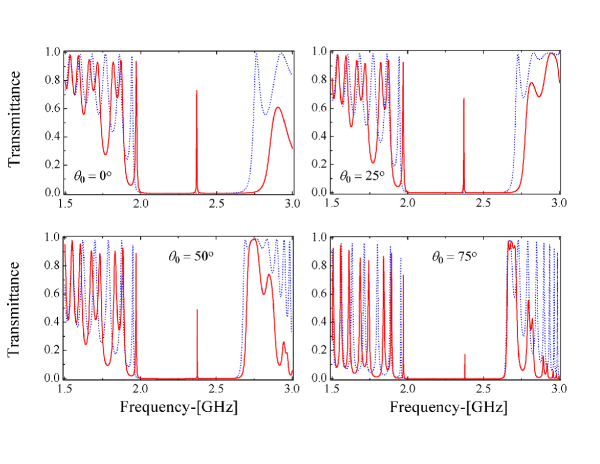
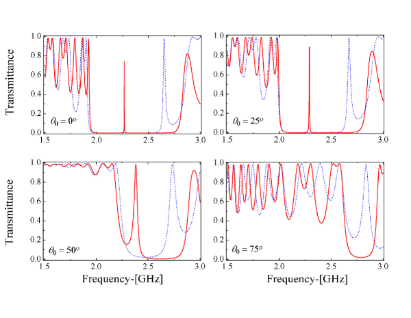
In the first part, we use equations (4) and (5), type-I NIM, for the permittivity and the permeability of NIM defect layer (layer C) exactly like layer A, and the transmission spectra of two different asymmetric and symmetric geometric structures for both polarizations are investigated. First of all, the transmission spectra of TE and TM polarized waves for the asymmetric structure at various angles of incidence and for GHz are shown in Figures 2 and 3. As it is seen, a single resonant peak appears within the PBG, which corresponds to the type-I NIM defect layer. This is in line with the report by Wu et al. re23 for the defect modes in 1D PCs with PIMs where only one defect mode for the asymmetric structure has been observed. In addition, the figures show that as the angle of incidence increases, the peak height of the defect mode decreases for TE waves and increases for TM waves. Moreover, for both polarizations the frequency of the defect mode is shifted to the higher frequency as the angle increases.
In Figures 4 and 5 we have plotted the frequency-dependent transmittance for the symmetric structure in TE and TM waves at four different angles of incidence. As it is observed in these figures, similar to the asymmetric structure, there is a single defect mode within the band gap again. This is in sharp contrast to the work by Wu et al. re23 for the defect modes in 1D symmetric PC with PIMs where there are two defect modes. It is also worth mentioning that the number of defect modes appearing with type-I NIM defect layer does not depend on the geometric structure, polarization, and angle of the incidence wave.
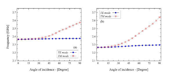
In more detail, as shown in Figure 6, the frequency of defect mode versus the angle of incidence for asymmetric (Figure 6(a)) and symmetric (Figure 6(b)) structures have been respectively plotted. As we mentioned earlier, only one defect mode appears in both asymmetric and symmetric structures. Additionally, as seen from the figures, in the asymmetric structure the defect modes appear in higher frequencies compared to the symmetric one. Another feature in Figure 6 which is worth mentioning is the frequency of the defect mode, which, in TE waves, remains nearly unchanged in both geometric structures as the angle of incidence increases. However, in TM waves, the frequency increases as the angle of incidence increases. In addition, this increase in symmetric structure is higher than that of asymmetric one.
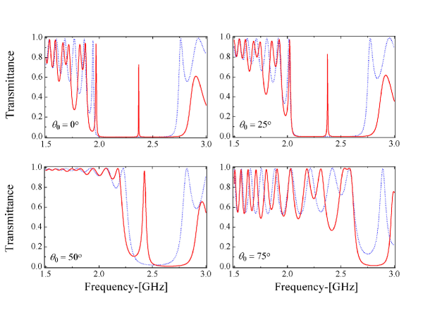
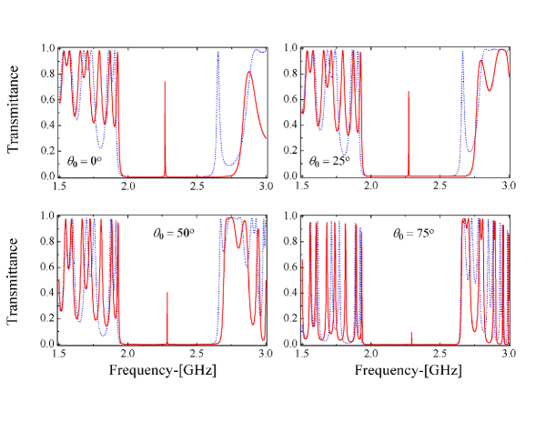
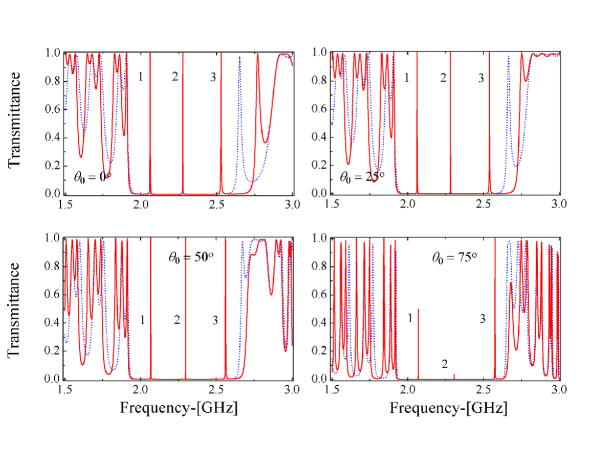
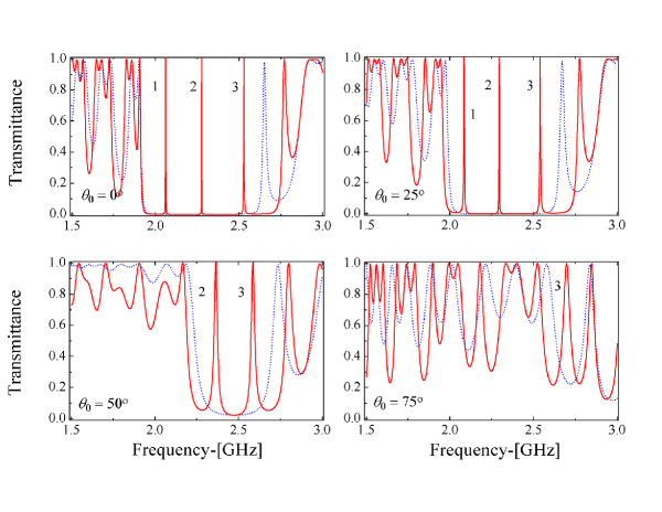
In the second part, properties of the defect mode of both geometric structures with another type of NIM defect layer at the center (type-II NIM), which was described in Section 2, are investigated. The asymmetric and symmetric structures which were used before are modified by replacing type-II NIM defect layer (layer C), in which the permittivity and permeability follow the equations (6) and (7). The other parameters are kept the same as the first part.
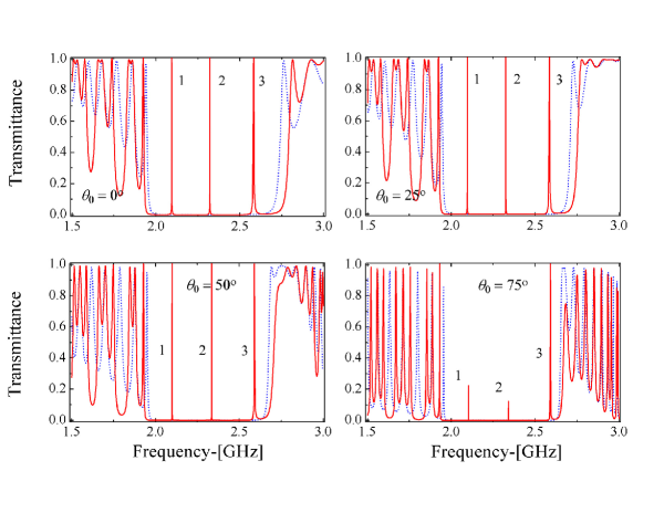
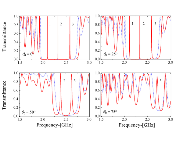
In Figures 7 and 8, we have respectively plotted the transmission spectra of TE and TM waves for the asymmetric structure at various angles of incidence, when the loss factors of two types of NIMs, layer A and C, are equal to GHz. We observe that there are three defect modes for both TE and TM waves, as identified by numbers 1, 2, and 3, respectively. Additionally, the transmission spectra of TE and TM waves for the symmetric structure have been plotted in Figures 9 and 10, respectively. In the symmetric structure, similar to the asymmetric one, there are three defect modes again. It can be seen from Figures 7 to 10 that the frequencies of the defect modes are shifted to the higher frequency as the incidence angle increases. Besides, these figures show that for both asymmetric and symmetric structures, three defect modes appear, which are independent of the geometry of the structure. To the contrary, as mentioned by Wu et al. re23 , in the conventional PCs case for a PIM defect layer, the symmetric geometric structure shows two defect modes and the asymmetric one shows one defect mode.
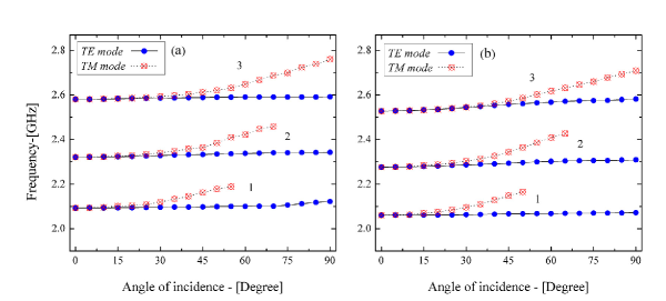
In more detail, we have plotted the defect mode frequency versus angle of incidence for both asymmetric (Figure 11(a)) and symmetric (Figure 11(b)) structures. As seen from these figures, in TE waves for both geometric structures, the frequency of defect modes remains nearly unchanged with increasing the angle of incidence. On the other hand, frequency of defect modes in TM waves increases as the angle of incidence increases. Additionally, similar to the first part, in the asymmetric structure the defect modes appear in higher frequencies compared to the symmetric one. In contrast to type-I NIM defect layer, frequencies of defect modes, which increase in the asymmetric structure, are higher than that of the symmetric structure. Another feature in Figure 11 is that in the asymmetric structure, defect modes 1 and 2 disappear for angles more than and , respectively. Also, defect modes 1 and 2 disappear for angles more than and , respectively, in the symmetric structure. To the contrary, Figure 6, by comparing defect mode 3 in both geometric structures for TM waves, shows that the frequency of the defect mode in the asymmetric structure changes more than that of the symmetric one.
As we observe, in comparison to the first part, which is type-I NIM defect layer, the number of defect modes depends on the types of NIMs which are being used for the defect layer. In addition, as the figures show, for two types of NIMs, the number of defect modes does not depend on the geometric structure. This is in sharp contrast with the work done by Wu et al. re23 where the number of defect modes depends on the asymmetric or symmetric structure.
IV Conclusion
This paper has theoretically investigated the properties of defect modes coming from two types of NIMs defect layer at the center of 1D defective lossy MPCs in symmetric and asymmetric geometric structures. Our numerical results show that there exists a single defect mode inside the PBG in both asymmetric and symmetric structures for TE and TM polarized waves, when the type-I NIM defect layer is considered. On the other hand, the results show that with changing the types of NIMs in the defect layer, we observe three defect modes inside the band gap for both structures. Positions (frequencies) of the defect modes depend on the polarization of the waves and the incidence angles. As the incidence angle increases, the frequency of the defect modes moves toward higher frequencies regardless of the geometrical structures and types of NIMs defect layer. Additionally, the results of this study bring up the conclusion that the number of defect modes in 1D asymmetric and symmetric lossy PCs strongly depends on the types of NIM defect. Besides, an important result is that by using an NIM in the structure of PCs, the defect modes show different behavior from that of the PCs with only PIMs. Finally, it is worthwhile to mention that the number of defect modes does not depend on the asymmetric or symmetric structures, contrary to the work conducted by Wu et al. re23 . Detailed analysis of the defect modes in metamaterial photonic crystals with different geometric structures will certainly provide useful information for designing new types of narrowband and multichannel transmission filters.
Acknowledgements.
A. Aghajamali would like to acknowledge his gratitude to P. Shams for her help and useful discussion.References
- (1)
References