Positional dependence of energy gap on line defect in armchair graphene nanoribbons: Two-terminal transport and related issues
Abstract
The characteristics of energy band spectrum of armchair graphene nanoribbons in presence of line defect are analyzed within a simple non-interacting tight-binding framework. In metallic nanoribbons an energy gap may or may not appear in the band spectrum depending on the location of the defect line, while in semiconducting ribbons the gaps are customized, yielding the potential applicabilities of graphene nanoribbons in nanoscale electronic devices. With a more general model, we also investigate two-terminal electron transport using Green’s function formalism.
pacs:
73.22.Pr, 71.55.-i, 73.22.-f, 73.23.-bI Introduction
The fabrication of single layer graphene by Novoselov et al. novoselov in 2004 has opened a new era in the research of low-dimensional nanostructured materials. Graphene, the carbon allotrope with planar honeycomb lattice structure, is a promising candidate of nano-electronic components owing to its exceptional electronic, thermal and transport properties neto . It has been predicted that graphene sheet is a zero gap semiconductor abergel , but its behavior strongly depends on the boundary conditions when it is tailored into ribbon, flake or tube we1 . The sensitivity to the ribbon width, chirality, shape of the edges has allowed one to switch its semiconductor-like behavior from zero gaped to the finite one. Intensive researches have already been done on graphene nanoribbons (GNRs) to explore the influence of edge topology barone ; nakada on transport properties. Some attempts including chemical doping ouyang ; huang , application of uniaxial strain sena ; chang , chemical edge modifications wang , incorporation of impurity tsuyuki , line defect lahiri ; lin ; okada ; gunlycke ; costa are in focus of study on this system. But to realize the potential application of this material the control over transport properties needs to be clarified in a deeper way.
To date, many theoretical fujita ; waka ; schulz as well as experimental han ; cooper works have been done which reveal the fact that graphene nanoribbons (GNRs) with zigzag edges exhibit a metallic phase with localized states located on the edges, while armchair graphene nanoribbons (AGNRs) show metallic or semiconducting phase depending on the width of the ribbons zheng ; son ; chen . This phenomenon is true only for clean ribbons i.e., without any deformation anywhere in the sample. But, the presence of impurity or deformation makes the system behave differently. In 2007 Peeters et al. costa have shown that in presence of line impurity in graphene nanoribbon a gap opens up in the energy band spectrum. The system they considered was practically coupled two graphene ribbons of different sizes separated by a distance. Line defect also yields the possibility of using graphene as a valley filter as demonstrated by Gunlycke et al. gunlycke . In a recent experiment topological line defect has been studied using scanning tunneling microscope lahiri ; okada . Although the studies involving AGNRs have already generated a wealth of literature there is still need to look deeper into the problem to address several important issues those have not been
well explored earlier, as for examples the understanding of the behavior of energy gap in metallic and semiconducting AGNRs in presence of line defect and also the dependence of this energy gap on the location of line defect. In the present work we mainly concentrate on these issues. Here we analyze the energy band structure of simple armchair graphene nanoribbons in presence of line defect within a tight-binding model. We show that depending on the location of a line defect in a metallic AGNR an energy gap may or may not appear in the band spectrum, while in a semiconducting AGNR the gap can be controlled. This phenomenon leads to the possibility of using AGNRs as nanoscale electronic devices. With a more specific model we also describe two-terminal electron transport through finite sized AGNRs by attaching them to two semi-infinite graphene leads using Green’s function formalism to explore the results in realistic cases.
The structure of the paper is as follows. In Section II, we describe the specific model i.e., AGNR with side-attached leads and theoretical formulation to illustrate two-terminal electronic transport. The essential results are presented in Section III which contains (a) energy band structure of simple isolated armchair graphene nanoribbons in presence of line defect, and (b) transmission probability as a function of injecting electron energy through the lead-AGNR-lead bridge system. Finally, in Section IV, we summarize our main results and discuss their possible applications for further study.
II Model and theoretical formulation
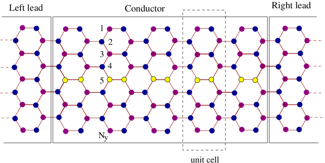
Model: Figure 1 presents a schematic illustration of the model quantum system, where a finite size AGNR is coupled to two semi-infinite graphene leads with armchair edges. The blue and magenta circles correspond to two different sublattices of the ribbon, and, the yellow circles, representing the defect sites, are arranged in a line result a defect line. A unit cell of the AGNR is described by the dashed region which contains atomic sites in our notation.
Our analysis for the present work is based on non-interacting electron picture, and, within this framework, tight-binding (TB) model is extremely suitable for analyzing electron transport through such a two-terminal bridge system. The single particle Hamiltonian which captures the AGNR and side-attached leads gets the form:
| (1) |
The first term denotes the Hamiltonian of the AGNR sandwiched between two graphene leads. Under nearest-neighbor hopping approximation, the TB Hamiltonian of the AGNR reads,
| (2) |
where, is the on-site energy and is the nearest-neighbor hopping integral. The hopping integral is set equal to or whether an electron hops between two ordered atomic sites or between two defect sites, and it is when the hopping of an electron takes place between an ordered and a defect site. () is the creation (annihilation) operator of an electron at the site .
The second and third terms of Eq. 1 correspond to the Hamiltonians for the semi-infinite graphene leads (left and right leads) and AGNR-to-lead coupling. A similar kind of TB Hamiltonian (see Eq. 2) is used to illustrate the leads where the Hamiltonian is parametrized by constant on-site potential and nearest-neighbor hopping integral . The AGNR is directly coupled to the leads by the parameters and , where they (coupling parameters) correspond to the coupling strengths between the edge sites of the ribbon and the left and right leads, respectively.
Transmission probability: To obtain electronic transmission probability through the AGNR we use Green’s function formalism. Within the regime of coherent transport and in the absence of Coulomb interaction this technique is well applied. Using Fisher-Lee relation, two-terminal transmission probability through the lead-AGNR-lead bridge system can be written as datta1 ,
| (3) |
where, and are the coupling matrices and and are the retarded and advanced Green’s functions of the AGNR, respectively. Now the single particle Green’s function operator representing the entire system for an electron with energy is defined as,
| (4) |
where, , represents the Hamiltonian of the full system and is the identity matrix. Following the matrix forms of and , the problem of finding in the full Hilbert space of can be mapped exactly to a Green’s function corresponding to an effective Hamiltonian in the reduced Hilbert space of the AGNR itself and we get datta1 ,
| (5) |
Here, and are the contact self-energies introduced to incorporate the effect of coupling of the AGNR to the left and right leads, respectively. Below we represent explicitly how these self-energies are evaluated for the graphene leads attached to the AGNR.
Evaluation of self-energy: In order to determine self-energies for these side-attached leads we follow the prescription
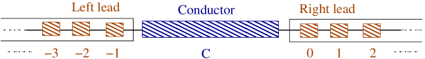
addressed by Sancho et al. sancho , where both leads and AGNR are sketched with discrete effective principal layers. These layers are defined as the smallest group of neighboring atomic planes and they allow only nearest-neighbor interaction between them. It effectively transforms the original system into a linear chain of principal layers nardelli as shown in Fig. 2. We label the principal layers in the right-lead as , , , and in the left-lead as , , , and so on. The sample between the leads is denoted by . Below, we describe elaborately the evaluation of the self-energy corresponding to the right lead, and, following this prescription we also determine the self-energy for the left lead. Using Eq. 4 a set of equations for the layer orbitals can be written as,
where, we assume that and . Here, describes the Hamiltonian of -th principal layer, while corresponds to the coupling matrix between -th and ()-th layers. The general expression of reads,
| (7) |
where,
| (8) |
Substituting into the expressions of and we can write,
| (9) |
and this process continues iteratively to repeat. After -th iteration we have,
| (10) |
with,
| (11) |
The iteration is to be done until , with arbitrarily small.
Using these ’s we can determine the Green’s function of a single layer in terms of the Green’s function of the following or preceding one like,
| (12) |
where, is the transfer matrix and it is defined as,
| (13) |
After some algebraic calculations we can write from Eq. LABEL:greeneq,
| (14) |
With this formalism, the surface Green’s function of the left and right leads can be found as,
| (15) |
where, and are the Hamiltonians for a principal layer in both layer and the tunneling matrix between two principal layers in the right-lead, respectively. The main advantage of this framework meunier ; jodar ; farajian rather than any other method is that here the number of iterations required for convergence is very small li ; shokri . Finally, we get the expressions for the self-energies of the two leads as,
| (16) |
where, and are left lead-to-AGNR and AGNR-to-right lead coupling matrices, respectively. Using the above expressions of self-energies for the graphene leads we evaluate effective Green’s function with the help of Eq. 5 and then calculate two-terminal transmission probability.
III Results and Discussion
In this section we present analytical results of energy band spectrum for isolated AGNRs and numerical results computed for transmission probability through AGNRs under conventional biased conditions. Throughout our analysis we set the on-site energies in the two side-attached graphene leads to zero, , and in the AGNR for ordered sites, while eV for defect sites. The nearest-neighbor coupling strength in the leads () is fixed at eV, and the coupling parameters and are also set at eV. In AGNR, sandwiched between two leads, we use three different hopping integrals, , and , and their values are fixed at eV, eV and eV, respectively. We fix the equilibrium Fermi energy at zero and choose the units where . The energy scale is measured in unit of .
III.1 AGNR without side-attached leads: Energy band structure and related issues
To find the energy dispersion relation of an infinitely extent (along -direction) AGNR, having a finite width along -direction, we establish an effective difference equation analogous to the case of an infinite one-dimensional chain. This can be done by proper choice of a unit cell (for example, see the unit cell configuration presented by the dashed region in Fig. 1) from the nano-ribbon. With this configuration, the effective difference equation of the AGNR reads,
| (17) |
where,
| (25) |
In the above relation, and correspond to the site-energy
and nearest-neighbor hopping matrices of the unit cell, respectively, and is the identity matrix. The dimension of these three matrices is (). Since in the nano-ribbon translational invariance exists along the -direction, we can write in terms of the Bloch waves and then Eq. 17 gets the form,
| (26) |
where, is the spacing between two neighboring unit cells. is the length of each side of hexagonal benzene like ring. Solving Eq. 26 we find the desired energy dispersion relation ( vs. ) of the armchair ribbon.
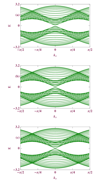
As illustrative examples, in Fig. 3 we present the energy band diagrams of AGNRs for three different ribbon widths when they are free from any line defect. In this spectra the three typical numbers (, and ) of are chosen only to make in the forms , and , respectively, since the energy band structures of
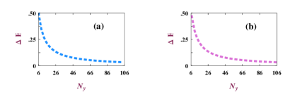
AGNRs are highly sensitive to these typical ribbon widths zheng . Here we set . From the spectra it is observed that for the particular case where , the lowest conduction band and the highest valence band coincides with each other at , resulting zero energy gap in the band spectrum (Fig. 3(c)). This indicates metallic phase of the AGNR. However, for the other two cases ( and ), a finite gap in the band spectrum is obtained at representing the semiconducting behavior. In these three spectra (Figs. 3(a)-(c)) since is finite, the wavevector along -direction becomes quantized and for each value of we get a - curve which results distinct energy levels in the - diagram. For large enough , energy gaps between these energy levels decrease sharply, and therefore, quasi-continuous energy bands are formed. The energy gaps between the conduction and valence bands, at , of AGNRs with and strongly depend on the value of i.e., ribbon width. To reveal this fact in Fig. 4 we present the variation of energy gap as a function of for two different cases. It shows that the energy gap sharply decreases with when becomes smaller, but it eventually saturates to a finite non-zero value, though it is too small, for large enough . So, in short, we can emphasize that a metallic phase is observed for AGNRs when , while the semiconducting phase is visible for the AGNRs with and .
The results described above for clean nanoribbons i.e., nanoribbons in absence of any line defect have already been established in the literature, but the central issue of our present investigation - the interplay between the existence of a line defect, the width of AGNRs and the location of line defect has not been well addressed earlier.
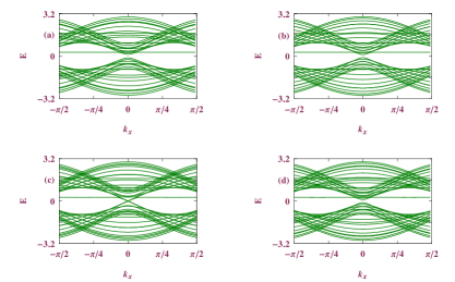
To explore it, we present in Fig. 5 the energy band diagrams for some typical AGNRs in presence of a line defect, where the defect sites
are described by the yellow circles as shown in Fig. 1. The location of a line defect is described by the variable and we assign for the edge of an AGNR. In Figs. 5(a) and (b) the results are shown for the ribbon widths and , respectively, and both for these two cases a finite energy gap around is obtained which reveals the semiconducting nature. The situation is somewhat interesting when the width of the AGNR gets the form . The results are shown in Figs. 5(c) and (d) where we choose () and locate the defect lines at and , respectively. In one case a sharp crossing between the energy levels takes place at , results a metallic phase, while for the other case a finite energy gap opens up for this typical value of revealing the semiconducting phase. Thus, a metallic AGNR (width ) can exhibit a metallic or a semiconducting phase depending on the location of a impurity line in the ribbon. In a metallic AGNR two types of states, metallic and semiconducting, for carbon chains exist which result these two types of conducting phases depending on the location of line defect, while a semiconducting AGNR contains only semiconducting chains, and accordingly, it does not provide the metallic behavior in presence of a line defect.
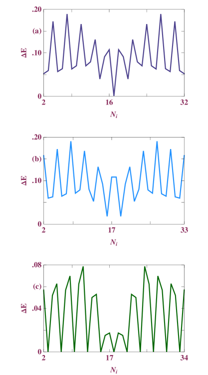
The energy gap , across , strongly depends on the structural details i.e., the location of defect line in the nanoribbon.
As illustrative example, in Fig. 6 we show the variation of as a function of impurity position for three different ribbon widths. It shows an oscillating behavior with the position of the defect line. For the semiconducting AGNRs (Figs. 6(a) and (b)) the energy gap never drops to zero (for the energy gap in Fig. 6(a) becomes very small, but still it has a finite non-zero value which results a semiconducting phase), while for the metallic ribbon (Figs. 6(c)) exactly vanishes when becomes equal to , being an integer. These phenomena promote a design concept based on the structural details as semiconducting devices with variable energy band gaps.
III.2 AGNR with side-attached leads: Two-terminal transmission probability and ADOS
Keeping in mind a possible experimental realization of the system, we clamp a finite sized armchair graphene nanoribbon between two ideal semi-infinite graphene leads (the left and right leads) making a lead-AGNR-lead bridge (see Fig. 1). Below we present our numerical results for average density of states (ADOS) and two-terminal transmission probability through finite sized AGNRs under conventional biased conditions.
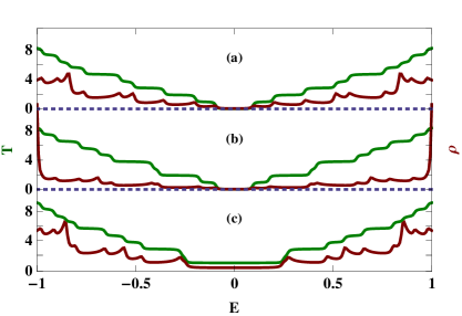
In Fig. 7 we show the variation of transmission probability, , together with the average density of states (ADOS), , as a
function of energy for some typical finite sized AGNRs in the absence of any line defect, where (a), (b) and (c) correspond to the results for , and , respectively. Here we set and choose twenty unit cells. Our previous analytical arguments for the AGNRs are exactly corroborated in these diagrams. A finite energy gap in the transmission probability associated with the energy gap in ADOS spectrum is obtained when becomes identical to and , as shown in Figs. 7(a) and (b). This behavior emphasizes the semiconducting phase for these ribbon widths. On the other hand a gap less spectrum is observed when becomes equal to (Fig. 7(c)), which indicates the metallic phase of the AGNR.
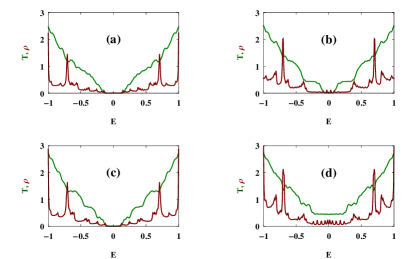
Finally, we describe the results shown in Fig. 8, where we present transmission probability and ADOS for some typical AGNRs in presence of single line defect. In (a) and (b) the results are presented for and , respectively, and for both these two cases transmission function shows a finite energy gap across exhibiting the semiconducting nature, with reduced amplitude compared to the spectra given in Fig. 7. The structural dependence on the conducting behavior in metallic AGNR () in presence of line defect is clearly visible from the spectra given in Figs. 8(c) and (d), where the defect lines are placed in the -th and -th lines, respectively. For the first case, it provides the semiconducting behavior, while in the other case the metallic phase is obtained, which perfectly corroborate our previous analytical findings.
IV Conclusion
To summarize, we have investigated in detail the characteristics of energy band spectrum of armchair graphene nanoribbons in presence of line defect within a simple non-interacting tight-binding framework. The essential results have been presented in two parts. In the first part we have presented analytical results of energy band spectrum for isolated AGNRs. From our analytical results we have analyzed that depending on the location of a line defect a metallic AGNR can provide either a metallic or a semiconducting phase, while a semiconducting AGNR provides only the semiconducting phase with variable band gap. In the second part, we have discussed numerical results for transmission probability together with ADOS, keeping in mind a possible experimental realization of the system. We have shown that our numerical results exactly corroborate the analytical findings. Though the results presented in this article are worked out at absolute zero temperature limit, the results should remain valid even at finite temperatures (K) since the broadening of the energy levels of the AGNR due to its coupling with the metal leads is much higher than that of the thermal broadening datta1 ; we2 ; we3 ; we4 ; we5 ; we6 ; we7 ; we8 .
Throughout our work, we have addressed the electronic transport properties in AGNRs for some typical parameter values. In our model calculations we chose them only for the sake of simplicity. Though the results presented here change numerically with these parameter values, but all the basic features remain exactly invariant.
References
- (1) K. S. Novoselov, A. K. Geim, S. V. Morozov, D. Jiang, Y. Zhang, S. V. Dubonos, I. V. Grigorieva, and A. A. Firsov, Science 306, 666 (2004).
- (2) A. H. C. Neto, F. Guinea, N. M. R. Peres, K. S. Novoselov, and A. K. Geim, Rev. Mod. Phys. 81, 109 (2009).
- (3) D. S. L. Abergel, V. Apalkov, J. Berashevich, K. Ziegler, and T. Chakraborty, Adv. Phys. 59, 261 (2010).
- (4) P. Dutta, S. K. Maiti, and S. N. Karmakar, Eur. Phys. J. B 85, 126 (2012).
- (5) V. Barone, O. Hod, and G. E. Scuseria, Nano Lett. 6, 2748, (2007).
- (6) K. Nakada, M. Fujita, G. Dresslhaus, and M. S. Dresslhaus, Phys. Rev. B 54, 17954 (1996).
- (7) Y. Ouyang, S. Sanvito, and J. Guo, Surf. Sci. 605, 1643 (2011).
- (8) B. Huang, Phys. Lett. A 375, 845 (2011).
- (9) S. H. R. Sena, J. M. Pereira Jr., G. A. Farias, F. M. Peeters, and R. N. Costa Filho, J. Phys.: Condens. Matter 24, 375301 (2012).
- (10) C. P. Chang, B. R. Wu, R. B. Chen, and M. F. Lin, J. Appl. Phys. 101, 063506 (2007).
- (11) Z. F. Wang, Q. Li, H. Zheng, H. Ren, H. Su, Q. W. Shi, and J. Chen, Phys. Rev. B 75, 113406 (2007).
- (12) H. Tsuyuki, S. Sakamoto, and M. Tomiya, arXiv:1207.5598.
- (13) J. Lahiri, Y. Lin, P. Bozkurt, I. I. Oleynik, and M. Batzill, Nature Nanotech. 5, 326 (2010).
- (14) X. Lin and J. Ni, Phys. Rev B 84, 075461 (2011).
- (15) S. Okada, T. Kawai, and K. Nakada, J. Phys. Soc. Japan 80, 013709 (2011).
- (16) D. Gunlycke and C. T. White, Phys. Rev. Lett. 106, 136806 (2011).
- (17) R. N. Costa Filho, G. A. Farias, and F. M. Peeters, Phys. Rev. B 76, 193409 (2007).
- (18) M. Fujita, K. Wakabayashi, K. Nakada, and K. Kusakabe, J. Phys. Soc. Japan 65 1920 (1996).
- (19) K. Wakabayashi, Y. Takane, M. Yamamoto, and M. Sigrist, Carbon 47, 124 (2009).
- (20) D. A. Bahamon, A. L. C. Pereira, and P. A. Schulz, Phys. Rev. B 83, 155436 (2011).
- (21) M. Y. Han, B. Ozyilmaz, Y. B. Zhang, S. Lee, and H. Dai, Science 319, 1229 (2008).
- (22) D. R. Cooper, B. D’Anjou, N. Ghattamaneni, B. Harack, M. Hilke, A. Horth, N. Majlis, M. Massicotte, L. Vandsburger, E. Whiteway, and V. Yu, arXiv:1110.6557v1.
- (23) H. Zheng, Z. F. Wang, T. Luo, Q. W. Shi, and J. Chen, Phys. Rev. B 75, 165414 (2007).
- (24) Y. -W. Son, M. L. Cohen, and S. G. Louie, Phys. Rev. Lett. 97, 216803 (2006).
- (25) X. Chen, H. Wang, H. Wan, K. Song, and G. Zhou, J. Phys.: Condens. Matter 23, 315304 (2011).
- (26) S. Datta, Electronic transport in mesoscopic systems, Cambridge University Press, Cambridge (1995).
- (27) M. P. López Sancho, J. M. López Sancho, and J. Rubio, J. Phys. F: Met. Phys. 14, 1205 (1984).
- (28) M. B. Nardelli, Phys. Rev. B 60, 7828 (1999).
- (29) V. Meunier and B. G. Sumpter, J. Chem. Phys. 123, 24705 (2005).
- (30) E. Jóder, A. Pérez-Garrido, A. Dýáz-Sánchez, Phys. Rev. B 73, 205403 (2006).
- (31) A. A. Farajian, R. V. Belosludov, H. Mizuseki, Y. Kawazoe, Thin Solid Films 499, 269 (2006).
- (32) T. C. Li and S. P. Lu, Phys. Rev. B 77, 085408 (2008).
- (33) F. Khoeini, A. A. Shokri, and F. Khoeini, Eur. Phys. J. B 75, 505 (2010).
- (34) P. Dutta, S. K. Maiti, and S. N. Karmakar, Solid State Commun. 150, 1056 (2010).
- (35) P. Dutta, S. K. Maiti, and S. N. Karmakar, Org. Electron. 11, 1120 (2010).
- (36) M. Dey, S. K. Maiti, and S. N. Karmakar, Org. Electron. 12, 1017 (2011).
- (37) S. K. Maiti, Phys. Scr. 75, 62 (2007).
- (38) S. K. Maiti, Org. Electron. 8, 575 (2007).
- (39) S. K. Maiti, Solid State Commun. 149, 2146 (2009).
- (40) S. K. Maiti, Physica B 394, 33 (2007).