Spin torque transistor revisited
Abstract
We theoretically study the operation of a 4-terminal device consisting of two lateral thin-film spin valves that are coupled by a magnetic insulator such as yttrium iron garnet (YIG) via the spin transfer torque. By magnetoelectronic circuit theory we calculate the current voltage characteristics and find negative differential resistance and differential gain in a large region of parameter space. We demonstrate that functionality is preserved when the control spin valve is replaced by a normal metal film with a large spin Hall angle.
A transistor is a three terminal device that plays important roles in today’s electronics. A conventional transistor generates a large current modulation between source and drain terminals by a relatively small signal on the third “base” contact. This property is called “gain” and the corresponding circuit acts as an “amplifier”. In the field of spintronics three-terminal devices have been studied since Datta-Das proposed the spin FET,Datta90 in which the electronic spin degrees of freedom are utilized to achieve new functionalities in circuits and devices made of ferromagnetic and normal conductors. However, with few exceptionsBauer03 ; Konishi12 spin transistors lack current gain, which is essential for many applications.
A transistor based on the current-induced spin-transfer torque, the so-called spin torque transistor (STT), was proposed a decade ago.Bauer03 Figure 1 shows the schematics of the device. The central insulating ferromagnetic disk with in-plane magnetization is sandwiched by normal metal films on both sides that form the spacers of two lateral spin valves (LSVs). The magnetizations in the upper and lower LSVs are parallel to the and direction, respectively, forming a closed magnetic flux loop with weak stray fields. An applied voltage drives a current through the lower LSV, generating a spin accumulation in the lower normal metal spacer that exerts a torque on the magnetization of the central magnetic disk in the -direction. Application of a voltage induces a spin accumulation that creates a spin transfer torque along , which competes with that of the lower LSV. The magnetization direction of the central layer can therefore be controlled by the relative magnitude of and . The transistor action consists of the control of the source-drain current by the base voltage . This device can display negative differential resistance and gain when the conductance polarization is high and spin-flip scattering is small, even at room temperature.Bauer03 Unfortunately, current gain was found only for very highly polarized magnetic contacts. The originally proposed structure was also complicated, since the central layer was assumed to be a strongly coupled magnetic tunnel junction.
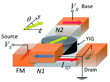
Recently, magnetic insulators have attracted attention as new materials for spintronics. The magnetization of Yttrium iron garnet (YIG), a ferrimagnetic insulator (FI) with a large band gap, can be activated thermallyUchida10 or electricallyKajiwara10 by means of the spin Hall effect (SHE) via a Pt contact and detected electrically in another Pt contact using the inverse SHE (ISHE). Spin transport at a normal metal (N)FI interface is governed by the spin-mixing conductance .Brataas00 The prediction of large for interfaces between YIG and simple metals by first-principle calculationsJia11 has been confirmed by experiments,Heinrich11 proving that the magnetization in insulators may undergo large spin-transfer torques. We therefore propose here a thin YIG film as central layer of an STT as shown in Fig. 1. Secondly, we suggest to take advantage of the recent discovery of the giant spin Hall effect in TaTant and WTung or Bi-doped CuCuBi to operate the STT, leading to further simplifications of the device design.
The - characteristics of the spin torque transistor with a YIG base as shown in Fig. 1 can be computed by magnetoelectronic circuit theory.Brataas00 We calculate source-drain currents, torques on the base magnetization created by the spin accumulations, and the differential resistance and gain as a function of the voltage ratio and device parameters.
At the interface between a monodomain ferromagnet with magnetization parallel to the unit vector and a paramagnetic metal, the charge and spin currents, and , driven by charge chemical potential difference and spin accumulation in the normal metal are linear functions of the interface conductances. The conventional conductances and for electrons with up and down spins, respectively, vanish when the ferromagnet is an insulator. The complex spin-mixing conductance governs the spin current polarized transverse to the magnetization. The conductance parameters are in units of the conductance quantum , contain (for ferromagnetic metals) bulk and interface contributions, and can be computed from first-principles.Xia10 For metallicXia10 ; Stiles12 and insulatingJia11 ferromagnets, is usually smaller than of and is disregarded below. It is convenient to introduce and , where is the total conductance and its polarization. The continuity equation for spin current and spin accumulation in N1 reads:
| (1) |
where are the spin currents flowing from the Source/Drain/Base ferromagnets into the spacer N1. and are the density of states at the Fermi level and the volume, and is the spin-flip relaxation time. Spin-flip can be disregarded in the normal metal node of small enough structures made from metals with weak spin dissipation such Al,Jedema00 Cu,Jedema01 Ag,Silver or graphene.graphene The spin-flip in the source and drain electrodes can simply be included by taking their magnetically active thickness as the smaller one of the spin-flip diffusion length and physical thickness. The electrically insulating base electrode is assumed to be thin and magnetically soft. The source-drain current has been derived earlierBauer10 in terms of and , the normal conductance and polarization of the metallic source/drain contacts and is the spin-mixing conductance of the source/drain (insulating base) contacts. depends on the base magnetization angle with respect to the -axis. The torque on the base magnetization created by the spin accumulation in the space is proportional to the transverse spin current into the base.Bauer10 We disregard effects of the Ørsted field produced by A steady state with finite exists when is exactly canceled by an external torque, either from an applied magnetic field or a current-induced torque from the top layer. We assume the same parameters for the upper and lower sections such that (see Fig. 1), where is the voltage over the upper layer. We keep the ratio between the mixing conductances of metal and insulator variable, viz. chose . The stationary state of the biased spin torque transistor is described by the angle at which the two torques on the base magnet cancel each other. then leads to the transcendental equation
| (2) |
where . With the source-drain conductance becomes
| (3) |
With increasing , strong non-linearities develop that for large polarizations lead to negative differential conductances for .
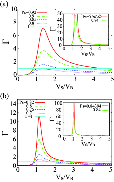
We concentrate on the differential current gain as a representative figure of merit, where is the differential transconductance and the differential source-drain conductance . While Ref. Bauer03, focused on angles , we extend the calculations of the spin torque transistor device characteristics to arbitrary working points controlled by the ratio of the applied voltages. The differential gain then reads
| (4) |
By substituting the solution of Eq. (2), we calculate the differential current gain as a function of plot it in Fig. 2 as a function of the ratio and different values of the conductance polarization of the metallic ferromagnetic contacts . The differential current gain can be huge, particularly near the half-metallic limit of , indicating that the contacts should be fabricated from high polarizations materials such as certain Heusler alloys or very thin MgO tunnel junctions. The device performance depends strongly on all parameters and is by no means universal. The critical value of for vanishing differential resistance can be computed as
| (5) | ||||
| (6) |
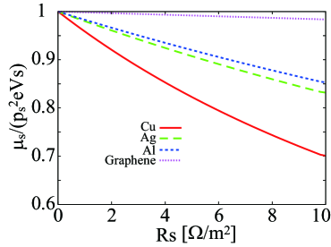
can be increased by reducing the source/drain contact areas or by introducing tunnel junctions, although this will increase the response time. It should also be kept in mind that our results are valid only when the spin accumulation is not strongly affected by spin flip assuming that . The error involved can be estimated by the spin accumulation of the spin valve for , for which the spin accumulation is limited by the spin relaxation according toSA
| (7) |
where is the bulk resistivity, the length, and the spin diffusion length. Figure 3 shows this ratio for PyCu, PyAg, PyAl, CoGraphene, using the (room temperature) parameters. and 3.0 , and 700, 600 and 2000 for Cu, Ag, Al and Graphene, respectively.Jedema03 ; Silver ; Han12
The spin Hall effect (SHE)Dyakonov10 refers to the spin current induced transverse to a charge current through a nonmagnetic material with spin-orbit interaction. Recently, large spin Hall effects have been reported in platinum,Kimura10 and CuBi alloy.CuBi -tantalum,Tant and -tungsten,Tung generate spin Hall currents large enough to induce spin-torque switching of ferromagnetic contacts. The strength of the SHE is measured by the spin Hall angle defined by the ratio, , where is the transverse spin current induced by a charge current . for Pt,Kimura10 for -Ta,Tant for -W,Tung and for CuBi alloyCuBi have been reported. We therefore suggest the device which we call the spin Hall torque transistor. In the new device, the control spin valve (upper one in Fig. 1) is replaced by a normal metal film with a large spin Hall angle. For the cited values of its performance is comparable to the one discussed above, but easier to fabricate. We point out the interest of simple bilayers of a spin Hall metal and magnetic insulator, in which an new effect has been discovered recently, viz. a dependence of the electrical resistance in the normal on the magnetization angle of the neighboring magnetic insulator, the spin Hall magnetoresistance.Nakayama13 ; Chen13 We can therefore envisage a device in which both spin valves are replaced by films of a metal with a large spin Hall angle. In this case, the steady state magnetization angle is simply . However, since the spin Hall magnetoresistance in the lower layer scales like , such a device would be not very attractive unless which has not been reported up to now. We therefore consider in the following a hybrid device consisting of a source-drain lateral spin valve as before, and only replace the upper one by a spin Hall metal.
We treat the upper layer (spin Hall system) by diffusion theory with quantum mechanical boundary conditions at the interface to the insulating magnet.Chen13 At the source-drain current into (or torque on) the magnetic insulator vanishes (is maximal) while that from the upper film is maximal (vanishes). Following Ref. Chen13, , the torque reads:
where is the film thickness, the cross section of the contact, with and the length and width of the (rectangular) wire in contact with the YIG disk, and the real part of the spin-mixing interface conductance per unit area for the top contact.
The torque-induced rotation from suppresses the spin accumulation and increases the source-drain current. As before this may lead to vanishing differential conductance. We choose a model system with and variable, but other parameters fixed, viz. . The two torques on the base magnet cancel each other, when or
| (8) |
where and
| (9) |
The enhancement factor scales with the SHE metal wire and the base magnetic insulator contact length because the spin current density is governed by the electric field The differential gain now reads
| (10) |
By substituting the solution of Eq. (8), we calculate the differential current gain as a function of and plot it in Fig, 4 for different values of the conductance polarization and the spin Hall angle .
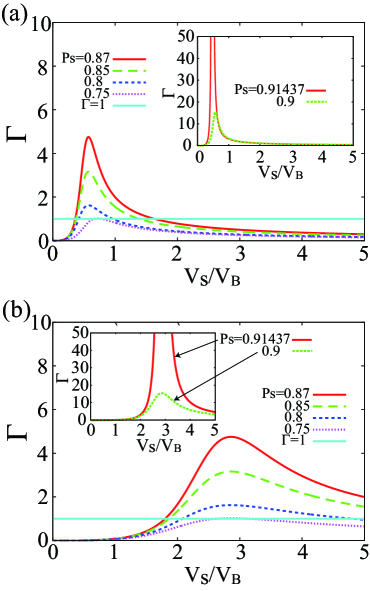
The critical value of at which in Eq. (10) becomes
| (11) | ||||
| (12) |
The spin (Hall) torque transistors can display negative differential resistance and differential gain by controlling source-drain current by the competing spin transfers on both sides of the base magnetization. We represented the negative differential resistance and gain as a function of the ratio between the base voltage and the source-drain voltage. These device can operate at room temperature, but in order to be useful, ferromagnetic materials with polarizations close to unity and normal metals with a large spin Hall angles are required. These parameters are still quite high, but might be accessible with special materials. The base contact should be a magnetic insulator in order to suppress undesired cross-talk and have a large mixing conductance with the normal metal, which is known to be the case for YIG.Jia11 ; Heinrich11 Tunnel junctions or reduced contact areas for the source-drain contacts improve the differential gain but slow down the response time and require reduced spin-flip scattering. The contact between the metals and YIG should be relatively large. Since the current-induced torques due to the spin Hall effect are comparable to that from spin valves, the performance of the spin (Hall) torque transistor can be comparable to the old type, but might be easier to fabricate. We also note that while , is not limited by any principle.
The spin torque transistors are to our knowledge the only spintronics devices that provide analogue gain; this in contrast to the Oersted field-operated digital scheme in Ref. Konishi12, (that, by the way, could also work with the spin Hall effect). A disadvantage of the spin torque transistor is the stand-by current that is analogous to the leakage current in bipolar transistors. The full electric control of the magnetization direction without need for magnetic field might find applications as well.
This work was supported by FOM (Stichting voor Fundamenteel Onderzoek der Materie), EU-ICT-7 “MACALO,” the ICC-IMR, DFG Priority Programme 1538 “Spin-Caloric Transport” (GO 944/4), and KAKENHI (No. 22540346).
References
- (1) S. Datta and B. Das, Appl. Phys. Lett. 56, 665 (1990).
- (2) K. Konishi, T. Nozaki, H. Kubota, A. Fukushima, S. Yuasa, and Y. Suzuki, IEEE Trans. Magn. 48, 1134 (2012).
- (3) G. E. W. Bauer, A. Brataas, Y. Tserkovnyak, and B. J. van Wees, Appl. Phys. Lett. 82, 3928 (2003).
- (4) K. Uchida, J. Xiao, H. Adachi, J. Ohe, S. Takahashi, J. Ieda, T. Ota, Y. Kajiwara, H. Umezawa, H. Kawai, G. E.W. Bauer, S. Maekawa, and E. Saitoh, Nature Mater. 9, 894 (2010).
- (5) Y. Kajiwara, K. Harii, S. Takahashi, J. Ohe, K. Uchida, M. Mizuguchi, H. Umezawa, H. Kawai, K. Ando, K. Takanashi, S. Maekawa, and E. Saitoh, Nature 464, 262 (2010).
- (6) A. Brataas, Yu. V. Nazarov, and G. E. W. Bauer, Phys. Rev. Lett. 84, 2481 (2000); Eur. Phys. J. B 22, 99 (2001).
- (7) X. Jia, K. Liu, K. Xia, and G. E. W. Bauer, Europhys. Lett. 96, 17005 (2011).
- (8) C. Burrowes, B. Heinrich, B. Kardasz, E. A. Montoya, E. Girt, Y. Sun, Y. Y. Song, and M. Wu, Appl. Phys. Lett. 100, 092403 (2012).
- (9) L. Liu, C.-F. Pai, Y. Li, H. W. Tseng, D. C. Ralph, R. A. Buhrman, Science 336, 555 (2012).
- (10) C.-F. Pai, L. Liu, Y. Li, H. W. Tseng, D. C. Ralph, and R. A. Buhrman, Appl. Phys. Lett. 101, 122404 (2012).
- (11) Y. Niimi, Y. Kawanishi, D. H. Wei1, C. Deranlot, H. X. Yang, M. Chshiev, T. Valet, A. Fert, and Y. Otani, Phys. Rev. Lett. 109, 156602 (2012).
- (12) K. Xia, P. J. Kelly, G. E. W. Bauer, A. Brataas, and I. Turek, Phys. Rev. B 65, 220401 (2002).
- (13) M. D. Stiles and A. Zangwill, Phys. Rev. B 66, 14407 (2002).
- (14) F. J. Jedema, H. B. Heersche, A. T. Filip, J. J. A. Baselmans, and B. J. van Wees, ibid. 416, 713 (2002); S. O. Valenzuela and M. Tinkham, Nature 442, 176 (2006).
- (15) F. J. Jedema, A. T. Filip, and B. J. van Wees, Nature (London) 410, 345 (2000).
- (16) T. Kimura and Y. Otani, Phys. Rev. Lett. 99, 196604 (2007).
- (17) M. Wojtaszek, I. J. Vera-Marun, T. Maassen, and B. J. van Wees, Phys. Rev. B 87, 081402(R) (2013)
- (18) G. E. W. Bauer, Y. Tserkovnyak, D. Huertas, and A. Brataas, Phys. Rev. B 67, 094421 (2003).
- (19) A. Brataas, Y.V. Nazarov, J. Inoue, G.E.W. Bauer, Phys. Rev. B 59, 93 (1999); Eur. Phys. J. B 9, 421 (1999).
- (20) F. J. Jedema, M. S. Nijboer, A. T. Filip, and B. J. van Wees, Phys. Rev. B 67, 085319 (2003); J. Bass and W. P. Pratt. J. Phys. Condens. Matter 19, 183201 (2007).
- (21) W. Han and R. K. Kawakami, Phys. Rev. Lett. 107, 047207 (2011); M. H. D. Guimarães, A. Veligura, P. J. Zomer, T. Maassen, I. J. Vera-Marun, N. Tombros, and B. J. van Wees, Nano Lett. 12, 3512 (2012).
- (22) M. I. Dyakonov and V. I. Perel, Phys. Lett. A 35, 459 (1971); J. E. Hirsch, Phys. Rev. Lett. 83, 1834 (1999).;S. F. Zhang, Phys. Rev. Lett. 85, 393 (2000).
- (23) T. Kimura, Y. Otani, T. Sato, S. Takahashi, and S. Maekawa, Phys. Rev. Lett. 98, 156601 (2007); K. Ando, S. Takahashi, K. Harii, K. Sasage, J. Ieda, S. Maekawa, and E. Saitoh, Phys. Rev. Lett. 101, 036601 (2008); O. Mosendz, J. E. Pearson, F. Y. Fradin, G. E. W. Bauer, S. D. Bader, and A. Hoffmann, Phys. Rev. Lett. 104, 046601 (2010); L. Q. Liu, T. Moriyama, D. C. Ralph, and R. A. Buhrman, Phys. Rev. Lett. 106, 036601 (2011); L. Q. Liu, O. J. Lee, T. D. Gudmundsen, R. A. Buhrman, and D. C. Ralph, arXiv:1110.6846; L. Q. Liu, R. A. Buhrman, and D. C. Ralph, arXiv:1111.3702.
- (24) H. Nakayama, M. Althammer, Y.-T. Chen, K. Uchida, Y. Kajiwara, D. Kikuchi, T. Ohtani, S. Geprägs, M. Opel, S. Takahashi, R. Gross, G. E. W. Bauer, S. T. B. Goennenwein, E. Saitoh, arXiv:1211.0098..
- (25) Y. Chen, S. Takahashi, H. Nakayama, M. Althammer, S. T. B. Goennenwein, E. Saitoh, G. E. W. Bauer, arXiv:1302.1352.