Local density of states study of a spin-orbit-coupling induced Mott insulator Sr2IrO4
Abstract
We present scanning tunneling microscopy and spectroscopy experiments on the novel Mott insulator Sr2IrO4. Local density of states (LDOS) measurements show an intrinsic insulating gap of 620 meV that is asymmetric about the Fermi level and is larger than previously reported values. The size of this gap suggests that Sr2IrO4 is likely a Mott rather than Slater insulator. In addition, we found a small number of native defects which create in-gap spectral weight. Atomically resolved LDOS measurements on and off the defects shows that this energy gap is quite fragile. Together the extended nature of the 5d electrons and poor screening of defects help explain the elusive nature of this gap.
pacs:
71.30.+h, 71.27.+a, 74.55.+vUnlike localized 3d electrons and their resultant Mott insulating states Zaanen et al. (1985), 4d and 5d electrons are more extended in space and thus should have both reduced on-site Coulomb repulsion (U) and enhanced energy bandwidths (W). Because of this, many 4d systems Nakatsuji and Maeno (2000); Perry et al. (2006); Martins et al. (2011) are close to the borderline (UW) of localization and one might expect that 5d systems will be metallic (UW). However, many iridium oxides Crawford et al. (1994); Cao et al. (1998); Singh and Gegenwart (2010); Okabe et al. (2011) have instead been found to be insulators. Recently, it has been shown that for octahedrally coordinated () the large spin-orbit coupling (SOC), inherent to such a heavy element (), can dominate the orbitals and split them into a doublet and a quartet Kim et al. (2008). In this strong SOC limit, the quartet band is fully occupied and the conduction band becomes the half-filled band with a much smaller W. This means that the iridium oxides can be driven across the Mott transition borderline with a much smaller U compared to 3d materials.
One of these 5d materials, , is of particular interest, since it is the first material shown to have this SOC-induced insulating state Kim et al. (2008, 2009). In addition, it bears many similarities with the well-studied Kim et al. (2012a), a parent compound of the high-Tc superconductors, leading to an appealing possibility of superconductivity in with doping Wang and Senthil (2011); Watanabe et al. (2013). However, one of the similarities to , which relies on being in the strong SOC limit so that only the band needs to be considered, becomes less certain when one realizes that the electron hopping energy ( eV Wang and Senthil (2011); Watanabe et al. (2010)) is close to the SOC energy ( eV Montalti et al. (2006)). The deviation from the strong SOC limit has been confirmed by the recent work by Haskel et al. Haskel et al. (2012) Furthermore, instead of the Mott type insulator, the magnetically originated Slater insulator has also been proposed Arita et al. (2012), partially supported by time-resolved optical measurements Hsieh et al. (2012), while more recent investigations have shown the possibility of an intermediate regime Watanabe et al. (2014).
A key to identify the nature of this insulator is to answer the important questions of what is the size of the insulating gap, , and how does it compare to other energy scales (e.g. and ). Surprisingly, measurements of the gap size from different probes in vary widely. Gaps as low as eV have been reported by fitting the resistivity data with a thermal activation model Shimura et al. (1995); Ge et al. (2011) and by calculations using local density approximation (LDA) with SOC and U Kim et al. (2008); Jin et al. (2009). On the other hand, angle-resolved photoemission spectroscopy (ARPES) measurements do not agree with this value since the maximum of the valence band is already lower than 0.1 eV Kim et al. (2008); Wang et al. . Optical conductivity and resonant inelastic x-ray scattering (RIXS) studies both yield eV Kim et al. (2008, 2012a); Moon et al. (2009). To resolve these discrepancies, it is highly desirable to measure the gap with an experiment that directly probes the free charge carriers.
We have carried out scanning tunneling microscopy (STM) and spectroscopy (STS) experiments on . Through single-particle tunneling, STS measurements cover both occupied and unoccupied states, yielding the local density of states (LDOS) to a good approximation and hence the single particle insulating gap directly Feenstra and Må rtensson (1988); Ye et al. (2013); Okada et al. (2013). Furthermore, the spatial resolution enables us to study variation down to the atomic-scale and to search for native defects that can pin the chemical potential and affect other bulk properties. In this letter, we present high quality atomically resolved topographic 111The topographic images have been processed to remove intermittent vibrational noise at 45 Hz. and spectroscopic studies in , uncovering a gap of 620 meV. We have also studied topography with various junction resistances, and measured the LDOS with respect to the defects and to the tip-sample separation. It is worth mentioning that similar STM studies have been done by other groups Nichols et al. (2014); Li et al. (2013), although the results and conclusions are not quite converging.
In this study, single-crystals of were cleaved in ultra-high vacuum (5 torr) immediately before being loaded into the STM scan-head, whose temperature is precisely stabilized at 80 K. Before the tunneling experiments, we verified that the density of states of the tips were featureless. For this data the junction was measured to have a work function of eV, which is necessary for measurements with bias voltages up to V. Due to the insulating nature of measurements with high temperature and with large junction resistance ( ) are necessary (see below) to only minimally perturb the surfaces. Furthermore, cleaves between two SrO layers leaving a charge-balanced surface, unlike the various surface terminations resulted from polar cleave such as the 122 Fe-based superconductor Zeljkovic et al. (2013).
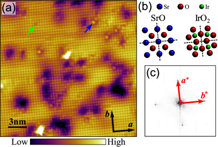
After cleaved, shows a SrO layer on the surface. Fig. 1a shows a 2020 nm2 constant-current image, in which we can easily see a square lattice (Fig. 1b). This surface lattice could be assigned as Sr, since when we partially replace Ir by Rh, the Rh dopants locate in-between four surface atoms Dai . The Fourier transform (Fig. 1c) of this image shows four atomic peaks, confirming that this high quality surface is free of reconstruction. Together with the atomic lattice, the sample also shows a small number of defects with the most evident type being the dark patches (see below).
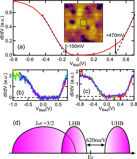
Shown in Fig. 2a is an LDOS spectrum measured by averaging 1300 spectra taken over a 22 nm2 area that did not include any apparent defects. The negative sample-bias side of the LDOS, corresponding to the occupied states, shows no distinct feature that can be related to the lower Hubbard band (LHB) of band down to 1 eV (Fig. 2b). This observation may seem to contrast with the double-peak structure observed in optical conductivity measurements Moon et al. (2009). However, these measurements in insulators are sensitive to excitons Kittel (2004) and Kim et al. Kim et al. (2012b) have pointed out that the double-peak seen in the optical conductivity are not due to the quartet band and the LHB. Additionally, in the related compounds and , the importance of excitonic effects have been shown in a recent RIXS study Gretarsson et al. (2013). It is therefore likely that the LHB is overlapping with rather than separate from the quartet band, in good agreement with calculations done by LDA+DMFT Arita et al. (2012) and by variational cluster approximation Watanabe et al. (2010). According to Watanabe et al. Watanabe et al. (2010), the LHB is entirely enclosed by the quartet band. This overlap implies that the strong SOC limit and single-band models are insufficient for . It is important to note that our data indicates that the SrO layer has little effect on the LDOS because defects like those shown by the arrows in Fig. 1a in this layer show no strong LDOS feature. In addition, any DOS contribution from this layer would give additional weight to our spectra and serve to make our gap measurement lower than the layer. While ARPES hasn’t identified the nature of all the measured bands their measurements agree that the only states within eV on the filled side of the Fermi level are from a single band in agreement with theory Wang et al. . This means that if there is a Sr band it is mixed with the ones and will not give a separate contribution to the LDOS.
The insulating gap from our tunneling spectra is about 620 meV, with the valence band top at 150 meV and conduction band bottom at +470 meV (Fig. 2a), which is much larger than the gap value reported by Li et al.Li et al. (2013) Although similar gap size has been claimed by Nichols et al. Nichols et al. (2014), their definition of the gap is quite different from ours. Here the energy gap is defined as the size of the energy window without density of states, and the edges of the gap are determined by linearly extrapolating the bands to vertical zeros 222Due to the lack of a fine modeling of the band edges and the thermal broadening at 80 K, the exact gap size could even be larger than 620 meV and the uncertainty of our measurement could be as large as 30 meV., similar to the definition used by Okada et al. in their study of Okada et al. (2013). The energy of the valence band top (150 meV) is in excellent agreement with the one measured by ARPES Kim et al. (2008); Wang et al. . The slow rise in the LDOS between 0.2 and 0.5 eV varies with tunneling location and tip-induced electric field and hence we believe it to be extrinsic either due to local defect states or variable tip-induced band bending. This extrinsic nature is further confirmed by the uniformity of the 620 meV gap unlike the slowly rising LDOS inside it which is seen only in some but not all of the locations (Figs. 2b and 2c) and at different junction resistances (Fig. 3f). The reduction of this feature with decreased tip-induced electric field is consistent with it not being the intrinsic spectrum but instead due to band bending and defect related charging. We report values for the large gap that are the limits as we lower the perturbing field. Therefore, the large 620 meV gap is due to the underlying nonlocal energy bands. Furthermore, LDOS measurements in Rh-doped sample Sr2IrRhxO4 Dai also confirm this by showing that far from the Rh sites a similarly sized gap is present.
However, as discussed above, this large gap is not in good agreement with the gap values reported by other probes. It is interesting to note that in the similar material , the debate about the gap size has lasted for a long time Uchida et al. (1991); Kim et al. (2002); Ellis et al. (2008). The difficulty in extracting the correct energy scales of the intrinsic gap rises when different types of experiments actually probe them using different processes. STS can measure the Mott gap via tunneling processes directly associated to the band edges.
Naturally, this 620 meV gap suggests that is unlikely a Slater insulator, since the magnetic coupling energy is merely 60100 meV Kim et al. (2012a); Fujiyama et al. (2012) which is too small to account for the large gap. Additionally, while the long-range magnetic ordering temperature is = 240 K, resistivity measurement does not see a metallic state up to 600 K Chikara et al. (2009) suggesting that the magnetic ordering is unlikely the source of the insulating behavior. The STS gap measurement should be further checked by experiment at temperatures above , in which a reliable measurement has yet to be established. Thus, it still possible that the magnetic ordering is playing a role in the measured gap of 620 meV, such as in the recent proposal of intermediate Mott-Slater regime Watanabe et al. (2014) or in a strong coupling mechanism.
Although the size of this gap is considerably smaller than the cuprates Ye et al. (2013); Uchida et al. (1991), it is still large compared to what one would expect from the extended 5d orbitals and the fact that , which we naively expected to have a higher U and lower W, is actually a paramagnetic Fermi liquid Perry et al. (2006); Baumberger et al. (2006). The band minimum of the upper Hubbard band (UHB) of the band, is the major discrepancy between our STS result and the existing studies. LDOS measurements show that the band minimum of UHB is at +470 meV, implying that LDA calculations need a larger U to capture this feature since it has been shown that the insulating gap depends on U sensitively Arita et al. (2012). In a recent study on , Comin et al. Comin et al. (2012) have shown that using U as large as 3 eV in LDA calculation is necessary to reproduce the 340 meV gap in that material. With this work a stronger-than-expected correlation effect has now been observed in two iridates. The measured gap in is nearly twice the measured gap seen in , indicating that in the material studied here the 5d electrons are even more correlated (larger U/W). Moreover, is also an insulator Singh and Gegenwart (2010) with a larger W due to the absence of the octahedra rotation and recent ARPES study has shown that its gap does not close above Moser et al. (2014), which further confirms the strong entanglement of the energy scales in the 5d electrons.
The spatially extended nature of the 5d electrons would seem to greatly reduce the on-site Coulomb repulsion, but will concomitantly increase the same type of interactions between the electrons sitting on neighboring Ir sites due to the increased overlap of their wave functions. This neighboring Coulomb interaction has been theoretically studied in the extended Hubbard model van den Brink et al. (1995). For , the Wannier functions calculated by Jin et al. Jin et al. (2009) do show that a significant amount of electron weight is distributed on the four neighboring sites. It is thus strongly possible that the symmetric arrangement of the neighbors can result in a net repulsion that acts as an effective on-site one. Interestingly, every ion in has four nearest neighbors while there are only three in which has a smaller gap. This is in agreement with their gap sizes if the neighboring interaction is indeed causing a larger Hubbard-U.
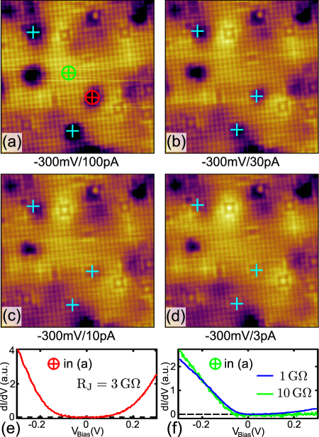
To understand the effects caused by the defects, we have further studied topography at different junction resistances and LDOS on and off the defects. We see two types of Sr-related defects in the topography: Sr vacancy (indicated by the green arrow in Fig. 1a) and Sr ad-atom (blue arrow in Fig. 1a). These two types of defects may be caused by the cleaving process, but we find they have little effect on the local electronic structure, as discussed above. In stark contrast the third type of defect we see, the larger dark patches seen in the topography, changes the local electronic structure dramatically. We identify these dark-patch defects as related to oxygen defects, similar to those seen in manganites Bryant et al. (2011) and cuprates McElroy et al. (2005); Zeljkovic et al. (2012). Topographic images (Fig. 3) with junction resistance ranging from 3.3 to 100 G confirm that the patchiness associated with these defects are due to electronic inhomogeneity rather than surface structural corrugation. The cross signs in Fig. 3a-d indicate these oxygen defect related areas that vary with different tip-sample separation. Such a high sensitivity in topography with respect to the tunneling junction reflects the poor screening in the presence of perturbations due to the insulating nature of , and also the potential influence of the defects in these materials. It is true that for some transition metal oxides, oxygen atoms in surface layers are volatile, but we didn’t observe any degradation of surface quality after several days at 80 K implying the stability of the surface and these defects. Therefore, these (O related) defects are likely native to the sample, in accord with the O deficiency found in this material Korneta et al. (2010); Qi et al. (2011), and also in and Cao . This result naturally explains why transport measurements give a smaller gap Shimura et al. (1995); Ge et al. (2011) and optical conductance shows a slow rise starting at 0.2 eV Moon et al. (2009). The presence of these defects leads to in-gap states, lowers the effective gap measured by transport and gives a lower energy scale for optical transitions. More importantly, the random distribution of the defects is in good agreement with the variable-range-hopping behavior in electrical conductivity Cao et al. (1998). The existence of native defects despite the good sample quality and our ability to measure the intrinsic LDOS apart from the influence of defects, prove the necessity of using a local probe like STM to study this material.
Lastly, the LDOS study on top of a defect (Fig. 3e) shows how strongly the tip’s electric field can change the density of states around by building up in-gap states. It should be pointed out that, due to the dramatic difference in topography of this defect as we mentioned earlier, the STS measurement may not be simply reflecting the underlying LDOS, but it does serve as evidence for the in-gap states around them. Fig. 3f shows the subtle variation in the measured spectra related to the tip-induced band bending, reinforcing the necessity of measuring with high junction resistances to reduce the perturbing electric field of the tip.
In summary, we have presented a high quality atomic-scale study in with density of states measurement covering the entire Mott gap, which is 620 meV. The measurement of the occupied states has confirmed the overlap between LHB and quartet band. We suggest that is a Mott but not Slater insulator after comparing the gap size with the magnetic coupling energy, implying the stronger-than-expected el-el correlation in this 5d system. Furthermore, we propose that additional source of Coulomb repulsion needs to be taken into account to model the 5d electron systems. Lastly, the junction dependence of the defects in the topography, combined with the LDOS results around them, indicate their profound impacts on the local electronic structure of this insulator. Our results imply that in the three energy scales (SOC, U and W) are comparable to each other and that studies of the 5d electrons should put all of them on similar-footing.
Acknowledgements.
Thanks to Michael Hermele, Gang Chen, Yue Cao and Dan Dessau for useful discussions. G.C. acknowledges support by NSF through grants DMR-0856234 and EPS-0814194. K.M. acknowledges support by Alfred P. Sloan foundation.References
- Zaanen et al. (1985) J. Zaanen, G. Sawatzky, and J. Allen, Phys. Rev. Lett. 55, 418 (1985).
- Nakatsuji and Maeno (2000) S. Nakatsuji and Y. Maeno, Phys. Rev. Lett. 84, 2666 (2000).
- Perry et al. (2006) R. S. Perry, F. Baumberger, L. Balicas, N. Kikugawa, N. J. C. Ingle, A. Rost, J. F. Mercure, Y. Maeno, Z. X. Shen, and A. P. Mackenzie, New J. Phys. 8, 175 (2006).
- Martins et al. (2011) C. Martins, M. Aichhorn, L. Vaugier, and S. Biermann, Phys. Rev. Lett. 107, 266404 (2011).
- Crawford et al. (1994) M. Crawford, M. Subramanian, R. Harlow, J. Fernandez-Baca, Z. Wang, and D. Johnston, Phys. Rev. B 49, 9198 (1994).
- Cao et al. (1998) G. Cao, J. Bolivar, S. McCall, J. Crow, and R. Guertin, Phys. Rev. B 57, R11039 (1998).
- Singh and Gegenwart (2010) Y. Singh and P. Gegenwart, Phys. Rev. B 82, 064412 (2010).
- Okabe et al. (2011) H. Okabe, M. Isobe, E. Takayama-Muromachi, A. Koda, S. Takeshita, M. Hiraishi, M. Miyazaki, R. Kadono, Y. Miyake, and J. Akimitsu, Phys. Rev. B 83, 155118 (2011).
- Kim et al. (2008) B. Kim, H. Jin, S. Moon, J. Kim, B. Park, C. Leem, J. Yu, T. Noh, C. Kim, S. Oh, J. Park, V. Durairaj, G. Cao, and E. Rotenberg, Phys. Rev. Lett. 101, 076402 (2008).
- Kim et al. (2009) B. J. Kim, H. Ohsumi, T. Komesu, S. Sakai, T. Morita, H. Takagi, and T. Arima, Science 323, 1329 (2009).
- Kim et al. (2012a) J. Kim, D. Casa, M. Upton, T. Gog, Y. Kim, J. Mitchell, M. VanVeenendaal, M. Daghofer, J. VandenBrink, G. Khaliullin, and B. Kim, Phys. Rev. Lett. 108, 177003 (2012a).
- Wang and Senthil (2011) F. Wang and T. Senthil, Phys. Rev. Lett. 106, 136402 (2011).
- Watanabe et al. (2013) H. Watanabe, T. Shirakawa, and S. Yunoki, Phys. Rev. Lett. 110, 027002 (2013).
- Watanabe et al. (2010) H. Watanabe, T. Shirakawa, and S. Yunoki, Phys. Rev. Lett. 105, 216410 (2010).
- Montalti et al. (2006) M. Montalti, A. Credi, L. Prodi, and M. T. Gandolfi, Handbook of Photochemistry, Third Edition (CRC Press, 2006).
- Haskel et al. (2012) D. Haskel, G. Fabbris, M. Zhernenkov, P. Kong, C. Jin, G. Cao, and M. VanVeenendaal, Phys. Rev. Lett. 109, 027204 (2012).
- Arita et al. (2012) R. Arita, J. Kunes, A. Kozhevnikov, A. Eguiluz, and M. Imada, Phys. Rev. Lett. 108, 086403 (2012).
- Hsieh et al. (2012) D. Hsieh, F. Mahmood, D. Torchinsky, G. Cao, and N. Gedik, Phys. Rev. B 86, 035128 (2012).
- Watanabe et al. (2014) H. Watanabe, T. Shirakawa, and S. Yunoki, Phys. Rev. B 89, 165115 (2014).
- Shimura et al. (1995) T. Shimura, Y. Inaguma, T. Nakamura, M. Itoh, and Y. Morii, Phys. Rev. B 52, 9143 (1995).
- Ge et al. (2011) M. Ge, T. Qi, O. Korneta, D. DeLong, P. Schlottmann, W. Crummett, and G. Cao, Phys. Rev. B 84, 100402 (2011).
- Jin et al. (2009) H. Jin, H. Jeong, T. Ozaki, and J. Yu, Phys. Rev. B 80, 075112 (2009).
- (23) Q. Wang, Y. Cao, J. A. Waugh, S. R. Park, T. F. Qi, O. B. Korneta, G. Cao, and D. S. Dessau, arXiv:1210.4141 .
- Moon et al. (2009) S. Moon, H. Jin, W. Choi, J. Lee, S. Seo, J. Yu, G. Cao, T. Noh, and Y. Lee, Phys. Rev. B 80, 195110 (2009).
- Feenstra and Må rtensson (1988) R. Feenstra and P. Må rtensson, Phys. Rev. Lett. 61, 447 (1988).
- Ye et al. (2013) C. Ye, P. Cai, R. Yu, X. Zhou, W. Ruan, Q. Liu, C. Jin, and Y. Wang, Nat. Commun. 4, 1365 (2013).
- Okada et al. (2013) Y. Okada, D. Walkup, H. Lin, C. Dhital, T.-R. Chang, S. Khadka, W. Zhou, H.-T. Jeng, M. Paranjape, A. Bansil, Z. Wang, S. D. Wilson, and V. Madhavan, Nature Mater. (2013), 10.1038/nmat3653.
- Note (1) The topographic images have been processed to remove intermittent vibrational noise at 45 Hz.
- Nichols et al. (2014) J. Nichols, N. Bray-Ali, A. Ansary, G. Cao, and K.-W. Ng, Phys. Rev. B 89, 085125 (2014).
- Li et al. (2013) Q. Li, G. Cao, S. Okamoto, J. Yi, W. Lin, B. C. Sales, J. Yan, R. Arita, J. Kuneš, A. V. Kozhevnikov, A. G. Eguiluz, M. Imada, Z. Gai, M. Pan, and D. G. Mandrus, Sci. Rep. 3, 3073 (2013).
- Zeljkovic et al. (2013) I. Zeljkovic, D. Huang, C.-L. Song, B. Lv, C.-W. Chu, and J. E. Hoffman, Phys. Rev. B 87, 201108 (2013).
- (32) J. Dai, (unpublished).
- Kittel (2004) C. Kittel, Introduction to Solid State Physics (John Wiley & Sons, 2004).
- Kim et al. (2012b) B. Kim, G. Khaliullin, and B. Min, Phys. Rev. Lett. 109, 167205 (2012b).
- Gretarsson et al. (2013) H. Gretarsson, J. P. Clancy, X. Liu, J. P. Hill, E. Bozin, Y. Singh, S. Manni, P. Gegenwart, J. Kim, A. H. Said, D. Casa, T. Gog, M. H. Upton, H.-S. Kim, J. Yu, V. M. Katukuri, L. Hozoi, J. van den Brink, and Y.-J. Kim, Phys. Rev. Lett. 110, 076402 (2013).
- Note (2) Due to the lack of a fine modeling of the band edges and the thermal broadening at 80 K, the exact gap size could even be larger than 620 meV and the uncertainty of our measurement could be as large as 30 meV.
- Uchida et al. (1991) S. Uchida, T. Ido, H. Takagi, T. Arima, Y. Tokura, and S. Tajima, Phys. Rev. B 43, 7942 (1991).
- Kim et al. (2002) Y. Kim, J. Hill, C. Burns, S. Wakimoto, R. Birgeneau, D. Casa, T. Gog, and C. Venkataraman, Phys. Rev. Lett. 89, 177003 (2002).
- Ellis et al. (2008) D. Ellis, J. Hill, S. Wakimoto, R. Birgeneau, D. Casa, T. Gog, and Y. Kim, Phys. Rev. B 77, 060501 (2008).
- Fujiyama et al. (2012) S. Fujiyama, H. Ohsumi, T. Komesu, J. Matsuno, B. Kim, M. Takata, T. Arima, and H. Takagi, Phys. Rev. Lett. 108, 247212 (2012).
- Chikara et al. (2009) S. Chikara, O. Korneta, W. Crummett, L. DeLong, P. Schlottmann, and G. Cao, Phys. Rev. B 80, 140407 (2009).
- Baumberger et al. (2006) F. Baumberger, N. Ingle, W. Meevasana, K. Shen, D. Lu, R. Perry, A. Mackenzie, Z. Hussain, D. Singh, and Z. Shen, Phys. Rev. Lett. 96, 246402 (2006).
- Comin et al. (2012) R. Comin, G. Levy, B. Ludbrook, Z. Zhu, C. Veenstra, J. Rosen, Y. Singh, P. Gegenwart, D. Stricker, J. Hancock, D. VanderMarel, I. Elfimov, and A. Damascelli, Phys. Rev. Lett. 109, 266406 (2012).
- Moser et al. (2014) S. Moser, L. Moreschini, A. Ebrahimi, B. Dalla Piazza, M. Isobe, H. Okabe, J. Akimitsu, V. V. Mazurenko, K. S. Kim, A. Bostwick, E. Rotenberg, J. Chang, H. M. Rø nnow, and M. Grioni, New J. Phys. 16, 013008 (2014).
- van den Brink et al. (1995) J. van den Brink, M. Meinders, J. Lorenzana, R. Eder, and G. Sawatzky, Phys. Rev. Lett. 75, 4658 (1995).
- Bryant et al. (2011) B. Bryant, C. Renner, Y. Tokunaga, Y. Tokura, and G. Aeppli, Nat. Commun. 2, 212 (2011).
- McElroy et al. (2005) K. McElroy, J. Lee, J. A. Slezak, D.-H. Lee, H. Eisaki, S. Uchida, and J. C. Davis, Science 309, 1048 (2005).
- Zeljkovic et al. (2012) I. Zeljkovic, Z. Xu, J. Wen, G. Gu, R. S. Markiewicz, and J. E. Hoffman, Science 337, 320 (2012).
- Korneta et al. (2010) O. Korneta, T. Qi, S. Chikara, S. Parkin, L. DeLong, P. Schlottmann, and G. Cao, Phys. Rev. B 82, 115117 (2010).
- Qi et al. (2011) T. F. Qi, O. B. Korneta, S. Chikara, M. Ge, S. Parkin, L. E. De Long, P. Schlottmann, and G. Cao, J. App. Phys. 109, 07D906 (2011).
- (51) G. Cao, (unpublished).