Valley-Spin Polarization in the Magneto-Optical Response of Silicene and Other Similar 2D Crystals
Abstract
We calculate the magneto-optical conductivity and electronic density of states for silicene, the silicon equivalent of graphene, and similar crystals such as germanene. In the presence of a perpendicular magnetic field and electric field gating, we note that four spin- and valley-polarized levels can be seen in the density of states and transitions between these levels lead to similarly polarized absorption lines in the longitudinal, transverse Hall, and circularly polarized dynamic conductivity. While previous spin and valley-polarization predicted for the conductivity is only present in the response to circularly polarized light, we show that distinct spin- and valley-polarization can also be seen in the longitudinal magneto-optical conductivity at experimentally attainable energies. The frequency of the absorption lines may be tuned by the electric and magnetic field to onset in a range varying from THz to the infrared. This potential to isolate charge carriers of definite spin and valley label may make silicene a promising candidate for spin- and valleytronic devices.
pacs:
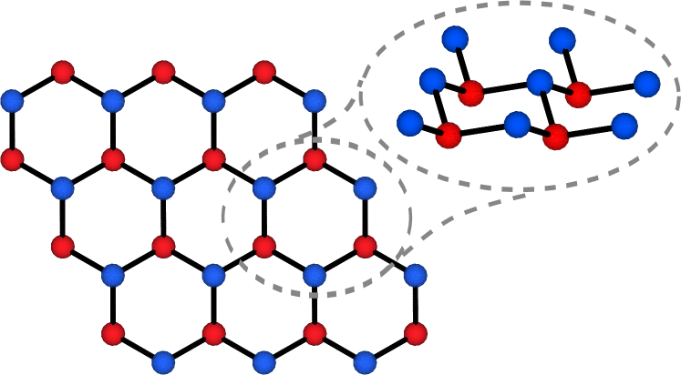
78.67.Wj, 78.20.Ls, 71.70.Di, 72.80.VpIntroduction: Silicene, a monolayer of silicon atoms bonded together on a two-dimensional (2D) honeycomb lattice, has recently been synthesizedLalmi et al. (2010); De Padova et al. (2010, 2011); Vogt et al. (2012); Lin et al. (2012); Fleurence et al. (2012) and begun to garner increased theoretical attentionGuzmán-Verri and Lew Yan Voon (2007); Topsakal and Ciraci (2010); Liu et al. (2011a, b); Ni et al. (2012); Drummond et al. (2012); Ezawa (2012a, b, c); Stille et al. (2012); Ezawa (2013); Tahir and Schwingenschlögl (2013) as it features a Dirac-like electron dispersion at the points of the Brillouin zone and promises to exhibit exciting properties beyond those present in graphene. The similarities with graphene result from carbon and silicon residing in the same column on the chemical periodic table. The larger ionic size of silicon atoms causes the 2D lattice of silicene to be buckledLiu et al. (2011a, b); Drummond et al. (2012) such that sites on the A and B sublattices sit in different vertical planes with a separation of ÅNi et al. (2012); Drummond et al. (2012) as illustrated in Fig. 1.
Because of the buckled lattice, an onsite potential difference () arises between the A and B sublattices when an electric field is applied perpendicular to the plane. Silicene is also predicted to have a stronger intrinsic spin-orbit gap than is seen in grapheneKonschuh et al. (2010) with values (which can be increased under strainLiu et al. (2011a, b)) predicted to be meV by density functional theory calculationsLiu et al. (2011a, b); Drummond et al. (2012) and is quoted as meV in tight-binding calculationsLiu et al. (2011b). The larger spin-orbit interaction makes silicene susceptible to spin manipulation. The resulting band gap near the two valleys and of the first Brillouin zone provides a “mass” to the Dirac electrons that can be controlled by the strength of Ni et al. (2012); Drummond et al. (2012); Ezawa (2012b). Silicene has also been predictedDrummond et al. (2012); Ezawa (2012b) to undergo a transition from a topological insulator (TI) (an insulator with a gapless spectrum of edge statesKane and Mele (2005); Hasan and Kane (2010)) to a band insulator (BI) as the strength of becomes greater than . These qualities are also predicted for a monolayer of germanene which is isostructural to silicene but is expected to exhibit a much stronger spin-orbit band gap of meV from first principlesLiu et al. (2011a) and tight-binding calculationsLiu et al. (2011b).
When subjected to an external magnetic field, Landau levels (LLs) form in the electronic density of states and transitions between these levels result in absorption lines in the optical conductivity. This has been discussed theoreticallyGusynin et al. (2007a, b); Pound et al. (2012) and confirmed experimentallySadowski et al. (2006, 2007); Jiang et al. (2007); Deacon et al. (2007); Plochocka et al. (2008); Orlita and Potemski (2010); Henriksen et al. (2010); Orlita et al. (2011) for graphene. In graphene, the LL is pinned at .Semenoff (1984); Gusynin et al. (2007b, a); Semenoff and Zhou (2011); Pound et al. (2012, 2011a, 2011b) When an excitonic gap is includedGusynin et al. (2007b, a), the level splits between two distinct valley-polarized spin-degenerate energies but spin-polarized charge carriers are not expected in this case. Conversely, due to spin-orbit coupling (SOC) and the response of silicene to an external perpendicular electric field, spin- and valley-polarized charge carriers appear due to the LL splitting between four spin and valley distinct energies.
In this Letter, we examine the effect of exposing silicene (or similar 2D crystals, such as germaneneLiu et al. (2011b)) to both external magnetic and electric fields with particular attention to the valley- and spin-polarized regions of the electronic density of states and dynamical conductivity. This is of particular technological interest as four distinct valley- and spin-polarized currents can be generated through use of an in-plane electric field to generate a Hall current of spin- or valley-selected charges on the edges of the sampleXiao et al. (2012); Tsai et al. (2013). This ability to control the spin and valley index for use in such applications as data storage and data transmission is integral to valley-Xiao et al. (2012); Zeng et al. (2012); Mak et al. (2012); Cao et al. (2012) and spintronicWolf et al. (2001); Fabian et al. (2007) devices.
Low Energy Hamiltonian: It has been shown that the low-energy physics of silicene can be captured by the simple low-energy HamiltonianLiu et al. (2011b); Ezawa (2012a, b, c)
| (1) |
where at the and points, respectively, is the Pauli matrix associated with the electron’s spin, are the Pauli matrices associated with the sublattice pseudospin, m/s is the Fermi velocity of silicene and and are components of the momentum measured relative to the point. The first term of the Hamiltonian is the familiar graphene-type Dirac HamiltonianCastro Neto et al. (2009); Abergel et al. (2010). The second term is the Kane-Mele term for intrinsic SOCKane and Mele (2005) while the final term is associated with the onsite potential difference between the two sublattices that results from an external electric fieldEzawa (2012a, b, c). There is also a Rashba SOC but it may be ignoredEzawa (2012a) for our purpose as it is a factor of 10 smaller than the intrinsic SOC.
If we consider a perpendicular magnetic field and work in the Landau gauge, the magnetic vector potential, , is written as . We make the Peierls substitution in Eq. (1) and obtain the low energy dispersion
| (2) |
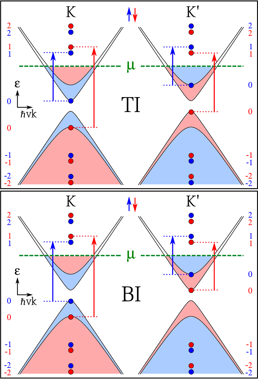
where , for spin up and down, respectively, is the elementary charge and is the strength of the external magnetic field. The Zeeman energy is small and can be ignoredTahir and Schwingenschlögl (2012); Ezawa (2012a, b, c). In Fig. 2 we show a schematic of the spin split bands at the and point for with the LLs for finite shown as dots. The form of the zeroth LL has strong implications when considering the LLs in the TI () vs. BI () regimes which can be seen in the upper frame (TI) and lower frame (BI) of Fig. 2, respectively. Given our expression for , we can see that at both points in the TI regime, the spin up LL is at positive energy while the spin down level is at negative energy; refer to the upper frame of Fig. 2. In the BI regime, is now greater than and, therefore, the signs of and switch so that the spin up level is below zero at the point while the spin down level is above zero at the point as illustrated in the lower frame of Fig. 2. This LL shift arises from the band inversion that results from the transition between the TI and BI regimesEzawa (2012b).
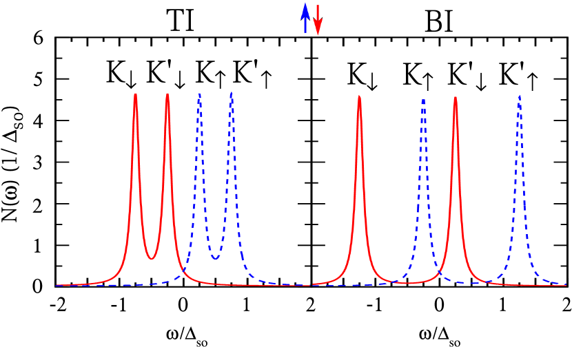
Electronic Density of States: Plots of the single-spin electronic density of states in the TI and BI regimes are shown in Fig. 3. There are four spin-polarized peaks which onset at , , and corresponding to the four LLs. The remaining higher energy peaks (not shown) are spin degenerate. As scanning tunnelling spectroscopy experiments have been successful in observing LLs in grapheneLi and Andrei (2007); Miller et al. (2009); Andrei et al. (2012), similar work on silicene should detect four distinct low energy spin- and valley-polarized levels.
Dynamical Conductivity: Using the standard Kubo formulaNicol and Carbotte (2008); Tse and MacDonald (2011); Tabert and Nicol (2012); Stille et al. (2012); Tabert and Nicol (2013), we can derive expressions for the longitudinal and transverse Hall dynamical conductivities which also yield the familiar selection rulesGusynin et al. (2007b, a); Tse and MacDonald (2011) for LL transitions. For the absorptive part of the longitudinal conductivity we find
| (3) |
where is the universal background conductivity of graphene. For the absorptive imaginary part of the transverse Hall conductivity we find
| (4) |
where
| (5) |
and
| (6) |
The absorptive part of the longitudinal conductivity can be seen in Figs. 4(a) and 4(b) for the TI and BI regimes, respectively. The transverse Hall conductivity is not shown as in the region of spin and valley polarization it is simply the negative of the longitudinal conductivity. We have used the same parameters as before and included a chemical potential of so that the Fermi level lies above all the LLs and below all the levels. This is done so that all the LLs are occupied and, thus, transitions from to are forbidden due to the Pauli exclusion principle while all to 1 transitions are permitted. This will occur for any value of that is in this region, i.e. . The lower limit, , is governed by the strength of the electric field while the upper bound, , can be raised by increasing and/or .
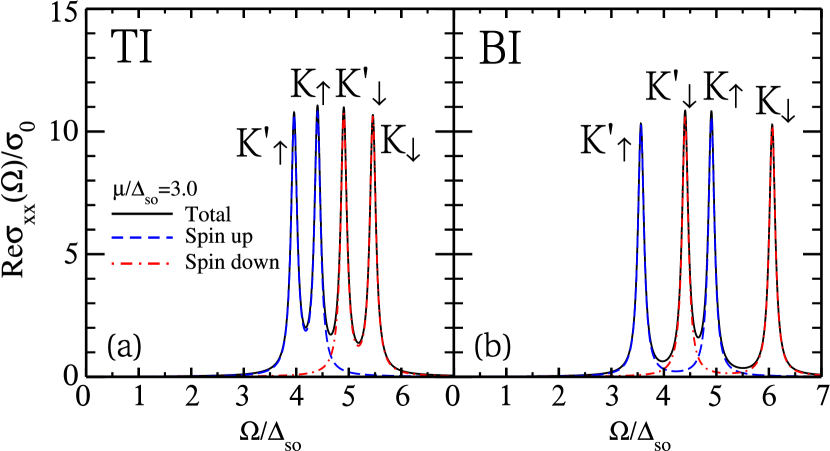
If the chemical potential is situated between and , we see four absorptive peaks in the longitudinal conductivity which are spin and valley polarized. These peaks result from single spin and valley transitions as illustrated by the arrows in Fig. 2. While in the absence of a magnetic field spin-valley polarization has been predicted in the absorptive response to circularly polarized lightEzawa (2012c); Stille et al. (2012), the inclusion of a finite produces four strong, separated peaks of definite spin and valley label which can also be observed in the longitudinal response. This is to be contrasted with the response to circularly polarized light where predicted valley-spin polarization is not clearly separated but contains some admixture of spins and valleysStille et al. (2012); Li and Carbotte (2012). Similar to the result, spin and valley polarization can be seen in the response to circularly polarized light for . Figure 5 shows the absorptive part of , where for right- and left-handed polarization, respectivelyPound et al. (2012).

There remains a spin- and valley-polarized quartet of peaks (of double weight) in response to right-handed polarization, while the quartet is lost in response to left-handed polarization and all that remains is the spin- and valley-degenerate response at higher energy. In both the longitudinal and circularly polarized responses, the two middle peaks of the quartet display a band inversionEzawa (2012b) with the transition from TI to BI regimes.
The magnetic field also allows for a tuning of the position of the valley-spin polarized peaks over a frequency range without having to adjust . The onset frequencies of these peaks is set by the energy difference between and 1 LLs, namely, , , and associated with spin up and down at and spin up and down at , respectively. Thus, as depends on , increasing the magnetic field moves the quartet of peaks to higher energy. While the separation between all four peaks is not fixed, the separation between the two middle peaks is fixed at for (all levels are spin degenerate when ) and as a consequence, when , only the outer peaks of the quartet remain spin-valley polarized. This separation is the minimum gap between the bands and is only controlled by and the SOC.
These polarized peaks should be visible in experiment as the magnetic and electric field values required to observe them are well within experimental limits. Aside from and , the determining factor in the onset frequency of the polarized response is the size of the spin orbit gap, . For meV, the curves shown here correspond to a of T and for , T. In the former case, the splitting of peaks in the polarized quartet is meV, a resolution easily achieved in broadband optics. In this case, the quartet sits in the range of THz where broad band experiments can be doneMori et al. (2008). If T, such peaks will shift to the far infrared in the range of meV. If instead is as large as 8 meV, the splitting of the quartet will be about 3-5 meV for T and the quartet will fall in the range of meV. Conductivity experiments on graphene have spanned the range from THz to eVSadowski et al. (2006, 2007); Jiang et al. (2007); Deacon et al. (2007); Henriksen et al. (2010); Crassee et al. (2011) with B T to 18 TSadowski et al. (2006, 2007); Jiang et al. (2007); Deacon et al. (2007); Henriksen et al. (2010); Crassee et al. (2011) and resolutions of order less than a meV; therefore, experiments on silicene should observe this polarized behaviour. Experiments may also provide a measure of , for instance, by examining when the two middle polarized peaks become superimposed at the transition between the TI and BI regimes ().
While electron-electron interactions have been a source of much discussion in grapheneKotov et al. (2012); Goerbig (2011), experimental magneto-optics in graphene has been well-described by the single-particle picture up to very large magnetic fields of 16TSadowski et al. (2006, 2007); Jiang et al. (2007); Deacon et al. (2007); Plochocka et al. (2008); Orlita and Potemski (2010); Goerbig (2011), hence for modest magnetic fields (1T), electron-electron interactions should not modify our main results. In addition, our calculations have been based on the assumption of freestanding silicene or silicene on an insulating substrate where the main effect is to provide charge doping, for example, by back gating. Currently silicene is fabricated on Ag substrates, but efforts are underway to find alternative substrates, most recentlyFleurence et al. (2012), ZrB2. As in graphene, the choice of insulating substrate is not expected to affect qualitatively the results presented here.
Summary: We have predicted the presence of a quartet of spin- and valley-polarized peaks in the low energy electronic density of states which result in spin- and valley-polarized absorption lines in the magneto-optical longitudinal and transverse Hall dynamical conductivities of silicene as well as in the response to circularly polarized light. These absorption peaks arise from transitions between and 1 LLs at both valleys and are only present when the chemical potential lies between the and 1 LLs at the point. The energy at which these peaks occur can be controlled by the strength of the magnetic and electric fields. Furthermore, the spin and valley labels of the two middle peaks switch as the system transitions from a TI to a BI. As the strength of the spin- and valley-polarized response is predicted to be comparable to what has been observed for graphene and to onset at experimentally attainable energies, it should be easily visible in experiment. While spin-valley polarization in the absence of a magnetic field has been discussedEzawa (2012c); Stille et al. (2012), it can only be isolated with circularly polarized light and may contain some admixture of spin and valley. With a finite , such spin-valley polarization is robust, easily separated out and can be observed without circular polarization. This may prove useful in both spintronic and valleytronic technologies as an electronic current of definite spin and valley label can potentially be isolated. These predictions should hold for other 2D crystals with a band gap that can be tuned by an external electric field (i.e. germanene).
We thank J. P. Carbotte for helpful discussions. This work has been supported by the Natural Science and Engineering Research Council of Canada.
References
- Lalmi et al. (2010) B. Lalmi, H. Oughaddou, H. Enriquez, A. Kara, S. Vizzini, B. Ealet, and B. Aufray, Appl. Phys. Lett. 97, 223109 (2010).
- De Padova et al. (2010) P. De Padova, C. Quaresima, C. Ottaviani, P. M. Sheverdyaeva, P. Moras, C. Carbone, D. Topwal, B. Olivieri, A. Kara, H. Oughaddou, B. Aufray, and G. Le Lay, Appl. Phys. Lett. 96, 261905 (2010).
- De Padova et al. (2011) P. De Padova, C. Quaresima, B. Olivieri, P. Perfetti, and G. Le Lay, Appl. Phys. Lett. 98, 081909 (2011).
- Vogt et al. (2012) P. Vogt, P. De Padova, C. Quaresima, J. Avila, E. Frantzeskakis, M. C. Asensio, A. Resta, B. Ealet, and G. Le Lay, Phys. Rev. Lett. 108, 155501 (2012).
- Lin et al. (2012) C.-L. Lin, R. Arafune, K. Kawahara, N. Tsukahara, E. Minamitani, Y. Kim, N. Takagi, and M. Kawai, Appl. Phys. Express 5, 045802 (2012).
- Fleurence et al. (2012) A. Fleurence, R. Friedlein, T. Ozaki, H. Kawai, Y. Wang, and Y. Yamada-Takamura, Phys. Rev. Lett. 108, 245501 (2012).
- Guzmán-Verri and Lew Yan Voon (2007) G. G. Guzmán-Verri and L. C. Lew Yan Voon, Phys. Rev. B 76, 075131 (2007).
- Topsakal and Ciraci (2010) M. Topsakal and S. Ciraci, Phys. Rev. B 81, 024107 (2010).
- Liu et al. (2011a) C.-C. Liu, W. Feng, and Y. Yao, Phys. Rev. Lett. 107, 076802 (2011a).
- Liu et al. (2011b) C.-C. Liu, H. Jiang, and Y. Yao, Phys. Rev. B 84, 195430 (2011b).
- Ni et al. (2012) Z. Ni, Q. Liu, K. Tang, J. Zheng, J. Zhou, R. Qin, Z. Gao, D. Yu, and J. Lu, Nano Lett. 12, 113 (2012).
- Drummond et al. (2012) N. D. Drummond, V. Zólyomi, and V. I. Fal’ko, Phys. Rev. B 85, 075423 (2012).
- Ezawa (2012a) M. Ezawa, Phys. Rev. Lett. 109, 055502 (2012a).
- Ezawa (2012b) M. Ezawa, New J. Phys. 14, 033003 (2012b).
- Ezawa (2012c) M. Ezawa, Phys. Rev. B 86, 161407(R) (2012c).
- Stille et al. (2012) L. Stille, C. J. Tabert, and E. J. Nicol, Phys. Rev. B 86, 195405 (2012).
- Ezawa (2013) M. Ezawa, Phys. Rev. Lett. 110, 026603 (2013).
- Tahir and Schwingenschlögl (2013) M. Tahir and U. Schwingenschlögl, Scientific Reports 3, 1075 (2013).
- [Crystal structure plotted using VESTA] et al. (2011) [Crystal structure plotted using VESTA], K. Momma, and F. Izumi, J. Appl. Crystallogr. 44, 1272 (2011).
- Konschuh et al. (2010) S. Konschuh, M. Gmitra, and J. Fabian, Phys. Rev. B 82, 245412 (2010).
- Kane and Mele (2005) C. L. Kane and E. J. Mele, Phys. Rev. Lett. 95, 226801 (2005).
- Hasan and Kane (2010) M. Z. Hasan and C. L. Kane, Rev. Mod. Phys. 82, 3045 (2010).
- Gusynin et al. (2007a) V. P. Gusynin, S. G. Sharapov, and J. P. Carbotte, J. Phys.: Condens. Matter 19, 026222 (2007a).
- Gusynin et al. (2007b) V. P. Gusynin, S. G. Sharapov, and J. P. Carbotte, Phys. Rev. Lett. 98, 157402 (2007b).
- Pound et al. (2012) A. Pound, J. P. Carbotte, and E. J. Nicol, Phys. Rev. B 85, 125422 (2012).
- Sadowski et al. (2006) M. L. Sadowski, G. Martinez, M. Potemski, C. Berger, and W. A. de Heer, Phys. Rev. Lett. 97, 266405 (2006).
- Sadowski et al. (2007) M. L. Sadowski, G. Martinez, M. Potemski, C. Berger, and W. A. de Heer, Solid State Commun. 143, 123 (2007).
- Jiang et al. (2007) Z. Jiang, E. A. Henriksen, L. C. Tung, Y.-J. Wang, M. E. Schwartz, M. Y. Han, P. Kim, and H. L. Stormer, Phys. Rev. Lett. 98, 197403 (2007).
- Deacon et al. (2007) R. S. Deacon, K.-C. Chuang, R. J. Nicholas, K. S. Novoselov, and A. K. Geim, Phys. Rev. B 76, 081406 (2007).
- Plochocka et al. (2008) P. Plochocka, C. Faugeras, M. Orlita, M. L. Sadowski, G. Martinez, M. Potemski, M. O. Goerbig, J.-N. Fuchs, C. Berger, and W. A. de Heer, Phys. Rev. Lett. 100, 087401 (2008).
- Orlita and Potemski (2010) M. Orlita and M. Potemski, Semicond. Sci. Technol. 25, 063001 (2010).
- Henriksen et al. (2010) E. A. Henriksen, P. Cadden-Zimansky, Z. Jiang, Z. Q. Li, L.-C. Tung, M. E. Schwartz, M. Takita, Y.-J. Wang, P. Kim, and H. L. Stormer, Phys. Rev. Lett. 104, 067404 (2010).
- Orlita et al. (2011) M. Orlita, C. Faugeras, R. Grill, A. Wysmolek, W. Strupinski, C. Berger, W. A. de Heer, G. Martinez, and M. Potemski, Phys. Rev. Lett. 107, 216603 (2011).
- Semenoff (1984) G. W. Semenoff, Phys. Rev. Lett. 53, 2449 (1984).
- Semenoff and Zhou (2011) G. Semenoff and F. Zhou, J. High Energy Phys. 2011, 1 (2011).
- Pound et al. (2011a) A. Pound, J. P. Carbotte, and E. J. Nicol, Phys. Rev. B 84, 085125 (2011a).
- Pound et al. (2011b) A. Pound, J. P. Carbotte, and E. J. Nicol, Europhys. Lett. 94, 57006 (2011b).
- Xiao et al. (2012) D. Xiao, G. B. Liu, W. Feng, X. Xu, and W. Yao, Phys. Rev. Lett. 108, 196802 (2012).
- Tsai et al. (2013) W.-F. Tsai, C.-Y. Huang, T.-R. Chang, H. Lin, H.-T. Jeng, and A. Bansil, Nature Commun. 4, 1500 (2013).
- Zeng et al. (2012) H. Zeng, J. Dai, W. Yao, D. Xiao, and X. Cui, Nature Nano. 7, 490 (2012).
- Mak et al. (2012) K. F. Mak, K. He, J. Shan, and T. F. Heinz, Nature Nano. 7, 494 (2012).
- Cao et al. (2012) T. Cao, G. Wang, W. Han, H. Ye, C. Zhu, J. Shi, Q. Niu, P. Tan, E. Wang, B. Liu, and J. Feng, Nature Commun. 3, 887 (2012).
- Wolf et al. (2001) S. A. Wolf, D. D. Awschalom, R. A. Buhrman, J. M. Daughton, S. von Molnar, M. L. Roukes, A. Y. Chtchelkanova, and D. M. Treger, Science 294, 1488 (2001).
- Fabian et al. (2007) J. Fabian, A. Matos-Abiague, C. Ertler, P. Stano, and I. Zutic, Acta Physica Slovaca 57, No.4,5 565 (2007).
- Castro Neto et al. (2009) A. H. Castro Neto, F. Guinea, N. M. R. Peres, K. S. Novoselov, and A. K. Geim, Rev. Mod. Phys. 81, 109 (2009).
- Abergel et al. (2010) D. S. L. Abergel, V. Apalkov, J. Berashevich, K. Ziegler, and T. Chakraborty, Adv. in Phys. 59, 261 (2010).
- Tahir and Schwingenschlögl (2012) M. Tahir and U. Schwingenschlögl, Appl. Phys. Lett. 101, 132412 (2012).
- Li and Andrei (2007) G. Li and E. Y. Andrei, Nature Phys. 3, 623 (2007).
- Miller et al. (2009) D. L. Miller, K. D. Kubista, G. M. Rutter, M. Ruan, W. A. de Heer, P. N. First, and J. A. Stroscio, Science 324, 924 (2009).
- Andrei et al. (2012) E. Y. Andrei, G. Li, and X. Du, Rep. Prog. Phys. 75, 056501 (2012).
- Nicol and Carbotte (2008) E. J. Nicol and J. P. Carbotte, Phys. Rev. B 77, 155409 (2008).
- Tse and MacDonald (2011) W.-K. Tse and A. H. MacDonald, Phys. Rev. B 84, 205327 (2011).
- Tabert and Nicol (2012) C. J. Tabert and E. J. Nicol, Phys. Rev. B 86, 075439 (2012).
- Tabert and Nicol (2013) C. J. Tabert and E. J. Nicol, Phys. Rev. B 87, 121402(R) (2013).
- Li and Carbotte (2012) Z. Li and J. P. Carbotte, Phys. Rev. B 86, 205425 (2012).
- Mori et al. (2008) T. Mori, E. J. Nicol, S. Shiizuka, K. Kuniyasu, T. Nojima, N. Toyota, and J. P. Carbotte, Phys. Rev. B 77, 174515 (2008).
- Crassee et al. (2011) I. Crassee, J. Levallois, D. van der Marel, A. L. Walter, T. Seyller, and A. B. Kuzmenko, Phys. Rev. B 84, 035103 (2011).
- Kotov et al. (2012) V. N. Kotov, B. Uchoa, V. M. Pereira, F. Guinea, and A. H. Castro Neto, Rev. Mod. Phys. 84, 1067 (2012).
- Goerbig (2011) M. O. Goerbig, Rev. Mod. Phys. 83, 1193 (2011).