Electronic Thermal Conductivity Measurements in Intrinsic Graphene
Abstract
The electronic thermal conductivity of graphene and 2D Dirac materials is of fundamental interest and can play an important role in the performance of nano-scale devices. We report the electronic thermal conductivity, , in suspended graphene in the nearly intrinsic regime over a temperature range of 20 to 300 K. We present a method to extract using two-point DC electron transport at low bias voltages, where the electron and lattice temperatures are decoupled. We find ranging from 0.5 to 11 W/m.K over the studied temperature range. The data are consistent with a model in which heat is carried by quasiparticles with the same mean free-path and velocity as graphene’s charge carriers.
The electronic heat conductivity of graphene, , describes how charged quasiparticles carry energy as they diffuse in this material. It could also shed light on in other 2D Dirac systems whose electronic band structure is related to graphene’s, such as the surface states of topological insulatorsButler et al. (2013). When a hot electron diffuses out of graphene, it cools down the electronic distribution. Thus, measurements of are needed to complement the understanding of the other hot-electron cooling mechanisms in graphene which involve various electron-phonon couplingsBistritzer and MacDonald (2009); Tse and Das Sarma (2009); Kubakaddi (2009); Berciaud et al. (2010); Efetov and Kim (2010); Song, Reizer, and Levitov (2012); Betz et al. (2012, 2013); Graham et al. (2013); Das Sarma et al. (2011). Measuring and controlling could have applications in the heat management of heavily-doped nm-scale devices where can be dominantSaito, Nakamura, and Natori (2007), and in optimizing graphene’s electro-optical propertiesGabor et al. (2011); Song et al. (2011). While there have been several experimental reports of the phononic thermal conductivity, , in graphene Ghosh et al. (2008); Freitag et al. (2009); Seol et al. (2010); Gabor et al. (2011); Jo et al. (2011); Balandin (2011); Pop, Varshney, and Roy (2012); Dorgan et al. (2013), there is no report of measurements in suspended graphene. This is because in most regimes is much larger than , which makes it difficult to measure the amount of heat carried by the charged quasiparticles (electron and holes).
We present a carefully calibrated method to extract in graphene using DC electron transport in suspended devices. The accuracy of the method is dependent on high-mobility (annealed) devices. We present data from three different samples which show consistent results. The extracted are compared with calculated values, , for a diffusing gas of Dirac quasiparticles. The agreement between theory and measurements is quantitative for all three devices over the temperature range (20 - 300 K) studied. Throughout the text we use to designate the lattice (cryostat) temperature, and for the average electron temperature in the suspended devices. At very low bias, 1 mV, . We first describe our samples, secondly we present our thermometry, then show how we apply a controlled using Joule heating, and finally extract from the transport data.

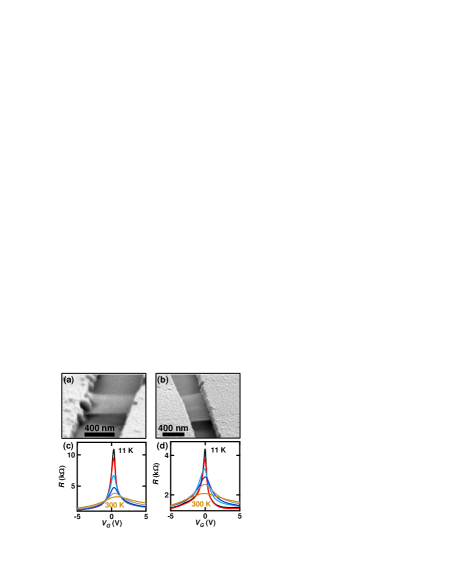
Figure 1 (a)-(b) shows tilted SEM images of Sample A and B respectively (Sample C in Supplemental MaterialSM , SM, Fig. S1). We confirmed using optical contrast and Raman spectroscopy that all three samples are single-layer graphene. Sample A is 650 nm long, 675 nm wide, and suspended 140 10 nm above the substrate (AFM measurement) which consists of 100 2 nm of SiO2 (ellipsometry measurement) on degenerately-doped Si which is used as a back-gate electrode. Sample B is 400 nm long, 1.05 m wide, and suspended 175 10 nm above a 74 2 nm SiO2 film on Si. To prepare the samples, we used exfoliated graphene, and standard e-beam lithography to define Ti(5nm)/Au(80nm) contacts. The samples were suspended with a wet BOE etch such that their only thermal connection is to the gold contacts. We annealed the devices using Joule heating in situ by flowing a large current in the devicesBolotin et al. (2008) (up to 540, 840 and 837 A for A, B and C). Annealing and subsequent measurements were done under high vacuum, Torr.
Panels (c) and (d) show DC two-point resistance data, , for Samples A and B respectively after annealing, versus gate voltage, , which controls charge density. From the width of the maximum at 11 K, we extract a half-width-half-maximum, HWHM, of 0.45, 0.6 and 0.95 V for Samples A, B, C (Sample C, Fig. S1). Using a parallel plate model for the gate capacitance of the devices, these HWHMs correspond to an impurity induced charge densityDu et al. (2008) of 1.5, 1.7 and 2.1 cm-2.

The devices were fabricated with large contact areas between the gold electrodes and graphene crystals, 1.1 to 3 per contact, to minimize the contact resistance, . An upper bound for can be extracted from the two-point curve in Fig. 1(c) by fitting the data (SMSM section 2) with the expressionCastro et al. (2010) where is the resistance due to neutral scatterers plus , is the length of the device, the width, the charge density induced by , the mobility, and the electron’s charge. We fit the data at 100 K for () 1.3 V to avoid the thermal smearing around the Dirac point, . The extracted mobility for Sample A in the doped regime is cm2/V.s at 100 K, and 682 53 and 1135 80 for hole and electron doping respectively. The difference between hole, and electron doping, , is understood as an additional barrier for the electron due to -doping from the gold electrodes Castro et al. (2010). At the Dirac point, we let 908.5 for Sample A. For Sample C, we find 1097 . We note that is much smaller than of Samples A and C, therefore has at most a modest impact on our measurements in these devices. It is not possible to extract for Sample B because it enters the ballistic regime away from the Dirac point (doped regime)Sam . The contact areas of Sample B are larger, and its width wider, than for Samples A and C. Assuming a similar resistance per unit area as for A and C, we expect 657 for B. Based on the reported thermal conductance of Au/Ti/Graphene and Graphene/SiO interfacesKoh et al. (2010), the thermal resistance of our contacts are several orders of magnitude lower than the one we measure below for graphene. Thus, the thermal resistance of the contacts can safely be neglected.
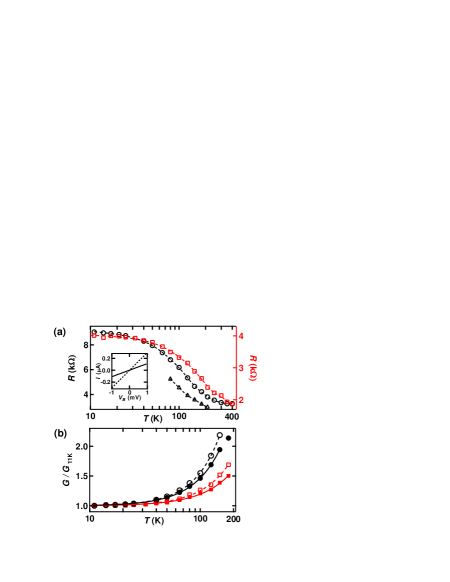
Figure 2(a) shows vs cryostat temperature, , calibration curves for Samples A (circles, left axis), B (squares, right axis), and C (triangles, left axis) near . data are extracted from the slope of the data as shown in the inset of panel (a) at 11 K (solid) and 300 K (dashed), for 1 mV bias where no Joule heating effect is present (). The data are taken at 0.5 V close to 0.33 V for Sample A, and at 0 V for Samples B and C ( -0.1 and 0.07 V), corresponding to 5.7, 2.9, and -1.5 cm-2. The dependence of the data shows an insulating behavior up to 200 K for Sample A and C, and up to 300 K for Sample B. The interpolated dashed lines in panel (a) will be used as thermometry curves to monitor . Note that the thermometry is most accurate where the curves are steepest.
Figure 2(b) shows the relative conductance in the intrinsic regime extracted from panel (a) for Sample A and B. The dependence of in graphene, at low charge density, is strongly dependent on the type of charge transport. For ballistic transport, we expect a very weak temperature dependence at low , and a linear dependence when Muller, Brauninger, and Trauzettel (2009). In the diffusive regime, the expected temperature dependence depends on the type of charge scatterers, and with -1, 0, 2 for acoustic phonon, short-range (neutral), and long-range (charged) scatterers respectively Das Sarma and Hwang (2013); Das Sarma et al. (2011). The temperature dependence of real samples is expected to combine all three types of scattering. We fit the data with a function , and extract = 1.85, 1.74, 1.72 and 1.63 0.03 for Sample A with and 0 (open and filled circles), and Sample B with 657 and 0 (open and filled squares). This -dependence strongly supports diffusive charge transport dominated by long-range charge impurities, as reported in previous experiments on high-mobility devices Bolotin et al. (2008); Das Sarma et al. (2011) and expected theoretically Das Sarma and Hwang (2013). The small departure from a dependence is expected as the samples are not exactly at the Dirac point. We conclude that all samples are in the diffusive regime at low charge density (Fig. 2(b) and SM section 3) and scattering is predominantly due to charged impurities. The data in Fig. 2(a), and its agreement with theory, serves as a reliable thermometer for in our devices.

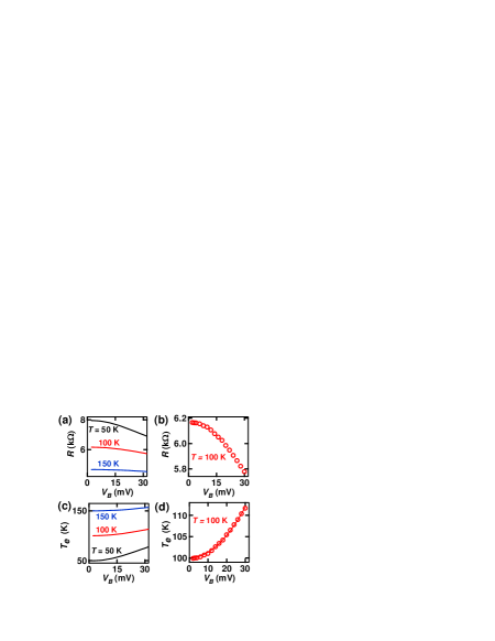
After establishing the thermometry, we demonstrate controlled Joule self-heating of the electrons to apply a thermal bias between the suspended graphene and the electrodes. Figure 3(a) shows vs for Sample A at 50, 100, 150 K (for Samples B and C see Figs. S3 and S4). Panel (b) shows the details of the data at 100 K. decreases monotonically with increasing , at all . We argue that this change in the vs data is caused by Joule heating of the sample. Other mechanisms which could cause a non-linear relation include: scattering from flexural phonons, in-plane optical phonons, substrate phonons, and Zener-Klein tunneling. We restrict our measurements to meV. This rules out any change due to scattering from optical in-plane phonons, 200 meV, and flexural phonons, 70 meV, in grapheneDas Sarma et al. (2011). Phonons in the substrate can also be ruled out as the samples are suspended. The contribution of Zener-Klein tunneling to non-linearity was only observed in very low-mobility devices, and at mV Vandecasteele et al. (2010). This leaves Joule heating as the only plausible cause for the observed vs behavior Viljas et al. (2011). Using the calibration curve for the samples, Fig. 2(a), and data from Fig. 3(a)-(b), we extract the average vs , as shown for Sample A in Fig. 3(c)-(d). In Fig. 3(d), we fit a power law (solid line) , and find 2.00 0.04, as expected for Joule heating over a small range where and do not change appreciably (Samples B and C, SM section 4). Figs. 3(d), S3(d), S4(d) show that the accuracy with which can be extracted is much better than 1 K. We calculate errors from the scatter of the data in panel (d), and similar plots at each , to vary from 0.2 K (steepest regions of Fig. 2(a)) up to 2 K (flat regions of Fig. 2(a)). The smooth dependence of on at all is consistent with electrons having a well defined temperature, as predicted by calculations of the collision lengthLi and Das Sarma (2013) (SM section 5). This is also confirmed by the data shown below.
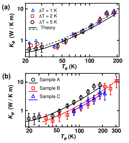
Since our devices are much wider than the elastic mean-free path (SM section 3), the effect of their edges on transport should be small. We use a 1-d heat equation to extract in our devices: where is the Joule heating power per unit volume, the width, the length, and = 0.335 nm the thickness. Using boundary conditions at the two ends (contacts) of the flake, we find . Averaging over the length we find, . Finally, , where . Using and from Fig. 3 and similar plots, for = 1, 2 and 5 K we extract vs in Fig. 4(a) for Sample A. Panel (b) shows vs for all three samples for = 5 K. Data in Fig. 4 show a strong dependence on ranging from roughly 0.5 W/K.m at 20 K to 11 W/K.m at 300 K. The range is limited to the region where we have accurate thermometry (Fig. 2(a)), up to 200 K for A and C, and 300 K for B. Error bars representing the total uncertainty on are shown for the 5 K data (see SM section 6). If the needed to apply were to dope significantly the samples, it could affect the measured . Using (SM section 3)Dorgan, Bae, and Pop (2010), we define an effective chemical potential . For instance, at = 100 K, 18, 18.4 and 19.5 meV respectively for the three devices. The necessary to achieve 5 K in Fig. 4 is always smaller than . We only observe a change in the extracted values when exceeds 8 K, and . Thus does not affect our , with the caveat that we cannot extract precisely at 0. The thermoelectric voltages in our devices are negligible compared to Zuev, Chang, and Kim (2009); Hwang, Rossi, and Das Sarma (2009).

We compare our data with the usual model for diffusing particles in 2-dimensions, . If the heat flow is due to charge carriers, then the specific heat is , the velocity is m/s, and the mean free path is the same as for charge transport. We find (SM section 3), , , and = 71 (85), 47 (59), and 37 (51) nm on average over the range with 0 (). We calculate using the density of states for graphene and the Fermi-Dirac distribution (SM section 7). We plot in Fig. 4(a)-(b) as solid lines with 0. They capture the quantitative dependence of our data. The data points are in good quantitative agreement with the calculated values for all three samples, and especially for Samples A and C. The dashed line in panel (a) shows if we use . If we account for , i.e smaller , changes by the same magnitude as but in the opposite direction (not shown for clarity). The quantitative agreement between data and theory is not as accurate for Sample B since its is smaller than for Samples A and C, and the impact of could be bigger. The data and calculations shown in panel (b) with 0 are within 20, 30, and 15 of each other for Samples A, B and C. If we include , which overestimates the effect due to , the agreement between the data and theory for Sample B is at worst within a factor of two, and much better for Samples A and C. We fit a power law expression over = 45 - 185 K for Samples A and B, and find = 1.73 0.15 and 1.63 0.13 which is very close to the fit on , = 1.62 and 1.59. This agreement is preserved even if we let . As expected goes to 2 when . We conclude that the data is consistent with heat being carried by particles moving with the and of the charge carriers. The magnitude of reaches 11 W / K.m at 300 K with 1.7 - 2.1 cm-2.
A condition to make reliable measurements is that all of the Joule heat remains in the carriers until they diffuse to the leads. Both experiments and theory confirm that the electron-phonon energy transfer in high mobility graphene, at low , is very small below 300 K Gabor et al. (2011); Song et al. (2011); Viljas et al. (2011); Das Sarma and Hwang (2013), and decreases at lower and . In our devices, we extract a cooling length for hot electrons (SM section 8), 100 to 10 m for 20 to 300 K. Since is much longer than , and below the energy of optical phonons, we expect and to be decoupled in our devices when 0, and all of the Joule heat to be carried to the contacts by charge carriers. Indeed, the we measure are two to three orders of magnitude lower than the reported phonon thermal conductivity in graphene Balandin (2011); Pop, Varshney, and Roy (2012).
In summary, we fabricated high quality suspended graphene devices, developed self-thermometry and self-heating methods to extract and control , and the electronic thermal conductivity in graphene. We extracted in the quasi-intrinsic regime, 1.7 - 2.1 cm-2, from 20 K to 300 K. The data in three different devices are in very good agreement with a model where heat is carried by diffusing Dirac quasiparticles. Our results provide evidence that the dominant electron cooling mechanism in intrinsic sub-micron graphene devices below 300 K is hot-electron diffusion to the leads. The theoretical model we use naturally leads to the Wiedemann-Franz relation in the doped-regime and suggests that it should be obeyed in graphene. We thank Andrew McRae for discussions. This work was supported by NSERC, CFI, FQRNT, and Concordia University. We made use of the QNI cleanrooms.
References
- Butler et al. (2013) S. Z. Butler, S. M. Hollen, L. Y. Cao, Y. Cui, J. A. Gupta, H. R. Gutierrez, T. F. Heinz, S. S. Hong, J. X. Huang, A. F. Ismach, E. Johnston-Halperin, M. Kuno, V. V. Plashnitsa, R. D. Robinson, R. S. Ruoff, S. Salahuddin, J. Shan, L. Shi, M. G. Spencer, M. Terrones, W. Windl, and J. E. Goldberger, ACS Nano 7, 2898 (2013).
- Bistritzer and MacDonald (2009) R. Bistritzer and A. H. MacDonald, Phys. Rev. Lett. 102, 206410 (2009).
- Tse and Das Sarma (2009) W. K. Tse and S. Das Sarma, Phys. Rev. B 79, 235406 (2009).
- Kubakaddi (2009) S. S. Kubakaddi, Phys. Rev. B 79, 075417 (2009).
- Berciaud et al. (2010) S. Berciaud, M. Y. Han, K. F. Mak, L. E. Brus, P. Kim, and T. F. Heinz, Phys. Rev. Lett. 104, 227401 (2010).
- Efetov and Kim (2010) D. K. Efetov and P. Kim, Phys. Rev. Lett. 105, 256805 (2010).
- Song, Reizer, and Levitov (2012) J. C. W. Song, M. Y. Reizer, and L. S. Levitov, Phys. Rev. Lett. 109, 106602 (2012).
- Betz et al. (2012) A. C. Betz, F. Vialla, D. Brunel, C. Voisin, M. Picher, A. Cavanna, A. Madouri, G. Feve, J. M. Berroir, B. Placais, and E. Pallecchi, Phys. Rev. Lett. 109, 056805 (2012).
- Betz et al. (2013) A. C. Betz, S. H. Jhang, E. Pallecchi, R. Feirrera, G. Feve, J. M. Berroir, and B. Placais, Nature Phys. 9, 109 (2013).
- Graham et al. (2013) M. W. Graham, S. F. Shi, D. C. Ralph, J. Park, and P. L. McEuen, Nature Phys. 9, 103 (2013).
- Das Sarma et al. (2011) S. Das Sarma, S. Adam, E. H. Hwang, and E. Rossi, Rev. Mod. Phys. 83, 407 (2011).
- Saito, Nakamura, and Natori (2007) K. Saito, J. Nakamura, and A. Natori, Phys. Rev. B 76, 115409 (2007).
- Gabor et al. (2011) N. M. Gabor, J. C. W. Song, Q. Ma, N. L. Nair, T. Taychatanapat, K. Watanabe, T. Taniguchi, L. S. Levitov, and P. Jarillo-Herrero, Science 334, 648 (2011).
- Song et al. (2011) J. C. W. Song, M. S. Rudner, C. M. Marcus, and L. S. Levitov, Nano Lett. 11, 4688 (2011).
- Ghosh et al. (2008) S. Ghosh, I. Calizo, D. Teweldebrhan, E. P. Pokatilov, D. L. Nika, A. A. Balandin, W. Bao, F. Miao, and C. N. Lau, Appl. Phys. Lett. 92, 151911 (2008).
- Freitag et al. (2009) M. Freitag, M. Steiner, Y. Martin, V. Perebeinos, Z. H. Chen, J. C. Tsang, and P. Avouris, Nano Lett. 9, 1883 (2009).
- Seol et al. (2010) J. H. Seol, I. Jo, A. L. Moore, L. Lindsay, Z. H. Aitken, M. T. Pettes, X. S. Li, Z. Yao, R. Huang, D. Broido, N. Mingo, R. S. Ruoff, and L. Shi, Science 328, 213 (2010).
- Jo et al. (2011) I. Jo, I. K. Hsu, Y. J. Lee, M. M. Sadeghi, S. Kim, S. Cronin, E. Tutuc, S. K. Banerjee, Z. Yao, and L. Shi, Nano Lett. 11, 85 (2011).
- Balandin (2011) A. A. Balandin, Nature Materials 10, 569 (2011).
- Pop, Varshney, and Roy (2012) E. Pop, V. Varshney, and A. K. Roy, MRS Bulletin 37, 1273 (2012).
- Dorgan et al. (2013) V. E. Dorgan, A. Behnam, H. J. Conley, K. I. Bolotin, and E. Pop, Nano Lett. , Articles ASAP (2013).
- (22) See Supplemental Material at for images of Sample C, data on and discussion of the contact resistance and mean-free path, self-heating data in Sample B and C, electron-electron scattering length, error analysis, specific heat calculations, and electron cooling length estimate. .
- Bolotin et al. (2008) K. I. Bolotin, K. J. Sikes, Z. Jiang, M. Klima, G. Fudenberg, J. Hone, P. Kim, and H. L. Stormer, Solid State Communications 146, 351 (2008).
- Du et al. (2008) X. Du, I. Skachko, A. Barker, and E. Y. Andrei, Nature Nanotech. 3, 491–495 (2008).
- Castro et al. (2010) E. V. Castro, H. Ochoa, M. I. Katsnelson, R. V. Gorbachev, D. C. Elias, K. S. Novoselov, A. K. Geim, and F. Guinea, Phys. Rev. Lett. 105, 266601 (2010).
- (26) In the doped regime (away from the Dirac point) and at low temperature, the R vs T data for Sample B are consistent with ballistic electron transport. These data will be discussed in a future publication .
- Koh et al. (2010) Y. K. Koh, M. H. Bae, D. G. Cahill, and E. Pop, Nano Lett. 10, 4363 (2010).
- Muller, Brauninger, and Trauzettel (2009) M. Muller, M. Brauninger, and B. Trauzettel, Phys. Rev. Lett. 103, 196801 (2009).
- Das Sarma and Hwang (2013) S. Das Sarma and E. H. Hwang, Phys. Rev. B 87, 035415 (2013).
- Vandecasteele et al. (2010) N. Vandecasteele, A. Barreiro, M. Lazzeri, A. Bachtold, and F. Mauri, Phys. Rev. B 82, 045416 (2010).
- Viljas et al. (2011) J. K. Viljas, A. Fay, M. Wiesner, and P. J. Hakonen, Phys. Rev. B 83, 205421 (2011).
- Li and Das Sarma (2013) Q. Li and S. Das Sarma, Phys. Rev. B 87, 085406 (2013).
- Dorgan, Bae, and Pop (2010) V. E. Dorgan, M. H. Bae, and E. Pop, Appl. Phys. Lett. 97, 082112 (2010).
- Zuev, Chang, and Kim (2009) Y. M. Zuev, W. Chang, and P. Kim, Phys. Rev. Lett. 102 (2009).
- Hwang, Rossi, and Das Sarma (2009) E. H. Hwang, E. Rossi, and S. Das Sarma, Phys. Rev. B 80 (2009).