Cation diffusion and hybridization effects at the Mn-GaSe(0001) interface probed by soft X-ray electron spectroscopies
Abstract
The electronic properties of the Mn:GaSe interface, produced by evaporating Mn at room temperature on a -GaSe(0001) single crystal surface, have been studied by soft X-ray spectroscopies. Substitutional effects of Mn replacing Ga cations and Mn-Se hybridization effects are found both in core level and valence band photoemission spectra. The Mn cation valence state is probed by XAS measurements at the Mn L-edge, which indicate that Mn diffuses into the lattice as a Mn2+ cation with negligible crystal field effects. The Mn spectral weight in the valence band is probed by resonant photoemission spectroscopy at the Mn L-edge, which also allowed an estimation of the charge transfer and Mott-Hubbard energies on the basis of impurity-cluster configuration-interaction model of the photoemission process. The charge transfer energy is found to scale with the energy gap of the system. Competing effects of Mn segregation on the surface have been identified, and the transition from the Mn diffusion through the surface to the segregation of metallic layers on the surface has been tracked by core-level photoemission.
pacs:
Valid PACS appear hereI Introduction
The III-VI semiconductors GaSe, InSe, GaTe, and GaS have received considerable interest in the last few years because they show remarkable nonlinear optical properties and they are regarded as promising materials for photo-electronic applications 010 ; 020 ; 030 ; 001 ; 002 , even in the form of nanowires004 . In the particular case of GaSe and GaS, the interest on these systems has been recently renewed due to the possibility to obtain ultrathin layer transistors based on atomic-thin sheets 003 .
The magnetic properties of these systems doped with transition metal ions (e.g. Mnpekarek , or Fepekarek2001 -doped GaSe) are also under investigation with the aim to find out new classes of diluted magnetic semiconductors (DMS) of the form AMxBVI, where AIIIBVI is a III-VI semiconductor and M is a transition metal ion. For instance, Mn has been incorporated into in samples grown from the melt, and intriguing magnetic properties have been found pekarek . A short range anti-ferromagnetic ordering has been invoked to explain the rather complex magnetic behavior, but a clear identification of the short range coupling mechanisms related to these experimental evidences is still missing. Moreover, a clear understanding of the interplay between magnetism and electronic properties has not yet been reported so far, mainly due to the difficulty of growing high quality Mn-doped single crystals and control both the doping level and possible phase segregations or the creation of defects and vacancies upon doping. Also the local structure around Mn atoms at the Mn:GaSe interface has not yet been probed, being the mechanism of Mn diffusion in the lattice poorly investigated. This can be important in order to relate the observed magnetic behavior to either direct or superexchange interactions through or bonds, respectively.
Furthermore, recent studies lovejoy1 ; lovejoy2 on the Mn:Ga2Se3 system have drawn the attention on this interface, that is strictly related to the one we are currently studying. The magnetic properties of the Mn:Ga2Se3 system have also been reported dubinin2011 , suggesting weak antiferromagnetic correlations in the bulk crystal.
Like the II-VI DMS, substitutional magnetic ions in the III-VI DMS are found in a (distorted) tetrahedral environment. However, in sharp contrast to the II-VI DMS, the III-VI semiconducting host presents a two dimensional (2D) nature, at the origin of the renewed interest in ultrathin layers of, e.g., GaSe and GaS 003 . The weak van der Waals bonding between the stacked four atom thick layers (Se-Ga-Ga-Se) further enhances the two-dimensional nature of this crystal. Because of its markedly nearly 2D structure, GaSe has been considered in the past for angle-resolved photoemission (ARPES) experiments, and a recent study has refocused the interest on this aspect by providing high quality ARPES data supported by band structure calculations of the bulk crystalplucinki , while electronic structure calculations and optical spectroscopy experiments on few-layer GaSe sheets have been recently published ryb .
The present study is focussed on the electronic properties of the Mn-GaSe interface obtained by evaporating Mn ions on the (0001) surface of a ultra-high vacuum cleaved -GaSe single crystal. In the first part, we track the evolution of the Mn-GaSe interface by evaporating at room temperature (RT) increasing quantities of Mn on the GaSe surface. In this way we identify the interface growth regimes, and in particular the balance between cation diffusion through the surface and cation segregation at the surface. Once the interplay between these processes was assessed, we prepared a Mn:GaSe interface where the Ga1-xMnxSe surface alloying through cation diffusion is dominant over Mn segregation on the surface, and we studied the electronic properties through resonant photoemission and X-ray absorption spectroscopies. A comparison is drawn with the Mn:CdTe interface, which displayed a similar transition from cation diffusion to cation segregation processes, as discussed in Ref.attenutaion . This puts on a solid ground the early speculations on the substitution of Ga by Mn in the GaSe lattice, and provides an experimental evidence of the capability of Mn to diffuse into the GaSe lattice. The similarity of the present spectroscopic data with those found for Cd1-xMnxTe indicates that the diffusion process is rather efficient across the surface of the GaSe system. Finally, a characterization of the magnetic properties is reported, based on a study the temperature dependence of the magnetization.
II Experimental details
The GaSe single crystals have been grown by the Bridgman method AGU . The crystals were cleaved in ultra-high vacuum conditions prior Mn evaporation. Mn layers were deposited at RT by in-situ electron beam evaporation from an outgassed Mo crucible loaded with metallic Mn flakes. An Omicron EFM-3 triple evaporator was used in all experiments. The deposition rate was properly calibrated before evaporation on the GaSe cleaved surface. Three interfaces have been produced during the experiments. (i) The first was obtained by evaporating Mn with a constant flux of 500 nA measured across the exit slit of the evaporator. No post-growth annealing was carried out. The data collected from this interface are reported in Section III.A. After an overall 180 second deposition at this rate, the amount of deposited Mn was estimated to be 2 ML. The second sample (Section III.B) was obtained by evaporating 2.4 ML of Mn, and by annealing the interface at 400 ∘C in ultra-high vacuum for 10 minutes to favor the Mn diffusion process in the GaSe lattice. (iii) The third sample (Section III.C-III.E) was produced at the BACH beamline, by depositing a sub-ML of Mn at room temperature. As in the previous case, a 10 minute annealing in ultra-high vacuum at 400 ∘C was carried out after the Mn evaporation.
X-ray absorption and resonant photoemission spectroscopy measurements were performed at the BACH beam line of the Elettra Synchrotron Light Source. The X-ray photoemission (XPS) data have been collected at the Surface Science and Spectroscopy Lab of the Universitá Cattolica (Brescia, Italy) with a non-monochromatized dual-anode PsP x-ray source and a SCIENTA R3000 analyser, operating in the transmission mode, which maximizes the transmittance and works with a 30∘ acceptance angle. The stoichiometry of the Mn:GaSe interfaces produced during the experiments was estimated by measuring the peak area of the Mn, Ga or Se atomic species, properly weighed by the photoemission cross sections and the analyzer transmission. The surface sensitivity (XPS probe depth) at the various kinetic energies (KE) was evaluated by Monte-Carlo calculations of the depth distribution function with the algorithm described in Ref.WernerDDF , in order to include inelastic as well as elastic electronic scattering, in the so-called transport approximationJablonskiTA . We define the calculated probe depth for photoemission as the maximum depth from which 95% of all photo-emitted electrons can reach the surface. In case of exponential attenuation of the signal, this would correspond to three times the electron escape depth.
Magnetic measurements have been performed by means of a SQUID magnetometer. A 5 kOe magnetic field has been applied parallel to the sample plane to study the temperature dependence of the magnetization in the range 2-360 K. A hysteresis cycle has been also collected at room temperature with magnetic field ranging between 10 kOe.
III Results and discussion
III.1 Cation diffusion vs. surface segregation
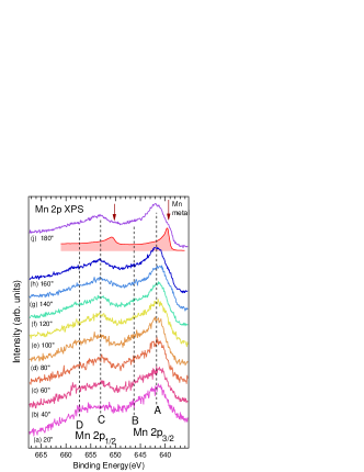
In Figure 1 a sequence of Mn 2p XPS spectra collected after each Mn evaporation at RT on the freshly cleaved -GaSe surface is shown. As can be noticed, the Mn 2p3/2 and Mn 2p1/2 spin-split features of the Mn 2p core line are detectable. Each spin-orbit split component is composed of two broad peaks, denoted as A and B for the 2p3/2 component, and C and D for the 2p1/2 component. These spectra are typical of Mn in DMS, as will be discussed in the next Subsection. Furthermore, the overall Mn 2p lineshape changes as the amount of deposited Mn increases. In particular, starting from spectrum (f) (120 seconds) a peak ascribed to metallic Mn is clearly detectable on the low BE side of the Mn 2p main line, with a BE of 638 eV. The Mn 2p XPS spectrum of a Mn thick film is also shown below spectrum (j) (shaded area), to help identifying the contribution of metallic Mn in the data.
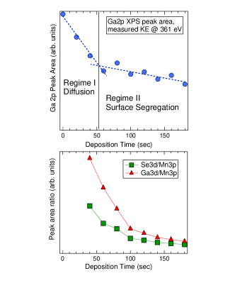
In parallel with the Mn 2p core levels, also the Ga 2p core lines have been collected. The integrated peak area of the Ga 2p is shown in the top panel of Figure 2. The Ga 2p signal attenuation with deposition time is well detectable. The low kinetic energy of the Ga 2p electrons makes the spectra more sensitive to the surface layers. It is important to note that the Ga 2p attenuation seems to follow two regimes. From 0 to about 50 seconds the attenuation is steeper than that measured after 50 seconds. A similar behavior was found for Mn deposited on CdTe single crystals, and ascribed to Cd substitution with Mn attenutaion ; sanga10 . As in that case, we can ascribe the early steep decrease to Ga cation substitution with Mn (corresponding to Cd cation substitution with Mn in the CdTe host crystal), and the following slower decrease with an overall screening of the Ga signal due to the growth of a Mn overlayer on the crystal surface. Therefore, after a determined Mn coverage, Mn diffusion to layers underneath the surface and Ga substitution processes are hindered, resulting in the build-up of Mn overlayers on the surface.
It should be noted that electrons from the Ga 2p core levels are emitted with a kinetic energy of 361 eV. The XPS probe in GaSe for these electrons is quite surface sensitive, as the calculated probe depth is about 2.5 nm. Unfortunately, Se does not display core levels with a comparable kinetic energy, as was the case of Cd 3d and Te 3d attenutaion , and it is not possible to evaluate differences in the signal attenuation rate of Se surface sensitive emission with respect to the Ga 2p case. To overcome this limit, a set of shallow core levels (Se 3d, Mn 2p, and Ga 3d) with much higher kinetic energies (about 1450 eV) has been collected. With this KE, the probe depth is about 7.5 nm for the three shallow core level emissions. On this basis, the Ga3d/Mn3p and Se3d/Mn3p ratio vs. deposition time are shown in the bottom panel of Fig.2. As can be observed, Ga and Se signal have a steep decrease down to about 100 sec Mn deposition time, and Ga decreases more rapidly than Se, suggesting that Ga is substituted by Mn in the lattice. Above this limit both Ga 3d and Se 3d shallow core levels display a much lower signal attenuation, indicating that different mechanisms are at work to screen the photoemission signal, very likely the prevalent growth of a Mn overlayer on the surface. Consistently with the higher probe depth, the change of growth regime here is found around 100 seconds rather than at about 60 seconds. We rationalize this finding by assuming that the substitution of Ga with Mn is achieved at the early stages of deposition for the topmost Ga layers (preferentially probed by the Ga 2p attenuation), while the substitution mechanism in the underlying layers remains active also at further deposition steps, determined by the kinetics of Mn diffusion processes.
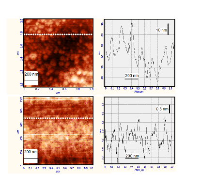
The build up of Mn on the surface leads to distinct features of the sample surface, as shown in Fig.3, top panel. In fact, while the freshly cleaved surface shows a quite flat profile with reduced roughness (Fig.3, bottom panel), the surface obtained after the last deposition stage is quite rough, with round-shaped protrusions that could be related to Mn segregation on the surface.
The Mn stoichiometry in the Ga1-xMnxSe alloy was also estimated by measuring the intensity of the Mn 2p core level peak with respect to the Ga 3d and Se 3d core lines. After proper normalization to photoemission cross-sections and analyzer transmission, assuming a uniform distribution of Mn ions through the topmost surface layers, the amount of Mn diffused into the crystal after 60” evaporation (spectrum (c) of Fig.1, roughly at the border between the two deposition regimes evidenced in the bottom panel of Fig.1) resulted to be x=0.0560.005 in Ga1-xMnxSe.
III.2 Core level photoemission of the Ga1-xMnxSe alloy
After the preliminary work so far described, we have been able to identify the spectroscopic signatures of the conditions where the alloying process, yielding Ga1-xMnxSe, was dominant over the Mn segregation on the surface. The Mn evaporation was repeated on freshly cleaved GaSe surfaces and, after Mn evaporation, annealing at 400 ∘C in ultra high vacuum was also carried out to further induce the alloying process through diffusion. The amount of evaporated Mn (2.4 ML) exceeds the overall amount of Mn of Section III.A by a factor 1.2, and a larger contribution of metallic Mn is expected before annealing. However, the larger amount of Mn allowed us to collect data with a a better statistics and obtain a good reference Mn 2p XPS spectrum of the Mn:GaSe alloy after the annealing treatment.
Figure 4 shows the Mn 2p core line of the Mn:GaSe interface prior and after annealing in vacuum. As observed, the four spectral features of the vacuum annealed interface present strong satellites (B and D) on the high BE side of the main lines (A and C) of the Mn 2p spin-orbit split components.
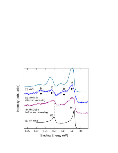
We can exclude the presence of relevant oxygen contaminations, as the measured Mn 2p XPS lineshape is quite different from that of MnO (Figure 4-d). Furthermore, we did not observe any signal from oxygen within the sensitivity of our probe. The spectrum of the as-deposited film (Figure 4-b) shows two broad spin-orbit split components, suggesting the presence of several contributions that could be ascribed to both metallic Mn and Mn diluted in the GaSe lattice. In fact, a comparison with the Mn 2p XPS core line from metallic Mn (Figure 4-a) indicates that the M1 and M2 features (marked by dashed vertical lines) can be ascribed to metallic Mn. These features are progressively quenched with annealing treatments (Figure 4-c), indicating that the annealing is quite effective to prevalently induce a substitution of Ga by Mn atom, rather than a clustering of Mn on the GaSe(0001) surface.
The peaks A and C are separated by the spin-orbit interaction and the width of these two peak is ascribed to disorder effects, related to replacement of Ga atom by Mn. On the high BE side of these peaks, two satellites are also detectable (B and D), quite similar to those found in Mn-based DMS, such as Cd1-xMnxTe, Zn1-xMnxS and Ga1-xMnxAs sanga10 ; sanga11 ; okabaya . They are ascribed to charge transfer effects from the ligand anions (Te, S or As, respectively) to the 3d levels of Mn cations. These effects are usually accounted for in the frame of a configuration interaction model where the electronic states involved in the photoemission process are described by a linear combination of several configurations (see, e.g. Ref okabaya and Refs. therein) such as 3dn, 3dn+1L, 3d,where L represents a hole in the ligand created by the charge transfer. The ligand-to-3d charge-transfer energy is defined by =E(dn+1)-E(dn). The intensity of B and D satellites varies depending on the charge transfer energy , as well as on the hybridization strength (T) between the p and d orbitals involved in the charge transfer process (here from Se to Mn ). Therefore, the line-shape analysis of the Mn 2p core levels shown in Figure 4 provides an evidence of Mn-Se hybridization effects for the Mn:GaSe system. In Subsection D, a detailed calculation of the Mn spectral weight in photoemission through CI models will be carried out for the 3d levels in the valence band region.
Finally, it is rather important to compare the present results with those obtained on the Fe-GaSe interfaceiron1 ; iron2 . The analysis of Fe 2p XPS lineshape in the Fe-GaSe interface does not provide evidence of Fe-Se hybridization, being the Fe 2p XPS spectra quite similar to that of metallic Fe, while Fe clustering effects are found to be dominant. In turn, our measurements on the electronic properties of the Mn:GaSe interface have shown the capability of Mn to diffuse into the lattice with a remarkable hybridizations with Se anions.
At this stage we cannot exclude that annealing in vacuum can also trigger Mn desorption effects, but the results of the first deposition (Section III.A) clearly indicate that alloying (i.e. Mn diffusion though the lattice and Ga substitution with Mn without resorting to any annealing) is the dominant process. According to the GaSe layered crystal structure, the UHV cleaving should occur between the two facing Se layers (i.e. through a breaking of the Se-Se weak van der Waals bonds). The weakness of this bond should also favor the diffusion of Mn through the lattice between the Se layers, and eventually the Mn hybridization with Se.
III.3 X-ray absorption from the Ga1-xMnxSe alloy
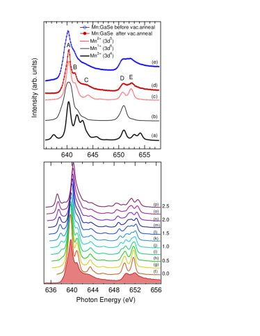
The Mn L-edge XAS spectra are shown in Figure 5. In particular, the data obtained after the Mn deposition (e) and after annealing at 400oC and collected at RT (d) are presented. The as-deposited Mn-doped GaSe (e) shows before annealing the presence of both metallic and a reacted Mn-GaSe interface, as appearing from an overall smooth XAS lineshape, with minor modulations that will ultimately evolve into the post-annealing XAS lineshape (d). Indeed, after annealing at 400oC, sharper features (labeled as A, B, C, D, and E) appear, and the comparison with multiplet calculations for a Mn2+ 2p63d5 2p53d6 electric-dipole allowed transition (c) unambiguously shows that the measured spectrum can be ascribed to a Mn2+ ion in the GaSe matrix. Similar transition calculated for Mn1+ (b) and Mn3+ (a) ions do not fit the experimental data.
The remarkable similarity with the XAS spectrum predicted for the Mn2+ calculation is particularly helpful for the interpretation of the electron spectroscopy results. This will justify the assumption at the basis of CI calculations for the Mn 3d spectral weight in the valence band (see next Section) where an Mn2+ ion will be assumed as the ionic configuration in the parameterized CI model.
In the bottom panel of Figure 5, we have shown a set of calculated Mn XAS spectra in a tetrahedral Td symmetry, starting from zero crystal field to 10Dq=2.5 eV, where 10Dq is the crystal field splitting of the 3d orbitals. It is important to note that crystal field effects seem to be rather limited up to 10Dq=0.75 eV. At this energy, two features appear on the low photon energy sides of the calculated Mn LIII and Mn LII edges, that have no counterpart in the experimental data. Therefore, we assume that crystal field effects are negligible. This remark will also be at the basis of the CI model for the valence band calculations, where crystal field splitting will be set to zero.
III.4 Valence band resonant photoemission at the Mn L-edge
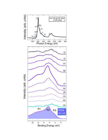
The valence band spectra of the clean GaSe and of the Mn-doped, annealed, GaSe single crystals are shown in Figure 6 (b) and (a), respectively. The photoemission spectra have been collected with a photon energy of 797 eV and have been normalized to the maximum of the valence band emission (peak A). Both spectra show a main line with three features labeled A’, A, and B, and a peak C at higher binding energies. When Mn is evaporated on the GaSe cleaved surface, the main changes that can be observed are the appearance of a feature A” at the Fermi edge, and an increase of the spectral weight in the regions between the peaks A and B and the peaks B and C. The curve displayed in Fig 6 (c) represents the difference between the spectra (a) and (b). This difference confirms the increase of spectral weight upon Mn deposition in the 3-7 eV binding energy range, and in the region just below the Fermi edge (BE=0-2 eV), while a decrease of the intensity is found below peak C after Mn deposition and annealing at 400 ∘C.
The main features of the present experimental data can be interpreted on the basis of the calculated DOS so far published plucinki ; DOS2 ; DOS3 . Indeed, the observed experimental peaks have a counterpart in, e.g., the DOS calculated by Plucinki et al. plucinki that identify three regions (I, II, and III) in the valence band (see Fig.3 of Ref.plucinki ). Region I corresponds to the observed peaks A and A’, region II to peak B and region III to peak C. From the analysis of the projected DOS on Se s,p states and Ga s,p states, it is rather interesting to observe that Ga mainly contributes in the region below peak C, i.e. in the region where a spectral weight decrease is observed upon Mn doping and annealing. This is in agreement with the assumption of Ga substitution with Mn atoms, as remarked in Subsection A. Finally, the states appearing at the Fermi edge (A”) can be ascribed to unreacted Mn at the surface.

In order to enhance the Mn contribution to valence band states, a ResPES study at the Mn 2p-3d absorption edge has been carried out. The results are shown in Fig 7. As first, on the XAS spectrum (top panel) the photon energies (a to j) selected to collect ResPES data are indicated. The whole set of ResPES data is shown in the bottom panel. The data span a photon range across the Mn LIII threshold. The VB spectra show a clear enhancement of the spectral weight with a photon energy of about 640 eV. At this energy a peak around BE= 4.5 eV in the valence band shows a remarkable intensity enhancement. The difference between the resonant (e) and off-resonance (a) spectra (hereafter denoted as resonating spectral weight, RSW) is shown in panel C. Here it is clearly seen that the RSW is determined by a peak at 4.5 eV (R2) and by two broad features at about BE= 6-8 eV (R1) and BE= 1-3 eV (R3).
We have used spectrum (e) rather than (f), as it is known mnge2012 that for spectra collected with photon energies at the maximum of the absorption threshold [spectrum (f) in the present case] the weight of the Auger emission channel is not negligible and the maximum of the valence band emission is already shifted to higher BE with respect to spectrum (e), where the resonant Raman Auger channel (RRAS) is still dominant.
It is worth observing that the large R2 resonance is found in the energy range where the difference spectrum of Fig.6-c shows the largest difference between the doped and undoped surfaces, confirming that a large Mn contribution should be expected at least in this energy range.
Further insight into the origin of the three spectral features (R1, R2, and R3) in the RSW can be obtained at the light of parameterized CI calculations for the valence band.
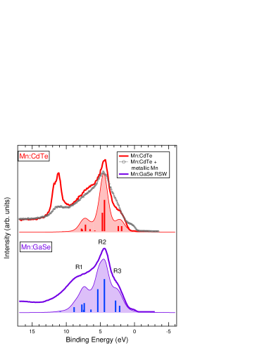
Impurity-cluster CI calculations of the Mn 3d spectral weight are shown in Fig.8. In the CI approach several configurations, denoted as , ( denotes a ligand hole, here a hole on Te 4p orbitals) are used to describe the open shell of the 3d transition metal ion during the photoemission process. The spectral weight in a photoemission experiment is calculated, in the sudden approximation, by projecting the final state configurations () on the the ground state, i.e. where represents the ground state (GS) wavefunction, and the sum is run over all final state configurations with energy . Where required, proper fractional parentage coefficients can be used, as was done in the present case.
The calculations have been carried out following the scheme presented by Fujimori et al. mnconfi for several Mn doped semiconductors, based on a 3d5 initial state of the transition metal atom fuji . The results are shown in Fig.8, along with those obtained on a Mn-doped CdTe single crystal attenutaion . The parameter set used in the calculation is reported in Table 1.
The comparison with the RSW detected under the same conditions for the Mn-doped CdTe crystal is rather interesting. The gray spectrum (empty circles) in the top panel represents the resonance spectrum collected from an heavily doped CdTe single crystal (adapted form Ref. attenutaion ), which shows a contribution at the Fermi level of metallic Mn states similar to the states observed in the GaSe host crystal, though these states are less intense in the GaSe host system. Also in the CdTe case, three peaks appear in the resonant spectrum, but the relative weight and width of these peaks are different from the Mn:GaSe case. Peak R2 is larger in the GaSe host, and the separation between peak R1 and R2 is larger in the GaSe host with respect to the CdTe case. These differences have been considered as constraints in the calculations. In particular, the calculations for the GaSe case have been obtained by setting the crystal field to zero and by considering a larger charge transfer energy (2.95 eV) as compared to the CdTe host (2.0 eV, Table 1). The first assumption is justified by the lack of relevant crystal field effects observed in XAS, whereas the second is justified by the larger band gap of GaSe with respect to CdTe, as the charge transfer energy is usually assumed to scale with the energy gap of the host crystal (Eg=1.49 eV in CdTe, Eg=2.02 eV in GaSe). This choice of the parameter set resulted in a broadening of the calculated peak below R2 and in the intensity increase and BE shift of the calculated spectral weight below R1. Also the calculated spectral weight below R3 is increased, in agreement with the measured data. We used the free ion Racah parameter for Mn2+, B=0.126, C=0.421, and the crystal field was set at 0.4 eV for the CdTe host and 0 eV for the GaSe host.
| Host | U | pd | ||
|---|---|---|---|---|
| Matrix | (eV) | (eV) | (eV) | |
| GaSe | 2.95 | 6.4 | -1.25 | |
| CdTe | 2 | 5 | -1.1 |
III.5 Magnetic properties
Figure 9 shows the temperature dependence of the magnetic susceptibility , evaluated with respect to the unit-mass of the considered sample. The overall susceptibility is always negative disclosing a dominant diamagnetic behavior. This is confirmed by the negative slope of the M vs. H curve measured at room temperature, reported in the inset on Fig. 9. The negative dominant background is not surprising as the GaSe host is diamagnetic and the Mn:GaSe interface represents a small fraction of the sample (few nanometers with respect to the overall single crystal thickness, that is about 100 microns). However, though negative, the magnetic susceptibility curve reveals a signature of paramagnetism, with a decrease of values with temperature that is fit by the curve representing the Curie-Weiss law (continuous line in Fig. 9), with very small Weiss constant value (about -3 K).

This effect can be ascribed to the topmost layers of the sample, i.e. those hosting the Mn dopant after the temperature induced diffusion. This behavior is quite different from that observed in bulk Mn:GaSe single crystals pekarek , which show a complex behavior with a quenching of magnetization at low temperatures, i.e., where we observe the steady increase of paramagnetic signal. The magnetic behavior is also different in many details from that observed for other known bulk phases that can be regarded as possible segregated phases in the growth of the Mn:GeSe interface, such as MnSe and MnSe2 88 ; 99 , and MnGa2Se4 89 . In turn, closer similarities, i.e. a virtually paramagnetic behavior, are found with respect to the case of monoclinic crystals of (Ga1-xMnx)2Se3 discussed in Ref. dubinin2011 .
IV Conclusions
We have been able to prepare well characterized Mn:GaSe interfaces, with evidence of the formation of a Ga1-xMnxSe alloy below the GaSe surface. Alloying is obtained already after evaporation at room temperature. The Mn deposition in the present study spanned two regimes. In the early regime the Mn diffusion through the surface was the dominant mechanism, while in the second regime the segregation of Mn layers on the GaSe surface was the most likely process. Unlike Fe-GaSe interfaces, where iron clustering effects are dominant and no trace of Fe-Se hybridization is found upon the analysis of Fe 2p XPS lineshape iron1 ; iron2 , our measurements on the electronic properties of the Mn:GaSe interface have shown the capability of Mn to diffuse into the lattice with a remarkable hybridizations with Se anions. Magnetic measurements evidence a paramagnetic behavior for the Mn-doped interface, while the dominant behavior is diamagnetic, due to the bulk of the GaSe host crystal.
References
- (1) K. Kato, N. Umemura, Optics Letters, 36, 746 (2011);
- (2) A. Segura, J. Bouvier, M.V. Andres, et al. Phys. Rev. B, 56, 4075 (1997);
- (3) S. Nusse, P.H. Bolivar, H. Kurz, et al., Phys. Rev. B, 56, 4578 (1997);
- (4) H. Ertap, G.M. Mamedov, M. Karabulut, A. Bacioglu, Journ. of Luminescence, 131, 1376 (2011)
- (5) P.A. Hu, Z.Z. Wen, L.F. Wang, P.H. Tan, K. Xiao, ACS Nano, 6, 5988 (2012)
- (6) H. Peng, S. Meister, C.K. Chan, X.F. Zhang, Y. Cui, Nano Letters, 7, 199 (2007)
- (7) D.J. Late, B. Liu, J.J. Luo, A.M. Yan, H.S.S.R. Matte, M. Grayson, C.N.R. Rao, V.P. Dravid, Advanced Materials, 24 3549 (2012)
- (8) T. M. Pekarek, B. C. Crooker, I. Miotkowski and A. K. Ramdas, Journ. of Appl. Phys. 83 6557 (1998)
- (9) T. M. Pekarek, C.L. Fuller, J. Garner , B.C. Crooker, I. Miotkowski, A.K. Ramdas, Journ. of Appl. Phys. 89, 7030 (2001)
- (10) T.C. Lovejoy, E.N. Yitamben, S.M. Heald, F.S. Ohuchi and M.A. Olmstead, Appl. Phys. Lett. 95, 241907, (2009).
- (11) T.C. Lovejoy, E.N. Yitamben, S.M. Heald, F.S. Ohuchi and M.A. Olmstead, Phys. Rev. B 83, 155312 (2011).
- (12) S.F. Dubinin, V.I. Maksimov, and V.D. Parkhomenko, Crystallography Reports, 56, 1165 (2011)
- (13) L. Plucinski, R.L. Johnson, B.J. Kowalski, K. Kopalko, B.A. Orlowski, Z.D. Kovalyuk, G.V. Lashkarev, Phys. Rev. B 68 125304 (2003)
- (14) D.V. Rybkovskiy, N.R. Arutyunyan, A.S. Orekhov, I.A. Gromchenko, I. V. Vorobiev, A.V. Osadchy, E.Y. Salaev, T.K. Baykara, K.R. Allakhverdiev, E.D. Obraztsova, Phys. Rev. B, 84, 085314 (2011)
- (15) L. Sangaletti, S. Pagliara, I. Dimitri, F. Parmigiani, A. Goldoni, L. Floreano, A. Morgante, V.F. Aguekian, Surface Science 566-568 508 (2004)
- (16) M. Yamamoto, H. Mino, I. Akai, T. Karasawa, V.F. Aguekian, Journ. of Luminescence, 87-9, 275 (2000)
- (17) W. S. M. Werner, Surf. Int. Anal. 31, 141 (2001).
- (18) A. Jablonski, Phys. Rev. B 58, 16470 (1998).
- (19) L. Sangaletti, A. Verdini, S. Pagliara, G. Drera, L. Floreano, A. Goldoni, A. Morgante, Phys. Rev. B 81, 245320 (2010)
- (20) L. Sangaletti, M.C. Mozzati, G. Drera, V. Aguekian, L. Floreano, A. Morgante, A. Goldoni, G. Karczewski Appl. Phys. Lett. 96, 142105 (2010)
- (21) J. Okabayashi, A. Kimura, O. Rader, T. Mizokawa, A. Fujimori, T. Hayashi, M. Tanaka, Phys. Rev. B 58 R4211 (1998)
- (22) A.R. de Moraes, D.H. Mosca, W.H. Schreiner, J.L. Guimaraes, A.J.A. de Oliveira, P.E.N. de Souza, V.H. Etgens, M. Eddrief, Journal of Magnetism and Magnetic Materials 272-276, 1551 (2004)
- (23) A.R. de Moraes, D.H. Mosca, N. Mattoso, J.L. Guimaraes, J.J. Klein, W.H. Schreiner, P.E.N. de Souza, A.J.A. de Oliveira, M.A.Z. de Vasconcellos, D. Demaille, M. Eddrief, V.H. Etgens, J. Phys.: Condens. Matter 18, 1165 (2006)
- (24) Zs. Rak, S.D. Mahanti, Krishna C. Mandal, N.C. Fernelius, Journ. of Phys. Chem. of Solids, 70, 344 (2009)
- (25) M.O.D. Camara, A. Mauger, I. Devos, Phys. Rev. B 65, 125206 (2002)
- (26) See, e.g., L. Sangaletti, S. Dash, A. Verdini, L. Floreano, A. Goldoni, G. Drera, S. Pagliara, and A. Morgante, J. Phys.: Condens. Matter 24, 235502 (2012), and Refs. therein
- (27) T. Mizokawa and A. Fujimori, Phys. Rev. B 48 14150 (1993)
- (28) A. Fujimori, M. Sacki, N. Kimizuka, M. Taniguchi, S. Suga, Phys. Rev. B 34 7318 (1986)
- (29) Q. Peng, Y. Dong, Z. Deng, H. Kou, S. Gao, Y. Li, Journ. Phys. Chem. B 106 9261 (2002)
- (30) M. Morocoima, M. Quintero, E. Quintero, J. Gonz lez, R. Tovar, P. Bocaranda, J. Ruiz, N. March n, D. Caldera and E. Calderon, Journ. of Appl. Phys. 100, 053907 (2006)
- (31) J.B.C Efrem D sa, P.A. Bhobe, K.R. Prilkar, A. Das, P.S.R. Krishna, P.R. Sarode, R.B. Prabhu, Pramana-Journal of Physics, 63, 227 (2004)