Stray-field imaging of magnetic vortices with a single diamond spin
Abstract
Despite decades of advances in magnetic imaging, obtaining direct, quantitative information with nanometer scale spatial resolution remains an outstanding challenge. Recently, a new technique has emerged that employs a single nitrogen-vacancy (NV) defect in diamond as an atomic-size magnetometer. Although NV magnetometry promises significant advances in magnetic imaging, the effectiveness of the technique, when applied to realistic magnetic nanostructures, remains to be demonstrated. Here we use a scanning NV magnetometer to image a magnetic vortex, which is one of the most iconic object of nanomagnetism, owing to the small size ( nm) of the vortex core. We report three-dimensional, vectorial, and quantitative measurements of the stray magnetic field emitted by a vortex in a ferromagnetic square dot, including the detection of the vortex core. We find excellent agreement with micromagnetic simulations, both for regular vortex structures and for higher-order magnetization states. These experiments establish scanning NV magnetometry as a practical and unique tool for fundamental studies in nanomagnetism.
Introduction. Although a remarkable number of magnetic microscopy techniques have been developed over the last decades, imaging magnetism at the nanoscale remains a challenging task since it requires a combination of high spatial resolution and sensitivity Freeman_Science2001 . A first approach consists in directly mapping the sample magnetization, which implies sending and collecting back test particles whose interaction with matter has a magnetization-dependent term. This approach provides the highest spatial resolution to date, down to the atomic-scale for spin-polarized scanning tunneling microscopy Wachowiak2002 and about nm in transmission X-ray microscopy Fischer2012 . However, these techniques require highly complex experimental apparatus and a dedicated sample preparation so that the particles can reach and escape from the tested region without perturbations. To observe magnetic samples in their real, unprepared state, a more suited approach consists in mapping the magnetic stray field generated outside the sample, even if this method cannot uniquely determine the actual sample magnetization IEEE . Furthermore, the spatial resolution is then limited both by the probe size and its distance to the sample. Among many stray field microscopy techniques Kirtley2010 , magnetic force microscopy (MFM) has become ubiquitous, as it provides a spatial resolution below 50 nm Martin1987 and operates under ambient conditions without any specific sample preparation. It was for instance the first method that allowed the observation of the core of a magnetic vortex in a thin ferromagnetic disk Shinjo2000 . However, due to the intrinsic magnetic nature of the probe, MFM is known to be perturbative and not easily quantitative Garcia2001 , therefore limiting its field of applications.
Recently, a magnetometer based on the magnetic response of a single nitrogen-vacancy (NV) defect in diamond has been proposed Taylor2008 ; Degen2008 ; Balasubramanian2008 ; Maze2008 , which promises significant advances in magnetic imaging. Indeed, it provides non-perturbing and quantitative measurements of the stray magnetic field, with an unprecedented access to low fields combined with an atomic-sized detection volume Rondin2012 ; Maletinsky2012 . In this letter, we use NV-based magnetometry to measure the stray field emanating from magnetic vortices in nanostructured ferromagnetic thin films. Such structures, which are of great interest both for fundamental studies in nanomagnetism Antos2008 and for applications such as non-volatile magnetic storage Drews2009 ; Pigeau2010 and microwave generation Pribiag2007 , have been investigated using a wide range of microscopy techniques Shinjo2000 ; Raabe2000 ; Chung2010 ; Wachowiak2002 ; Choe2004 ; Vansteenkiste2009 . However, obtaining quantitative information that is directly comparable to theory remains a challenging task. Further, imaging the vortex core, which can be as small as nm and plays a crucial role in the vortex dynamics, is a long-standing goal that has been reached by very few methods only Shinjo2000 ; Wachowiak2002 ; Fischer2012 . Here we show that scanning NV magnetometry enables to quantitatively map the stray field above a thin ferromagnetic square in a vortex state, revealing in 3D the full structure of the magnetic field distribution, including the detection of the vortex core. Furthermore, we demonstrate that the vectorial and quantitative nature of the measurement provide direct comparisons with micromagnetic simulations. This work thus opens new avenues for fundamental studies in nanomagnetism and spintronics.
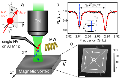
Principle of scanning NV magnetometry. The scanning NV magnetometer combines an optical confocal microscope and an atomic force microscope (AFM), all operating under ambient conditions (see Methods). As sketched in Figure 1(a), a diamond nanocrystal hosting a single NV defect is grafted at the apex of the AFM tip and used as an atomic-sized magnetic sensor Rondin2012 . The NV defect ground state is a spin triplet with a zero-field splitting GHz between a singlet state and a doublet , where denotes the spin projection along the intrinsic quantization axis of the NV defect (Fig. 1(a)). Under optical illumination, the NV defect is efficiently polarized into the spin sublevel and exhibits a spin-dependent photoluminescence (PL) Manson_PRB2006 . These combined properties enable the detection of electron spin resonance (ESR) by optical means Gruber_Science1997 . A typical ESR spectrum of the NV sensor placed in a static magnetic field is shown in Figure 1(b). In the limit of weak magnetic fields ( mT), the spin quantization axis remains fixed by the NV defect axis, and the two ESR frequencies are given by , where is the magnetic field projection along the NV axis and is the electron gyromagnetic ratio (Fig. 1(b)). Note that strain-induced splitting of the spin sublevels has been omitted for clarity purpose (see Supplementary Information). Measurement of the magnetic field through Zeeman shifts of the ESR frequency is therefore quantitative and non perturbing, since the dipolar field from a single NV defect is as low as T at nm distance Taylor2008 .
Stray field imaging of magnetic vortices in ferromagnetic films. In the following, we use the scanning NV magnetometer to map the magnetic stray field generated by magnetic vortices in ferromagnetic thin films. More precisely, we investigate squares of Fe20Ni80 with a thickness of nm and a m side length. This magnetic structure is characterized by a curling in-plane magnetization with a vortex core in the center where the magnetization points out of the plane (Fig. 1(c)). Such a magnetic vortex is an ideal object for evaluating the sensitivity and spatial resolution of any advanced magnetic microscopy technique since the size of the vortex core can reach nm [Fischer2012, ]. Furthermore this magnetic structure is topologically stable and therefore appears as an interesting candidate for memory cells in non-volatile data-storage devices Drews2009 ; Pigeau2010 .
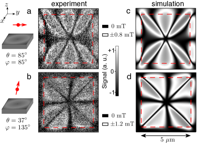
The NV probe is first approached at a distance 300 nm above the magnetic vortex structure. Magnetic field mapping is performed by scanning the sample while measuring the difference of NV defect PL intensity for two fixed microwave (MW) frequencies and , applied consecutively at each point of the scan Rondin2012 . This signal is positive if , i.e. when the local field experienced by the NV defect is , and negative if , i.e. for (see Supplementary Information). The resulting image thus exhibits positive and negative signal regions corresponding to iso-magnetic field contours (,), as well as zero-signal regions for any other field projections. An example of such a dual-iso-B image recorded above a ferromagnetic square is presented in Figure 2(a), revealing a flower-shaped magnetic field distribution. Independent measurement of the NV defect orientation with a calibrated magnetic field indicates that the NV defect is oriented mainly along the axis in this experiment (see Supplementary Information). Hence the magnetic map shown in Figure 2(a) corresponds to the field component that is parallel to the sample surface and along a side of the ferromagnetic square. By properly selecting the orientation of the single NV defect grafted at the apex of the AFM tip, any field component can be similarly measured. For instance, Figure 2(b) is essentially a map of the -component, i.e. the out-of-plane magnetic field. These experiments establish NV-based magnetometry as a unique instrument providing quantitative and vectorial magnetic field images at the nanoscale.
The measured stray field arises from Néel domain walls at the square diagonals which induce volume charges with opposite sign on each side of the wall. The general lobe structure of the magnetic distribution can therefore be qualitatively understood by considering the magnetic field created by an assembly of magnetic dipoles placed along the diagonals. To get more precise predictions, the sample magnetization distribution was first calculated through micromagnetic simulations using OOMMF software oommf , with a cell size of nm3. Once the equilibrium magnetization state found, the magnetic field generated by the structure is computed by summing the contribution of all magnetization cells. This magnetic field is then projected along the experimentally measured NV axis, and the NV defect ESR response is finally applied to get the simulated dual-iso-B image (see Supplementary Information). As shown in Figure 2(c)&(d), the simulations reproduce well the experimental data, including apparent asymmetries which stem from the imperfect alignment of the corresponding NV defects with respect to the and axis. By varying the probe-to-sample distance , it is even possible, as shown in the Supplementary Information, to obtain an overview of the stray field in the half-space above the sample, thus providing a 3D mapping of the magnetic field distribution.
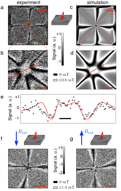
Imaging the vortex core. The magnetic images shown in Fig. 2(a)&(b) are recorded with a probe-to-sample distance of several hundreds of nanometers. At such distances, the stray field linked to the out-of-plane vortex core magnetization cannot be detected. The vortex center therefore appears dark (zero field) both in the images and in the simulations. With the aim of observing the vortex core, the NV probe is brought as close as possible to the sample with the AFM operating in tapping mode. Figure 3(a) shows the dual-iso-B image of the whole square obtained with the NV defect probe used in Fig. 2(b), i.e. mainly oriented along the axis. By zooming in the center of the structure, the vortex core is revealed with an apparent size nm (Fig. 3(b)). Although the spatial resolution of scanning NV magnetometry is ultimately given by the atomic-sized detection volume, the effective resolving power is rather limited by the probe-to-sample distance, a common feature of any stray field microscopy technique. Indeed, numerical calculations indicate that the size of the out-of-plane vortex core magnetization is around nm at the sample surface. The probe-to-sample distance can be estimated by comparing the experimental results to magnetic images simulated at different distances from the sample surface. As shown in Figures 3(c),(d)&(e), a good agreement is obtained for a distance nm. We attribute this relatively large value to an imperfect positioning of the diamond nanocrystal at the apex of the AFM tip. A more precise control of the NV magnetic sensor position could be achieved by using diamond nanopillar-probes Maletinsky2012 . Although the simulation fairly agrees with experimental data, we note that the sharp structures lying along the square diagonals (Fig. 3(c)) are not observed in the experimental images (Fig. 3(a)). In those regions, the stray field generated by Néel domain walls is strong enough to induce a mixing of the NV defect electron spin sublevels which results in an overall reduction of ESR contrast Tetienne2012 (see Supplementary Information).
Chirality and polarity of the vortex state. The vortex structure is commonly characterized by two independent binary properties. The chirality determines whether the in-plane magnetization is curling clockwise () or counterclockwise (), while the polarity of the vortex indicates the upward () or downward () magnetization of the core. The apparent pairing of the zero-field contours around the vortex core observed in Figure 3(b) directly enables us to determine that (see Supplementary Information). We note that only an absolute value of the field is measured, preventing a direct measurement of the core polarity without additional measurements. This limitation could be overcome by addressing selectively one of the two ESR transitions through circularly polarized MW excitation Alegre2007 . Here, we gain further insights into the vortex structure by applying an external bias magnetic field along the -axis with a projection along the NV axis. The amplitude of this external magnetic field is chosen weak enough to avoid modifying the sample magnetization, so that just adds up to the regular stray field of the vortex structure. Figures 3(f)&(g) show magnetic images obtained with mT and mT, respectively. The stray field of the vortex core turns dark – the net magnetic field vanishes – with the negative bias field, which reveals that the vortex core magnetization points upward , and indicates a stray field emanating from the core mT. Conversely, the core field is increased with a positive bias field since it adds up to . From this polarity measurement, the chirality can finally be deduced leading to a full characterization of the vortex structure.
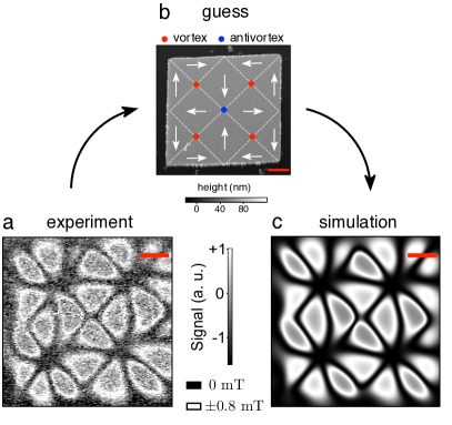
Imaging higher-order magnetization distribution. As a final experiment, we study a higher-order magnetization distribution on a Fe20Ni80 square dot. As shown in Figure 4(a), highly non trivial magnetic field distributions are observed above some square ferromagnetic structures of the sample. Obviously these particular squares are not in the regular vortex distribution studied previously. One way to determine the magnetization distribution is to make an assumption about it, compute the expected dual-iso-B-image, and compare to experimental data. Here the four near-symmetry points distributed around the square center suggest a magnetization state comprising four vortices distributed around one anti-vortex at the center (Fig. 4(b)), which is a known equilibrium state in such ferromagnetic structures Shigeto2002 . Comparison between the simulated (Fig. 4(c)) and measured magnetic images unambiguously validates our hypothesis that this particular square exhibits a four-vortex-one-antivortex magnetization state Note .
Discussion. These experiments illustrate that scanning NV magnetometry enables robust comparisons with micromagnetic simulations and therefore appears as a powerful tool for fundamental studies in nanomagnetism and, more generally, nanoscience. Indeed, the direct measurement of weak magnetic fields, without perturbation and with a nanoscale resolution, may allow clearing some important issues, such as the nature of magnetic domain walls in ultrathin films with perpendicular anisotropy, which controls their current-induced motion Khvalkovskiy13 . Bloch- and Néel-type domain walls exhibit distinct stray field distributions which could be discriminated by scanning NV magnetometry. As an example, micromagnetic simulations indicate that the typical stray field nm above a Bloch wall in a nm Co film with perpendicular anisotropy is mT, that changes by mT for a Néel wall (see Supplementary Information). Such a difference is large enough to allow NV magnetometry to experimentally determine the nature of the domain wall and analyse the relevance of Dzyaloshinskii-Moriya interactions in ultrathin magnetic films in contact with non magnetic layers Bode2007 , which is expected to stabilize domain wall into the Néel configuration Thiaville2012 .
The detection of exotic magnetic structures known as skyrmion lattices Heinze2011 is another example of a challenge that may be met by scanning NV magnetometry. On a broader perspective, the observation of the stray fields created by persistent currents in micro- and nanostructures where the phase coherence of the carriers is preserved, a quantum realization of the naive Amperian currents proposed two centuries ago to explain the magnetism of matter, appears also within reach of scanning NV magnetometry.
The authors acknowledge C. Dal Salvio and K. Karrai for fruitful discussions. This work was supported by the Agence Nationale de la Recherche (ANR) through the project Diamag, and by C’Nano Île-de-France (contracts Magda and Nanomag)
Methods
Experimental setup and sample fabrication. The experimental setup combines a tuning-fork-based atomic force microscope (AFM) and a confocal optical microscope (attoAFM/CFM, Attocube Systems), all operating under ambient conditions. A detailed description of the setup as well as the method to graft a diamond nanocrystal at the apex of the AFM tip can be found in Ref.Rondin2012 . We use commercially available diamond nanocrystals (SYP 0.05, Van Moppes SA, Geneva), in which single NV defects were created through high energy electron irradiation ( MeV) followed by thermal annealing at C. The irradiated nanocrystals were finally oxidized in air at C during two hours. This procedure enables to reduce the size of the nanodiamonds and leads to an efficient charge state conversion of the created NV defects into the negatively-charged state Rondin2010 . For the experiments reported in the main article, the size of the nanodiamonds were in the nm range, as verified using AFM images before grafting the nanodiamond at the apex of the tip. The unicity of the NV defect was checked through measurements of antibunching in the second order correlation function of the NV defect photoluminescence (PL), using a standard Hanbury Brown and Twiss interferometer.
For electron spin resonance (ESR) spectroscopy, a microwave (MW) excitation is applied through a 20 m copper wire directly spanned on the magnetic sample. The m2 square dots were patterned on a silicon substrate using electron-beam lithography followed by evaporation of nm of Fe20Ni80 and lift-off. All experiments were performed at zero external magnetic field except the measurement of the vortex core polarity which required to apply a bias field. The acquisition time of all magnetic images was set to ms per pixel corresponding to a total acquisition time of mn for a pixels image.
References
- (1) Freeman, M. R. & Choi, B. C. Advances in magnetic microscopy. Science 294, 1484-1488 (2001).
- (2) Wachowiak, A, Wiebe, J., Bode, M., Pietzsch, O., Morgenstern, M. & Wiesendanger, R. Direct observation of internal spin structure of magnetic vortex cores. Science 298, 577-580 (2002).
- (3) Fischer, P., Im, M.-Y., Kasai, S., Yamada, K., Ono, T. & Thiaville, A. X-ray imaging of vortex cores in confined magnetic structures. Phys. Rev. B 83, 212402 (2011).
- (4) Beardsley, I. A. Reconstruction of the magnetization in a thin film by a combination of Lorentz microscopy and external field measurements. IEEE Trans. Magn. 25, 671-677 (1989).
- (5) Kirtley, J. R. Fundamental studies of superconductors using scanning magnetic imaging. Rep. Prog. Phys. 73, 126501 (2010).
- (6) Martin, Y. & Wickramasinghe, H. K. Magnetic imaging by force microscopy with 1000 Å resolution. Appl. Phys. Lett. 50, 1455-1457 (1987).
- (7) Shinjo, T., Okuno, T., Hassdorf, R., Shigeto, K. & Ono, T. Magnetic Vortex Core Observation in Circular Dots of Permalloy. Science 289, 930-932 (2000).
- (8) Garcia, J. M., Thiaville, A., Miltat, J., Kirk, K. J., Chapman, J. N. & Alouges, F. Quantitative interpretation of magnetic force microscopy images from soft patterned elements. Appl. Phys. Lett. 79, 656 (2001).
- (9) Taylor, J. M. et al. High-sensitivity diamond magnetometer with nanoscale resolution. Nature Phys. 4, 810-816 (2008).
- (10) Degen, C. L. Scanning magnetic field microscope with a diamond single-spin sensor. Appl. Phys. Lett. 92, 243111 (2008).
- (11) Balasubramanian, G. et al. Nanoscale imaging magnetometry with diamond spins under ambient conditions. Nature 455, 648-651 (2008).
- (12) Maze, J. R. et al. Nanoscale magnetic sensing with an individual electronic spin in diamond. Nature 455, 644-647 (2008).
- (13) Rondin, L., Tetienne, J.-P., Spinicelli, P., Dal Savio, C., Karrai, K., Dantelle, G., Thiaville, A., Rohart, S., Roch, J.-F. & Jacques, V. Nanoscale magnetic field mapping with a single spin scanning probe magnetometer. Appl. Phys. Lett. 100, 153118 (2012).
- (14) Maletinsky, P., Hong, S., Grinolds, M. S. Hausmann, B., Lukin, M. D., Walsworth, R. L., Loncar, M. & Yacoby, A. A robust scanning diamond sensor for nanoscale imaging with single nitrogen-vacancy centres. Nat. Nano. 7, 320-324 (2012).
- (15) Antos, R., Otani, Y. & Shibata, J. Magnetic vortex dynamics. J. Phys. Soc. Jap. 77, 031004 (2008).
- (16) Drews, A., Krüger, B., Meier, G., Bohlens, S., Bocklage, L., Matsuyama, T. & Bolte, M. Current- and field-driven magnetic antivortices for nonvolatile data storage. App. Phys. Lett. 94, 062504 (2009).
- (17) Pigeau, B., de Loubens, G., Klein, O., Riegler, A., Lochner, F., Schmidt, G., Molenkamp, L. W., Tiberkevich, V. S. & Slavin, A. N. A frequency-controlled magnetic vortex memory. Appl. Phys. Lett. 96, 132506 (2010).
- (18) Pribiag, V. S., Krivorotov, I. N., Fuchs, G. D., Braganca, P. M., Ozatay, O., Sankey, J. C., Ralph, D. C. & Buhrman, R. A. Magnetic vortex oscillator driven by d.c. spin-polarized current. Nat. Phys. 3, 498-503 (2007).
- (19) Raabe, J., Pulwey, R., Sattler, R., Schweinböck, T., Zweck, J. & Weiss D. Magnetization pattern of ferromagnetic nanodisks. J. Appl. Phys. 88, 4437 (2000).
- (20) Chung, S.-H., Pierce, D.T. & Unguris, J. Simultaneous measurement of magnetic vortex polarity and chirality using scanning electron microscopy with polarization analysis (SEMPA). Ultramicroscopy 110, 177-181 (2010).
- (21) Choe, S. B., Acremann, Y., Scholl, A., Bauer, A., Doran, A., Sthr, J. & Padmore, H. A. Vortex core-driven magnetization dynamics. Science 304, 420-422 (2004).
- (22) Vansteenkiste, A., Chou, K. W., Weigand, M., Curcic, M., Sackmann, V., Stoll, H., Tyliszczak, T., Woltersdorf, G., Back, C. H., Schtz, G. & Van Waeyenberge, B. X-ray imaging of the dynamic magnetic vortex core deformation. Nat. Phys. 5, 332-334 (2009).
- (23) Manson, N. B., Harrison, J. P. & Sellars, M. J. Nitrogen-vacancy center in diamond: Model of the electronic structure and associated dynamics. Phys. Rev. B 74, 104303 (2006).
- (24) Grber, A., Drabenstedt, A., Tietz, C., Fleury, L. & Wrachtrup, J. & von Borczyskowski C. Scanning confocal optical microscopy and magnetic resonance on single defect centers. Science 276, 2012-2014 (1997).
- (25) Donahue, M. J. & Porter, D. G. OOMMF User’s Guide, Version 1.0 Interagency Report NISTIR 6376, National Institute of Standards and Technology, Gaithersburg, MD http://math.nist.gov/oommf (1999).
- (26) Tetienne, J.-P., Rondin, L., Spinicelli, P., Chipaux, M., Debuisschert, T., Roch, J.-F.& Jacques, V. Magnetic-field-dependent photodynamics of single NV defects in diamond: an application to qualitative all-optical magnetic imaging. New J. Phys. 14, 103033 (2012).
- (27) Alegre, T. P. M., Santori, C., Medeiros-Ribeiro, G. & Beausoleil, R. G. Polarization-selective excitation of nitrogen vacancy centers in diamond. Phys. Rev. B 76, 65205 (2007).
- (28) Shigeto, K., Okuno, T., Mibu, K., Shinjo, T. & Ono, T. Magnetic force microscopy observation of antivortex core with perpendicular magnetization in patterned thin film of permalloy. Appl. Phys. Lett. 80, 4190 (2002).
- (29) Higher-energy magnetization states might have appeared during the sample growth. We verified that applying a strong rotating magnetic field restored all ferromagnetic squares in their minimum-energy single-vortex state.
- (30) Khvalkovskiy, A. V., Cros, V., Apalkov, D., Nikitin, V., Krounbi, M., Zvezdin, K. A., Anane, A., Grollier, J. & Fert, A. Matching domain-wall configuration and spin-orbit torques for efficient domain-wall motion. Phys. Rev. B 87, 020402(R) (2013).
- (31) Bode, M. et al., Chiral magnetic order at surfaces driven by inversion asymmetry, Nature 447, 190-193 (2007).
- (32) Thiaville, A., Rohart, S., Jué, E., Cros, V., & Fert, A., Dynamics of Dzyaloshinskii domain walls in ultrathin magnetic films, Europhysics Lett. 100, 57002 (2012).
- (33) Heinze, S., von Bergmann, K., Menzel, M., Brede, J., Kubetzka, A., Wiesendanger, R., Bihlmayer, G. & Blgel, S. Spontaneous atomic-scale magnetic skyrmion lattice in two dimensions. Nat. Phys. 7, 713-718 (2011).
- (34) Rondin L., et al. Surface-induced charge state conversion of nitrogen-vacancy defects in nanodiamonds. Phys. Rev. B 82, 115449 (2010).
Supplementary Information
.1 ESR frequencies vs. magnetic field
In this section, we give the analytical expression of the NV defect ESR frequencies as a function of the applied magnetic field, while taking into account strain effects of the diamond lattice.
The ground-state spin Hamiltonian of the NV defect electron spin () reads
| (1) |
where is the Planck constant, is the zero-field splitting, the strain splitting, the NV defect axis, the electron gyromagnetic ratio, and the local magnetic field [Fig. 5(a)]. By numerically computing the eigenenergies of , the two ESR frequencies can be calculated for any magnetic field . For instance, the ESR frequencies are plotted in Figure 5(b) as a function of the magnetic field amplitude for various angles between B and the NV defect axis.
With the aim of obtaining a simple analytical expression for , the Hamiltonian is written
| (2) |
with
| (3) |
where we introduced the notation as used in the main article. Typical values for the zero-field parameters in diamond nanocrystals are GHz and MHz. One can therefore distinguish different regimes depending on the value of and , which are the parallel and transverse components of the magnetic field with respect to the NV axis, respectively.
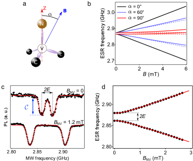
Focusing on weak magnetic field amplitudes, we consider that . The ESR frequencies are then simply given by
| (4) |
This formula can be used whenever the transverse component of the magnetic field is much smaller than mT. This is illustrated in Figure 5(b), where the prediction of Equation (4) is plotted in dotted lines together with the full calculation (solid lines). Obviously the approximate formula is relevant for field amplitudes in the range 0-2 mT, which is the range we address in this work. In addition, if , then can be neglected and the ESR frequencies become
| (5) |
as indicated in the main paper.
Experimentally, the ESR frequencies are inferred from the optically-detected ESR spectrum, i.e. the NV defect PL rate as a function of the MW frequency . Once normalized to unity, it can be expressed as
| (7) | |||||
where denotes a Gaussian function, is the ESR linewidth (FWHM) and its contrast. Two measured ESR spectra are shown in Figure 5(c) for a single NV defect attached to the AFM tip, together with data fitting using Equation (7). Varying enables us to verify Equation (4) experimentally, as illustrated in Figure 5(d). Note that the vanishing slope at very low magnetic fields – i.e. when – is responsible for the fact that in our dual-iso-B images, the iso-B lines corresponding to zero field are always wider that those corresponding to a non-zero field.
.2 Determining the orientation of the NV defect
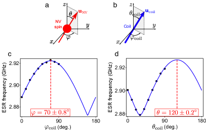
The orientation of the NV defect gives the projection axis of the measured magnetic field in all magnetometry experiments, i.e. . To determine the spherical angles and that characterize [Fig. 6(a)], we apply a calibrated magnetic field using a three-axis coil system [Fig. 6(b)] while monitoring one of the two ESR frequencies of the NV defect (e.g. ). The procedure we employed is as follows. We first set mT and , and sweep the angle from 0 to 90∘. This yields the angle by fitting Equation (4) to the data, using the fact that [Fig. 6(c)]. We next set and sweep from 0 to 90∘. The angle is deduced by fitting Equation (4) to the data, given that [Fig. 6(d)]. This procedure enables us to determine the angles and in the range , which completely defines the direction of .
.3 Magnetization and stray field simulations
The magnetization distribution inside the square film of Fe20Ni80 was computed using OOMMF softwareoommfbis . The parameters used for Fe20Ni80 were: spontaneous magnetization A/m and an exchange constant J/m. A magnetization cell size was used, which is below the micromagnetic exchange length in order to describe the vortex core structure precisely. From the calculated equilibrium magnetization [Fig. 7(a)], the stray magnetic field is computed by summing the contribution of all magnetization cells, and then projected along the NV defect axis in order to reach a map of . As an example, Figure 7(b) shows the calculated -axis component of the stray field for a probe-to-sample distance nm.
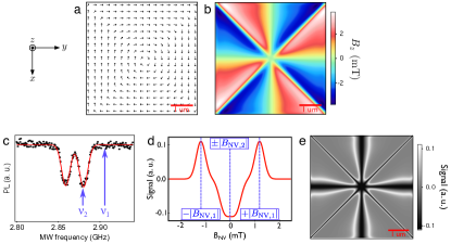
In the following, we take into account the strain-induced splitting, which was omitted in the main text for clarity purpose. We therefore use Equation (4) for the simulation of the magnetic field maps recorded with the scanning NV magnetometer. The dual-iso-B images shown in the main article are obtained by measuring the difference of NV defect PL intensity for two fixed MW frequencies and . The resulting signal reads
| (8) |
where is given by Equation (7). The signal is positive (resp. negative) when (resp. ) matches one of the two ESR frequencies – i.e. when (resp. ) – and is null otherwise.
As an illustration, we consider the same NV defect as in Figures 5(c)&(d), with an ESR spectrum at zero magnetic field reproduced in Figure 7(c). We choose MHz and MHz, which corresponds to mT and . Having fully characterized the ESR response, i.e. its linewidth and contrast, the resulting dual-iso-B signal can be computed as a function of , as shown in Figure 7(d). The simulated magnetic field maps are then obtained by applying the response to the calculated stray field once projected along the NV defect axis. An example of a calculated dual-iso-B image is shown in Fig. 7(e), where we assumed nm and the NV axis to be along the axis, i.e. .
.4 Distance dependence
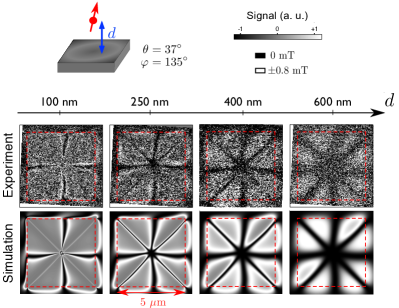
Magnetic field images recorded above a 5 m Fe20Ni80 square dot at several probe-to-sample distances, varying between and nm, are shown in Figure 8. For these experiments, the probe-to-sample distance is controlled by using the AFM in a dual-pass mode with a constant lift height during the second pass. The same NV defect probe as in Figure 3 of the main article is used, i.e. mainly oriented along the -axis. A good agreement with the simulations is found, which illustrates the three-dimensional stray field mapping capabilities of scanning NV magnetometry. The slight asymmetries observed in both the experimental and simulated images result from the imperfect alignment of the NV defect axis with respect to the -axis.
.5 Magnetic-field-induced fluorescence quenching
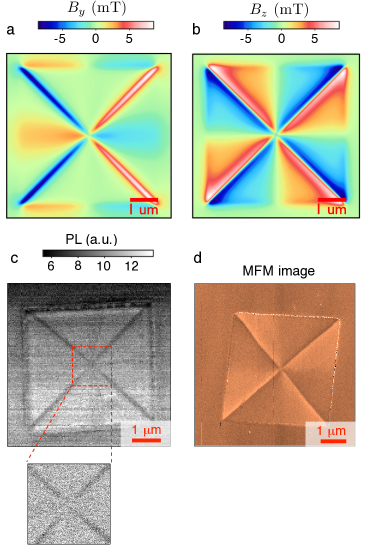
Although the simulations fairly agree with experimental data, the sharp structures lying along the square diagonals are not observed in the experimental image recorded at the smallest probe-to-sample distance nm [Fig. 8]. As explained in the main text, a strong stray field is generated by Néel domain walls in these regions. Indeed, the calculated magnetic field maps at nm indicate that the stray field components along the - and -axis reach nearly mT at the square diagonals, as illustrated in Figures 9(a)&(b). In this condition, the approximation is not fulfilled [see Eq. (2)] and the quantization axis is determined by the local magnetic field rather than by the NV defect axis. As a result, the spin projection along the NV axis is no longer a good quantum number and the eigenstates of the spin Hamiltonian are given by superpositions of the and spin sublevels Epstein2005 . In this regime, the contrast of optically detected ESR vanishes Tetienne2012bis . Magnetic field imaging through optically-detected ESR is therefore inefficient in the regime of ‘high’ off-axis magnetic field. This explains why the zero-field lines are not visible at the square’s diagonals for nm, where a strong off-axis magnetic field is experienced by the NV defect.
It was also shown that the decreased ESR contrast is accompanied by a reduction of the NV defect PL intensity when the magnitude of increases Epstein2005 ; Lai2009 . Such a magnetic-field-dependent PL can be exploited as an alternative method to map high off-axis magnetic field regions Rondin2012bis ; Tetienne2012bis . This is illustrated in Figure 9(c) where dark lines are observed along the square’s diagonals in the PL image for a probe-to-sample distance nm. In this experiment, we record the NV defect PL intensity without applying any MW field. The dark lines indicate a PL quenching induced by the off-axis component of the magnetic field generated by Néel domain walls. Near the center of the magnetic structure, the magnetic field amplitude decreases [see Fig. 9(c)], which enabled us to image the vortex core using the ESR response of the NV defect.
We note that the resulting PL quenching image exhibits obvious similarities with the one recorded with a magnetic force microscope (MFM), which is sensitive to the field gradient [Fig. 9(d)].
.6 Vortex polarity and chirality
The product of the vortex chirality and the vortex core polarity can be determined by simply examining the zero-field contours around the vortex core in the experimental dual-iso-B images. Indeed, zero-field lines separate the regions of positive and negative magnetic field projection. It is then possible to determine which “lobes” have the same sign as the vortex core field. Figure 10(a) shows the magnetic field map calculated at nm from the sample surface and projected along the -axis, for all possible combinations of and . As expected, the pairing of the zero-field contours around the vortex core (black dotted lines) are fixed by the product . Comparing the experimental results to simulations directly enables to determine that for the vortex state studied in Figure 3 of the main text [reproduced in Fig. 10(b)].
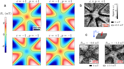
By applying an external magnetic field that cancels out the net field above the vortex core, the polarity of the vortex core can be determined as shown in the main paper. In Figures 10(c), we rather show dual-iso-B images obtained for a bias field antiparallel to the vortex core’s field such that is slightly positive or slightly negative. In the latter case, the net field above the vortex core is now of opposite sign compared to the zero-field case, which reverses the pairing of the zero-field lines in the image.
I Micromagnetic simulations for domain wall imaging
As indicated in the conclusion of the main manuscript, the direct quantitative measurement of weak magnetic fields, without perturbation and with a nanoscale resolution, may allow clearing some important issues in nanomagnetism. As an example, we show in this final section how scanning-NV magnetometry might allow to clearly identify the nature of magnetic domain walls (DW) in ultrathin ferromagnetic films with perpendicular anisotropy.
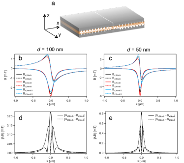
The magnetism of ultrathin films has attracted a renewed interest since the experimental discovery of the relevance of Dzyaloshinskii-Moriya interactions (DMI) in ultrathin magnetic films in contact with non magnetic layers Bode2007 . In particular, it has been shown that the DMI affects the nature of the lowest-energy magnetic domain wall structures in such films Thiaville2012bis , which in turn controls their current-induced motion Khvalkovskiy2013 . In the following, we present micromagnetic simulations of domain walls (DWs) in a thin film with perpendicular anisotropy, the typical sample being Pt/Co(0.6nm)/AlOx Miron2011 .
As shown in Figure 11(a), we consider a film parallel to the - plane, with a DW centered at that extends to infinity along the direction. The magnetization distribution in the case of a Bloch- and Néel-type DW was obtained using OOMMF software, from which the magnetic stray field was computed [Figure 11(b)&(c)] with typical probe-to-sample distances nm and nm. Figure 11(d)&(e) shows the absolute difference in the magnetic stray field produced by the two types of DWs at the same probe-to-sample distances. Obviously the calculated stray fields, reaching a few milliteslas right above the DW, are in the operation range of the NV magnetometer, and the % difference between the two types of DW is large enough to allow the NV magnetometer to experimentally determine the nature of the DW.
References
- (1) Donahue M. J. and Porter D. G. OOMMF User’s Guide, Version 1.0 Interagency Report NISTIR 6376, National Institute of Standards and Technology, Gaithersburg, MD http://math.nist.gov/oommf (1999).
- (2) Epstein, R. J., Mendoza, F. M., Kato, Y. K. & Awschalom, D. D. Anisotropic interactions of a single spin and dark-spin spectroscopy in diamond. Nature Phys. 1, 94-98 (2005).
- (3) Tetienne J.-P., Rondin L., Spinicelli P., Chipaux M., Debuisschert T., Roch J.-F. and Jacques V.,Magnetic-field-dependent Photodynamics of Single NV Defects in Diamond: An Application to Qualitative All-optical Magnetic Imaging. New J. Phys. 14 103033 (2012).
- (4) Lai, N. D., Zheng, D., Jelezko, F., Treussart F. & Roch, J.-F. Influence of a static magnetic field on the photoluminescence of an ensemble of nitrogen-vacancy color centers in a diamond single-crystal. Appl. Phys. Lett. 95, 133101 (2009).
- (5) Rondin L., Tetienne J.-P., Spinicelli P., Dal Savio C., Karrai K., Dantelle G., Thiaville A., Rohart S., Roch J.-F. and Jacques V., Nanoscale magnetic field mapping with a single spin scanning probe magnetometer, Appl. Phys. Lett. 100, 153118 (2012).
- (6) Bode, M. et al., Chiral magnetic order at surfaces driven by inversion asymmetry, Nature 447, 190 (2007).
- (7) Thiaville, A., Rohart, S., Jué, E., Cros, V., & Fert, A., Dynamics of Dzyaloshinskii domain walls in ultrathin magnetic films, Europhysics Lett. 100, 57002 (2012).
- (8) Khvalkovskiy, et al., Matching domain-wall configuration and spin-orbit torques for efficient domain-wall motion, Phys. Rev. B 87, 020402(R) (2013).
- (9) Miron, I. M. et al., Fast current-induced domain-wall motion controlled by the Rashba effect, Nat. Mater. 10, 419 (2011).