Spin mixing conductance at a well-controlled platinum/yttrium iron garnet interface
Abstract
A platinum (Pt)/yttrium iron garnet (YIG) bilayer system with a well-controlled interface has been developed; spin mixing conductance at the Pt/YIG interface has been studied. Crystal perfection at the interface is experimentally demonstrated to contribute to large spin mixing conductance. The spin mixing conductance is obtained to be at the well-controlled Pt/YIG interface, which is close to a theoretical prediction.
pacs:
75.40.Gb, 72.25.-b, 75.30.Ds, 75.76.+jSpin pumping enables a generation of an electric signal in the form of a spin current even in an insulator at room temperature kajiwara, Harri , which encourages efforts to develop a new class of insulator spintronics kajiwara, Harri ; Uchida Spinseebeck2 ; Qiu et al. (2012); wu et al. (2011); Sandweg et al. (2011); wu et al. (2012); Azevedo et al. (2013). The efficiency of the spin pumping is described in terms of spin mixing conductance at an interface. Improvement of spin mixing conductance is important for the development of spintronics devices kajiwara, Harri ; Uchida Spinseebeck2 ; Qiu et al. (2012); wu et al. (2011); Sandweg et al. (2011); wu et al. (2012); Azevedo et al. (2013); Hou et al. (2012); Ando et al. (2011, 2010); Uchida et al. (2008); Jaworski et al. (2010); Uchida et al. (2010). On the other hand, atomic structures at a metal/insulator interface have not been successfully observed or controlled thus far, and such situations can be the reason of scatter in the experimentally obtained values of spin mixing conductance.
To overcome this problem, we prepared a bilayer spin pumping system composed of a well-controlled single-crystalline yttrium iron garnet (YIG) surface covered with a platinum (Pt) film, and we studied the spin mixing conductance at the Pt/YIG interface in this study. This interface has been studied extensively because of the extremely small magnetic damping of YIG Geller et al. (1957); Cherepanov et al. (1993); Serga et al. (2010) and an effective spin current detector of Pt in the sense of the inverse spin Hall effect (ISHE) Saitoh et al. (2006); Azevedo et al. (2005).
Spin mixing conductance refers to the efficiency with which the spin currents across at the Pt/YIG interface are generated. In a model of spin pumping Tserkovnyak et al. (2002, 2002), the DC component of the generated spin current density, , in the Pt layer at the interface can be expressed as
| (1) |
where , , , , and are the angular frequency of magnetization precession, the Dirac constant, the real part of spin mixing conductance at the interface, the saturation magnetization of YIG, and the precessing magnetization in YIG, respectively. The expression is the component of . The axis is directed along the magnetization-precession axis. The spin current density can be detected as a voltage signal via ISHE in the Pt layer, which enables the experimental estimation of the spin mixing conductance Ando et al. (2008, 2011); Nakayama et al. (2011).
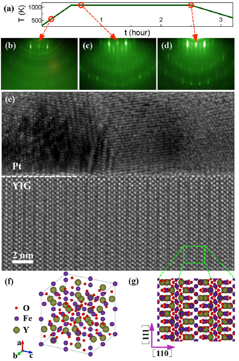
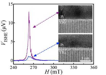
YIG films used in this work were grown on (111) gadolinium gallium garnet substrates by using a liquid phase epitaxy method in flux at the temperature of 1,210 K. The thickness of the YIG films was about 4.5 . We preformed annealing with an oxygen pressure of Torr (Fig. 1 (a)) to improve the crystal perfection of the YIG surface, or bombarded the YIG surface with accelerated ion beams to create an obvious amorphous layer (Insets to Fig. 2). 10 nm-thick Pt films were deposited on those YIG films using a pulse laser deposition system at room temperature in the same vacuum chamber.
reflection high energy electron diffraction (RHEED) was used to observe the surface structure of the YIG film during the annealing. The Pt/YIG interface structure was characterized by a high-resolution transmission electron microscopy (TEM). The crystalline characterization was carried out by using an X-ray diffraction (XRD) system and TEM. The lattice constant was calculated from the XRD and electron diffraction patterns. The saturation magnetization and the gyromagnetic ratio, were estimated by using the method described in Ando et al. (2008, 2011). Electrical conductivity of the Pt film was measured by using a four-probe method.
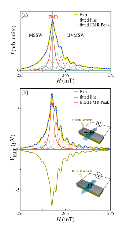
Spin pumping was measured by using an electron spin resonance system. The sample was placed near the center of a cavity, where the magnetic field component of the microwave mode is maximized and the electric-field component is minimized. A microwave with the frequency of =9.44 GHz was excited in the cavity. A static magnetic field was applied to the sample. The microwave absorption intensity and the ISHE voltage signal between the two electrodes attached to the Pt layer were measured at room temperature. The sign of reverses when the direction of the external magnetic field is reversed (Fig. 3 (b)), which is consistent with the spin pumping Tserkovnyak et al. (2002, 2002). Both and spectra are fitted by using multi-Lorentz functions (Fig. 3(b), (c)). The fitted peak positions and the full width at half maxima (FWHMs) of the spectrum are in a good agreement with the values obtained for the spectrum.
A change in the surface structure was observed in situ by RHEED using an electron beam along the [110] direction of the YIG surface. Diffraction patterns were recorded with a digital camera during the annealing (Figs. 1(b), (c), and (d)). Several halo rings along with the weak streak patterns were observed in the RHEED patterns at the beginning of annealing (Fig. 1(b)), which suggests that a thin polycrystalline layer exists on the YIG surface. For a higher annealing temperature, the halo rings disappeared as a result of the surface reintegration (Fig. 1(c)). After being annealed at 1073 K for 2 hours, sharp streak patterns appeared, and were prominent even in the first Laue zone (Fig. 1(d)). This implies that the annealed YIG has an atomically smooth surface with a single crystalline structure.
The cross-sectional structure of the prepared Pt/YIG interface was observed by a high-resolution TEM (Fig. 1(e)). the crystal perfection of the YIG surface was found to be well kept; the Pt/YIG interface was clear and a lattice-like contrast was observed even at the first several atomic layers at the YIG side in (Fig. 1(e)). The YIG layer has a cubic garnet structure, whose unit cell is shown in Fig. 1(f). A projection of the unit cell along the [112] direction is shown in Fig. 1(g). The lattice constant of the YIG film, determined by both ED and XRD, was 12.376 Å, which is in good agreement with the value found in literature Geller et al. (1957). On the other hand, the Pt layer showed a typical multi-crystalline structure without a preferred orientation. The lattice constant of the Pt layer was 3.92 Å, which is also in good agreement with the value reported in literature value Waseda et al. (1975). Such a well-controlled and well-defined Pt/YIG interface is a good reference for comparison with interfaces discussed in theoretical works.
Figure 2 shows ISHE voltage signal at a 20 mW microwave power for two Pt/YIG samples with different interface structures, which are shown in the insets to Fig. 2. One sample has a well-controlled Pt/YIG interface, while a nano-scale amorphous layer was formed at the Pt/YIG interface in another sample. The ISHE voltage signal observed in the sample with a bad interface decreased markedly compared to the ISHE voltage signal of the sample with a well-controlled interface. Because the Pt layers of the two samples were prepared under the same conditions with the same thickness, the decrease in can be attributed to the Pt/YIG interface condition; the thin amorphous layer blocks the efficient spin exchange between Pt and YIG and decreases spin mixing conductance (Eq. 1). This result suggests that a better quality interface is necessary for larger spin mixing conductance.
Figure 3 shows the observed spectra of microwave absorption intensity and ISHE voltage signal at 10 mW microwave power of a sample with a well-controlled Pt/YIG interface. One advantage of a good interface structure is that it allows, not only but also spectra, a clear separation of spectral contributions from different spin wave modes, e.g. magnetostatic surface spin wave, backward volume magnetostatic spin wave, and ferromagnetic resonance (FMR) modes (Figs. 3(a) and (b)). The Gibert damping constant can be estimated from FWHM of a FMR absorption peak as , where is the gyromagnetic ratio. The value of was calculated to be from for the FMR mode.
The spin current density, gererated by the FMR excitation, is estimated to be at 10 mW microwave power in the Pt/YIG system by using the following equation Ando et al. (2011); Nakayama et al. (2011):
| (2) |
Here, , , , , and are, respectively, the distance between the two electrodes of the sample, the thickness, the electric conductivity, the spin Hall angle, and the spin diffusion length of Pt. The quantities , , and were measured to be 1.5 mm, 10 nm, and . We used a literature value to set 7.7 nm Nakayama et al. (2011). The spin Hall angle of the Pt film was estimated to be 0.012 by using a Pt/permalloy bilayer spin pumping system, in which the Pt layer was prepared under the same conditions as the Pt/YIG samples and had the same thickness as them. Ando et al. (2011); Nakayama et al. (2011). The induced by the FMR excitation was estimated to be at 10 mW microwave power (Fig. 3(b)).
By using the Landau-Lifshitz-Gilbert equation, Eq. 1 yields
| (3) |
where is the amplitude of the microwave magnetic field. In this work, T, , , and . We estimated the spin mixing conductance as at the Pt/YIG interface, which is close to a theoretical prediction by Jia et al.xiao et al. (2011).
In summary, we prepared a single crystalline YIG surface covered with a Pt film and studied its spin mixing conductance, which governs the spin pumping efficiency at the interface. Crystal perfection is experimentally demonstrated to contribute to a large spin mixing conductance. With a well-controlled interface, the spin mixing conductance of a Pt/YIG interface reached the value of , which is close to a theoretical prediction. This work provides an explicit guideline for pursuing large spin mixing conductance at metal/insulator interfaces.
This work was supported by Fundamental Research Grants from CREST-JST “Creation of Nanosystems with Novel Functions through Process Integration”; NEXT from the cabinet office, Japan, a Grant-in-Aid for Scientific Research (A) (21244058); PRESTO-JST ”Phase Interfaces for Highly Efficient Energy Utilization” all from MEXT, Japan.
References
- (1) Y. Kajiwara, K. Harii, S. Takahashi, J. Ohe, K. Uchida, M. Mizuguchi, H. Umezawa, H. Kawai, K. Ando, K. Takanashi, S. Maekawa, and E. Saitoh, Nature 464, 262 (2010).
- (2) K. Uchida, J. Xiao, H. Adachi, J. Ohe, S. Takahashi, J. Ieda, T. Ota, Y. Kajiwara, H. Umezawa, H. Kawai, G. E. W. Bauer, S. Maekawa, and E. Saitoh, Nature Mater. 9, 894 (2010).
- Sandweg et al. (2011) C. W. Sandweg, Y. Kajiwara, A. V. Chumak, A. A. Serga, V. I. Vasyuchka, M. B. Jungfleisch, E. Saitoh, and B. Hillebrands, Phys. Rev. Lett. 106, 216601 (2011).
- wu et al. (2011) B. Heinrich, C. Burrowes, E. Montoya, B. Kardasz, E. Girt, Y.-Y. Song, Y. Sun, and M. Wu, Phys. Rev. Lett. 107, 066604 (2011).
- wu et al. (2012) C. Burrowes, B. Heinrich, B. Kardasz, E. A. Montoya, E. Girt, Y. Sun, Y. Song, and M. Wu, Appl. Phys. Lett. 100, 092403 (2012).
- Azevedo et al. (2013) S. M. Rezende, R. L. Rodriguez-Suarez, M. M. Soares, L. H. Vilela Leao, D. Ley Dominguez, and A. Azevedo, Appl. Phys. Lett. 102, 012402 (2013).
- Qiu et al. (2012) Z. Qiu, Y. Kajiwara, K. Ando, Y. Fujikawa, K. Uchida, T. Tashiro, K. Harii, T. Yoshino, and E. Saitoh, Appl. Phys. Lett. 100, 022402 (2012).
- Hou et al. (2012) Dazhi Hou, Z. Qiu, K. Harii, Y. Kajiwara, K. Uchida, Y. Fujikawa, H. Nakayama, T. Yoshino, T. An, K. Ando, Xiaofeng. Jin, and E. Saitoh, Appl. Phys. Lett. 101, 042403 (2012).
- Ando et al. (2011) K. Ando, S. Takahashi, J. Ieda, H. Kurebayashi, T. Trypiniotis, C. H. W. Barnes, S. Maekawa, and E. Saitoh, Nature Mater. 10, 655 (2011).
- Ando et al. (2010) K. Ando, M. Morikawa, T. Trypiniotis, Y. Fujikawa, C. H. W. Barnes, and E. Saitoh, Appl. Phys. Lett. 96, 082502 (2010).
- Uchida et al. (2008) K. Uchida, S. Takahashi, K. Harii, J. Ieda, W. Koshibae, K. Ando, S. Maekawa, and E. Saitoh, Nature 455, 778 (2008).
- Jaworski et al. (2010) C. M. Jaworski, J. Yang, S. Mack, D. D. Awschalom, J. P. Heremans, and R. C. Myers, Nature Mater. 9, 898 (2010).
- Uchida et al. (2010) K. Uchida, H. Adachi, T. Ota, H. Nakayama, S. Maekawa, and E. Saitoh, Appl. Phys. Lett. 97, 172505 (2010).
- Geller et al. (1957) S. Geller, and M. A. Gilleo, Acta Crystallogr. 10, 239 (1957).
- Cherepanov et al. (1993) V. Cherepanov, I. Kolokolov, and V. L’vov, Phys. Rep. 229, 81 (1993).
- Serga et al. (2010) A. A. Serga, A. V. Chumak, and B. Hillebrands, J. Phys. D: Appl. Phys. 43, 264002 (2010).
- Saitoh et al. (2006) E. Saitoh, M. Ueda, H. Miyajima, and G. Tatara, Appl. Phys. Lett. 88, 182509 (2006).
- Azevedo et al. (2005) A. Azevedo, L. H. Vilela Leao, R. L. Rodriguez-Suarez, A. B. Oliveira, and S. M. Rezende, J. Appl. Phys. 97, 10C715 (2005).
- Tserkovnyak et al. (2002) Y. Tserkovnyak, A. Brataas, and G. E. W. Bauer, Phys. Rev. Lett. 88, 117601 (2002).
- Tserkovnyak et al. (2002) Y. Tserkovnyak, A. Brataas, and G. E. W. Bauer, Phys. Rev. B 66, 224403 (2002).
- Ando et al. (2008) K. Ando, Y. Kajiwara, S. Takahashi, S. Maekawa, K. Takemoto, M. Takatsu, and E. Saitoh, Phys. Rev. B 78, 014413 (2008).
- Ando et al. (2011) K. Ando, S. Takahashi, J. Ieda, Y. Kajiwara, H. Nakayama, T. Yoshino, K. Harii, Y. Fujikawa, M. Matsuo, S. Maekawa, and E. Saitoh, J. Appl. Phys. 109, 103913 (2011).
- Nakayama et al. (2011) H. Nakayama, K. Ando, K. Harii, T. Yoshino, R. Takahashi, Y. Kajiwara, K. Uchida, Y. Fujikawa, and E. Saitoh, Phys. Rev. B 85, 144408 (2012).
- Waseda et al. (1975) Y. Waseda, K. Hirata, and M. Ohtani, High Temp. High Pressures 7, 221 (1975).
- xiao et al. (2011) X. Jia, K. Liu, K. Xia, and G. E. W. Bauer, Europhys. Lett. 96, 17005 (2011).
A list of figures
-
1.
(a) The annealing process for YIG films. (b), (c), and (d) are the RHEED patterns of a YIG surface at different stages of the annealing. (e) A cross-sectional high-resolution TEM image of a Pt/YIG interface, of which YIG was annealed as the process shown in (a). (f) The unit cell of the cubic garnet (space group Ia3d). (g) A projection of the cubic garnet unit cell along the [210] direction.
-
2.
The external magnetic field dependence of the inverse spin Hall voltage signal of Pt/YIG samples at 20 mW microwave power. Cross sectional images by TEM are shown as insets. The upper sample with a well-controlled Pt/YIG interface, while a nano-scale amorphous layer was formed at the Pt/YIG interface in the lower sample.
-
3.
(a) The external magnetic field dependence of the microwave absorption intensity and the multi-Lorentz fitting results of a Pt/YIG sample with a well-controlled Pt/YIG interface at 10 mW microwave power. (b) The external magnetic field dependence of the inverse spin Hall voltage . Insets to (b) are schematic illustrations of the spin pumping experimental setting for and , of which the external magnetic fields are in the opposite direction. The multi-Lorentz fitting result of spectrum for is shown.


