Quantum interference hybrid spin-current injector
Abstract
We propose a quantum interference spin-injector nanodevice consisting of a superconductor-normal metal hybrid loop connected to a superconductor-ferromagnet bilayer via a tunneling junction. We show that for certain values of the applied voltage bias across the tunnel barrier and the magnetic flux through the loop the spin-current can be fully polarized. Moreover, by tuning the magnetic flux one can switch the sign of the spin polarization. This operation can be performed at frequencies within the tens of GHz range. We explore the nanodevice in a wide range of parameters, establish the optimum conditions for its experimental realization and discuss its possible applications.
pacs:
72.25.-b,85.75.-d,74.50.+rINTRODUCTION.- Generation of strongly spin-polarized currents and their control in nanoscale circuits is highly desirable in the field of spintronics Zutic . In this context, there have been a number of proposals to achieve highly spin-polarized currents using different nanodevices Stefanski ; Csonka ; Feng ; Zozoulenko ; Chen ; Giazotto2003 . Such a spin-currents can produce a dynamical switching by means of spin-transfer torque Slonczewski ; Berger of the magnetization in multilayer ferromagnetic structuresBuhrman . Such a switching procedure is used in magnetic random access memories, where the magnetic configuration is controlled by spin-polarized currents. Usually, the source of spin-polarized currents is a ferromagnet with highly-polarized conduction electrons. Therefore, materials with half-metallic behavior, as for example CrO2, are ideal candidates for spin-injectors. However, their growth in hybrid nano circuits still remains a challenge. Alternatively, strongly spin-polarized currents can be created in hybrid structures consisting of a superconductor (S) and a ferromagnetic (F) layer Nazarov2002 ; Giazotto2008 tunnel-coupled to a normal metal (N). It was shown that in such hybrid structures fully spin-polarized currents can be induced. In particular, the NISF structure (I denotes an insulating layer) studied in Ref. Giazotto2008 allows for tuning of the sign and magnitude of the spin polarization by changing the bias voltage.
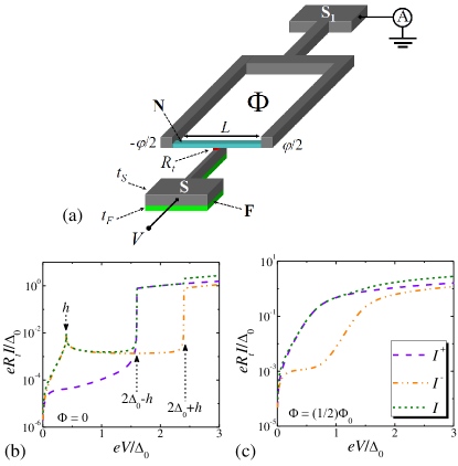
Here, we propose a spintronic nanodevice that, on the one hand, is able to provide strongly spin-polarized currents, and on the other hand allows for a switching of the current polarization not only by means of a voltage bias but also by an external magnetic flux. The switching time between positive and negative current polarization can be achieved in the nanosecond range or faster. The device consists of a superconducting loop (S1) interrupted by a N wire of length . In addition, a SF bilayer is tunnel-coupled to N through a junction with normal-state resistance [see Fig. 1(a)]. We assume (i) a good contact between the S and F layers and (ii) that is much larger than the SF contact resistance which ensures the bilayer to be in local equilibrium. () labels the S (F) layer thickness, and the SF bilayer is kept at a constant voltage , while the other end of the structure is grounded. Except for the F layer, the setup shown in Fig. 1(a) resembles the ones investigated in recent experiments on hybrid nanostructures Giazotto2010 ; Meschke .
Our hybrid interference spin-current injector operates as follows: by applying a voltage bias a finite quasiparticle current flows through the structure. The amplitude of the resulting current depends on the density of states (DoS) of both the SF bilayer and the N wire. The former shows a Zeeman-splitting induced by the exchange field of the F layer, whereas the latter is modified by the proximity effect induced from the nearby contacts with the S1 loop. As it is shown below, the current flowing through the structure can be strongly spin-polarized. In addition to the dc voltage bias, the device can also be operated by an externally-applied magnetic flux. By neglecting the loop inductance, the magnetic flux fixes the superconducting phase difference across the SN boundaries according to , where is the flux quantum. Since the DoS in the N wire depends on the phase difference Belzig , by varying the magnetic flux through the loop one can modify the DoS in N and, in turn, the electric current and its spin-polarization. Therefore, our device can be used as a phase-tunable spin-injector. One of the advantages of our setup with respect to a voltage tunable spin-injector based on the results of Refs. Nazarov2002 ; Giazotto2008 is that the switching speed provided by the magnetic flux allows, in principle, for a much higher operation frequency.
THE MODEL.-In order to model the spin-current injector we consider a SF system which may consists either of two thin S and F layers in good electric contact, or of a superconducting layer in contact with a ferromagnetic insulator. In particular, we consider the situation where the thickness of the S layer is smaller than the superconducting coherence length, and the F thickness is smaller than the length of the condensate penetration into the ferromagnet. In such a case the ferromagnet induces a homogeneous effective exchange field () in S through proximity effect which modifies the superconducting gap (). and the effective gap in S () are given by and , respectively, where is the original exchange field existing in the ferromagnetic layer and () is the normal-state DoS in S (F) at the Fermi energy. If and for it follows that while . The effect of on the superconductor leads to a spin-dependent BCS-like DoS shifted by the effective exchange energy (similarly to what happens for a Zeeman-split superconductor in a magnetic field) Bergeret2001 ; Bergeret2012 ; Meservey1 ; Meservey2 . The total DoS of the SF layer is then given by the sum of the spin-up () and spin-down () density of states which can be written as Meservey1 ; Meservey2
| (1) |
where is the energy measured from the condensate chemical potential, and is the temperature. The effective superconducting order parameter, , depends on both the temperature and the magnitude of the exchange field, and has to be determined self-consistently from the gap equation , where , is the zero-temperature order parameter in the absence of exchange field, is the superconducting critical temperature, is the Boltzmann constant, and is the Debye frequency. The parameter in Eq. (1) accounts for the inelastic scattering energy rate within the relaxation time approximation Dynes1984 ; Pekola2004 . Tunneling conductance measurements on SIS junctions Moodera1990 , where I is a ferromagnetic insulator, have shown the accuracy of the description of the DoS provided by Eq. (1).
We assume that the tunnel junction between the SF bilayer and the normal metal is situated in the middle of the N wire, and that the resistance of the tunneling contact is much larger than the normal-state resistance of the N wire and the resistance of the SN interfaces. Therefore, the voltage drop occurs entirely at the SF/N contact. Moreover, we assume the wire transverse dimensions to be much smaller than , so that it can be considered as quasi-one-dimensional (1D), and neglect any spatial later extension of the tunnel junction footnote . For the sake of clarity in our analysis we choose identical superconductors S and S1 for the nanodevice of Fig 1(a).
The total quasiparticle current is given by the sum of the spin-up and spin-down contributions, where
| (2) | |||||
is the DoS in the middle of the N wire, and is the electron charge. The exact form of can be obtained from the knowledge of the retarded quasiclassical Green’s function. The latter is the solution of the 1D Usadel equation in the N region usadel
| (3) |
where is a 22 matrix in the Nambu space, is the Thouless energy and is the diffusion constant in N. All lengths are given in units of . The DoS in the normal wire is then determined by the real part of the (1,1) component of . It is known that due to the proximity effect shows a minigap whose size depends, among other parameters, on the phase difference across the N wireGiazotto2010 ; Meschke ; Cuevas2007 ; Saclay . Thus, by varying the magnetic flux through the loop one can control the size of the minigap in N, which is maximized for and vanishes for , where is an integer.
Equation (3) is supplemented by boundary conditions describing the transmissivity of the SN interfaces KL
| (4) |
where , and are the bulk BCS Green’s functions. For simplicity we have assumed that the normal-state conductivity of the S and N parts of the wires are the same. We notice that in the case of a perfectly-transmissive SN interface, , and Eq. (4) imposes the continuity of at the boundary. Furthermore, we neglect the suppression of the order parameter in S1 at the NS1 boundaries due to inverse proximity effect Saclay ; cuevas . We expect however this effect to be very small in a real nanostructure by making the cross section of the loop much larger than that of the N wire. Finally, in all the following calculations we set as a representative value describing realistic tunnel junctions Pekola2004 .
RESULTS AND DISCUSSION.- We first consider the case of a short N bridge satisfying the condition , and assume perfectly-transmissive SN contacts. In this regime the spin-current injector performance is optimized since the proximity effect in N is maximized. In this case the DoS in the middle of the wire can be obtained analytically, Heikkila2002
| (5) |
It has a BCS-like form with an effective gap, , whose magnitude depends on the magnetic flux . In particular for the minigap is completely closed. Substituting Eqs. (1,5) into the expression for the current, Eq. (2), we compute the spin-currents . The voltage dependence of and of the total current through the device are shown in Figs. 1(b) and 1(c) for zero and half-integer flux quantum, respectively. Within certain ranges of voltage, the spin-up and spin-down currents can differ by several orders of magnitude. In the zero flux case [see Fig. 1(b)], the spin-down current dominates the transport () if , whereas for the opposite occurs (). The thresholds for the onset of large quasiparticle current [see panel (b)] correspond to the sum of the gaps on both sides of the barrier (), i.e., in the SF and in the N layer. This is in analogy to the quasiparticle I-V characteristic of a conventional SIS tunnel junction Tinkham . We note that a Josephson supercurrent, although pretty small, can flow through the deviceGiazotto2010 ; Meschke ; Giazotto2011 , however in our case a spin-polarized current is achieved only if a finite bias voltage (i.e., ) is applied. For half-integer flux quantum values [see Fig. 1(c)] the behavior is modified, i.e., is substantially larger than in the whole range of voltage. As a consequence, it turns out that by applying a magnetic flux through the loop the voltage dependence of the current polarization, defined as
| (6) |
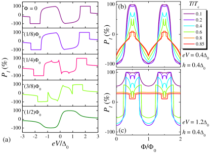
may change drastically. This is shown explicitly in Fig. 2(a) where the dependence is plotted for different values of the applied flux at and . We emphasize that high spin polarization of both signs (i.e., up to ) can be achieved in the nanostructure within suitable voltage bias windows and magnetic flux.
We demonstrate in this way that, in addition to the voltage dependent switching of the current-polarization, our device is able to switch the magnitude and sign of by tuning the magnetic flux through the loop. In Figs. 2(b) and 2(c) we show the dependence for two different values of the voltage bias at different temperatures. The maximum values of are typically achieved at low temperatures, , where the current is almost full-polarized. We stress, however, that even for temperatures up to a sizeable polarization switching effect is still observable.
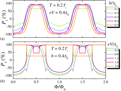
In Fig. 3 we show the flux dependence of the current spin polarization calculated at for different values of the effective exchange field in the SF structure [panel (a)], and for different voltage bias applied across the junction [panel (b)]. From these figures it follows that strong spin-polarized currents and sign switching (i.e., around ) can be achieved for large enough values of and subgap voltages. Large values of can also be achieved for , though the sign switching is not possible for such large bias [see Fig. 3(b)].
All the results presented above have been obtained in the limit of a short N wire, i.e., when , and for perfectly-transmitting SN interfaces. In the case of an arbitrary Thouless energy (i.e., for arbitrary wire length) and arbitrary transparency of the SN interfaces we have solved numerically Eqs. (3-4) in the N region for the retarded Green’s function to obtain the DoS in the middle of the wire, and computed the currents from Eq. (2). In Fig. 4 we show the results for the dependence of the current spin-polarization on the magnetic flux. Panel (a) shows this dependency for different Thouless energies and a highly-transparent SN interface () assuming . One can see that by increasing the length , i.e., by decreasing , the range of switching is suppressed. Nevertheless, a large spin polarization modulation amplitude is still present up to . By choosing, for instance, aluminum (Al) with eV and silver (Ag) with m2s-1 as prototypical materials to implement the spin-current injector, this value would correspond to a realistic length of N wire, nm. It is easily understandable that if the wire is very long, i.e., for , the proximity effect in the middle of the N region is strongly weakened with the consequences that the DoS is almost magnetic-flux independent, and the spin polarization does not show any significant changes as a function of . We stress, however, that even in the case of a long wire the achievable current polarization may be strong providing a proper choice of the bias voltage [see, for example, the blue curve in Fig. 4(a)].
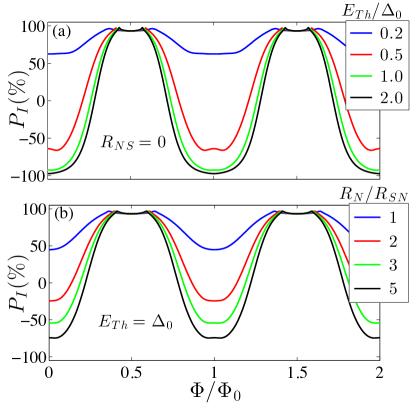
A finite interface resistance at the SN contact has a similar effect on the magnitude and modulation amplitude of the spin-polarization. According to Eq. (4) the strength of the proximity effect is related to the coefficient . For a highly-transparent SN interface () the proximity effect in the wire is maximized, and in turn the modulation of the DoS in the metal. For finite values of , the suppression of the proximity effect leads to a weaker dependence of the DoS on the magnetic flux and, accordingly, the switching effect is suppressed. This is shown in Fig. 4(b), where the dependence is plotted for different values of at and . It can be seen that by decreasing the switching occurs within a smaller range of . We note again, that even for of the order of , large values can be achieved as well for proper applied magnetic fluxes [see the blue curve in Fig. 4(b)].
The switching of is therefore optimized by having highly-transparent SN interfaces, and for intermediate-length or short N wires (i.e., ). In general, tuning of the phase bias in the structure can be achieved experimentally through an integrated superconducting coil providing a suitable magnetic flux which allows, in principle, high-frequency operation. In this context, the characteristic polarization switching frequency is given by , i.e., it is determined by the minimum among the inverse time that the DoS requires to follow a change in the phase difference across the N wire, the characteristic frequency of the LC phase biasing circuit (where denotes the inductance and is the total capacitance), and the characteristic frequency of the superconductor. As Hz for intermediate-length N wires, can therefore easily approach values as high as Hz for suitable and parameters. By contrast, switching the spin polarization by changing the voltage bias across the tunnel junction is normally much slower. In such a case, can be estimated to be of the order of therefore yielding at most Hz as the relevant switching frequency achievable in a typical cryogenic setup.
We finally discuss two conditions required for a correct operation of the spin-current injector: (i) The avoidance of magnetic hysteresis, and (ii) the occurrence of a good phase biasing in the structure. The first condition imposes that Tinkham , where is the Josephson supercurrent circulating along the loop, and is the ring geometric inductance. Condition (ii) ensures that the phase difference set by the magnetic flux drops entirely at the wire ends, allowing a full modulation of its DoS. This condition can be expressed as Meschke ; Saclay , where is the ring kinetic inductance Tinkham and is the loop normal-state resistance, while is the wire kinetic inductance. Experiments have shown that both conditions can be fulfilled by a proper choice of materials and a suitable geometry Meschke ; Saclay .
CONCLUSIONS.- In conclusion, we have proposed a hybrid quantum interference nanodevice that can be used as an efficient spin-current injector with controllable degree of current polarization. The device operates by combining phase-dependent superconducting proximity effect and an effective Zeemann splitting of the density of states induced by a ferromagnetic layer. Under optimal conditions it can provide strongly polarized (i.e., up to ) spin-up and spin-down currents in two ways: either by tuning an externally-applied magnetic flux or by changing the voltage bias across the structure. In the former case, switching frequencies of the order of tens of GHz can be achieved. Conventional metals combined with ferromagnetic insulators such as, for instance, Eu chalcogenides layers Moodera1990 ; Santos ; Miao appear as promising materials for the implementation of this proposal.
ACKNOWLEDGEMENTS.- F.G. acknowledges the FP7 program No. 228464 MICROKELVIN, the Italian Ministry of Defense through the PNRM project TERASUPER, and the Marie Curie Initial Training Action (ITN) Q-NET 264034 for partial financial support. The work of F.S.B was supported by the Spanish Ministry of Economy and Competitiveness under Project FIS2011-28851-C02-02. F.S.B thanks Prof. Martin Holthaus and his group for their kind hospitality at the Physics Institute of the Oldenburg University.
References
- (1) I. utić, J. Fabian, and S. Das Sarma, Rev. Mod. Phys. 76, 323 (2004).
- (2) P. Stefański, Phys. Rev. B 77, 125331 (2008).
- (3) S. Csonka, I. Weymann, and G. Zarand, Nanoscale 4, 3635 (2012).
- (4) X. Y. Feng, J. H. Jiang, and M. Q. Weng, Appl. Phys. Lett. 90, 142503 (2007).
- (5) I. V. Zozoulenko and M. Evaldsson, Appl. Phys. Lett. 85, 3136 (2004).
- (6) Z. Chen, B. Wang, D. Y. Xing, and J. Wang, Appl. Phys. Lett. 85, 2553 (2004).
- (7) F. Giazotto, F. Taddei, R. Fazio, and F. Beltram, Appl. Phys. Lett. 82, 2449 (2003).
- (8) E. B. Myers, D. C. Ralph, J. A. Katine, R. N. Louie and R. A. Buhrman, Science 285, 867 (1999).
- (9) J. C. Slonczewski, J. Magn. Mater. 159, L1 (1996).
- (10) L. Berger, Phys. Rev. B 54, 9353 (1996).
- (11) Daniel Huertas-Hernando, Yu. V. Nazarov, and W. Belzig, Phys. Rev. Lett. 88, 047003 (2002).
- (12) F. Giazotto and F. Taddei, Phys. Rev. B 77, 132501 (2008) .
- (13) F. Giazotto, J. T. Peltonen, M. Meschke, and J. P. Pekola, Nature Phys. 6, 254 (2010).
- (14) M. Meschke, J. T. Peltonen, J. P. Pekola, and F. Giazotto, Phys. Rev. B 84, 214514 (2011).
- (15) W. Belzig, F. K. Wilhelm, C. Bruder, G. Schön, and A. D. Zaikin, Superlatt. Microstruct. 25, 1251 (1999).
- (16) F. S. Bergeret, A. F. Volkov, and K. B. Efetov, Phys. Rev. Lett. 86, 3140 (2001).
- (17) F. S. Bergeret, A. Verso, and A. F. Volkov, Phys. Rev. B 86, 214516 (2012).
- (18) R. Meservey and P. M. Tedrow, Phys. Rep. 238, 173 (1994).
- (19) R. Meservey, P. M. Tedrow, and P. Fulde, Phys. Rev. Lett. 25, 1270 (1970).
- (20) R. C. Dynes, J. P. Garno, G. B. Hertel, and T. P. Orlando, Phys. Rev. Lett. 53, 2437 (1984).
- (21) J. P. Pekola, T. T. Heikkilä, A. M. Savin, J. T. Flyktman, F. Giazotto, and F. W. J. Hekking, Phys. Rev. Lett. 92, 056804 (2004).
- (22) X. Hao, J. S. Moodera, and R. Meservey, Phys. Rev. B 42, 8235 (1990).
- (23) F. Giazotto and F. Taddei, Phys. Rev. B 84, 214502 (2011).
- (24) As shown in Ref. Giazotto2011 , the product , depends very weakly on the spatial extension of the tunneling contact.
- (25) K. Usadel, Phys. Rev. Lett. 25, 507 (1970).
- (26) M. Yu. Kupriyanov and V. F. Lukichev, Zh. Exp. Teor. Fiz. 94,139 (1988) [Sov. Phys. JETP 67, 1163 (1988)].
- (27) J. C. Hammer, J. C. Cuevas, F. S. Bergeret, and W. Belzig, Phys. Rev. B 76, 064514 (2007).
- (28) H. le Sueur, P. Joyez, H. Pothier, C. Urbina, and D. Esteve, Phys. Rev. Lett. 100, 197002 (2008).
- (29) J. C. Cuevas, J. Hammer, J. Kopu, J. K. Viljas, and M. Eschrig, Phys. Rev. B 73, 184505 (2007).
- (30) T. T. Heikkilä, J. Särkkä, and F. K. Wilhelm, Phys. Rev. B 66, 184513 (2002).
- (31) M. Tinkham, Introduction to Superconductivity, 2nd ed. (McGraw-Hill, New York, 1996).
- (32) T. Santos, J. Moodera, K. Raman, E. Negusse, J. Holroyd, J. Dvorak, M. Liberati, Y. idzerda, and E. Arenholz, Phys. Rev. Lett. 101, 147201 (2008).
- (33) G.-X. Miao, M. Müller, and J. S. Moodera, Phys. Rev. Lett. 102, 076601 (2009).