A hybrid metal/semiconductor electron pump
for quantum metrology
Abstract
Electron pumps capable of delivering a current higher than 100 pA with sufficient accuracy are likely to become the direct mise en pratique of the possible new quantum definition of the ampere. Furthermore, they are essential for closing the quantum metrological triangle experiment which tests for possible corrections to the quantum relations linking and , the electron charge and the Planck constant, to voltage, resistance and current. We present here single-island hybrid metal/semiconductor transistor pumps which combine the simplicity and efficiency of Coulomb blockade in metals with the unsurpassed performances of silicon switches. Robust and simple pumping at 650 MHz and 0.5 K is demonstrated. The pumped current obtained over a voltage bias range of 1.4 mV corresponds to a relative deviation of 5 from the calculated value, well within the 1.5 uncertainty of the measurement setup. Multi-charge pumping can be performed. The simple design fully integrated in an industrial CMOS process makes it an ideal candidate for national measurement institutes to realize and share a future quantum ampere.
I INTRODUCTION
Linking measurement units to quantum effects rather than artefacts is a major achievement of modern scienceFlowers2004 . The electrical base unit of the S.I., the ampere, which is defined by the force acting between two ideal conductors, is not directly realized anymore. Instead, electrical metrology has been based since 1990 on voltage and resistance realized with the Josephson and quantum Hall effects Taylor1989 . For the S.I. to fully benefit from their remarkable accuracy, a full set of quantum electrical units based on and the Planck constant could be adopted, where the ampere would be a number of elementary charges per unit time. Just like the speed of light was fixed when the meter was redefined, the fundamental constants and would then be fixed and the of the new definition of the ampere would be made by using the combination of the Josephson and quantum Hall effects. A SET current standard based on an electron pump driven at a frequency , producing a quantized current (where is an integer) with an amplitude of 100 pA or more could also be used for the realization of the new ampere. Furthermore, such a current is necessary for the quantum metrological triangle experiment which consists in achieving Ohm’s law between the three effects used in quantum electrical metrology: Josephson effect (voltage), quantum Hall effect (resistance) and single electron tunneling effect (current). It aims to test the possible corrections to the relations linking and to the constants associated with three quantum effects: Josephson constant , von Klitzing constant and an estimate of the electron charge Piquemal2000 ; Keller2008 .
The understanding of the Coulomb blockade phenomenon Grabert1992 rapidly led to the design of electron pumps and turnstiles both with fixed Geerligs1990 ; Pothier1992 and tunable barriers Kouwenhoven1991 . While turnstiles require a bias voltage to operate, pumps deliver a d.c. current even at zero bias. Metallic pumps with fixed height tunnel oxide barriers and multiple Coulomb islands reached a relative accuracy in the 10-8 range, with up to 6 islands in series between 7 tunnel junctions Keller1996 ; Keller1999 . Their complex operation was simplified by using only 3 junctions while lowering errors due to cotunneling with resistors Lotkhov2001 . Despite these efforts the level of current remained below 10 pA (60 MHz), too small by at least one order of magnitude for a practical current source. They are also restricted to very low temperatures (below 50 mK) and cannot accept a bias voltage without a severe degradation of their accuracy Jehl2003 . With silicon technology, we previously demonstrated electron pumping in a device with two coupled islands and fixed barriers Pierre2010 . Hybrid normal/superconducting turnstiles Pekola2008 (which require a finite bias ) based on fixed barriers are also relatively slow but can be operated in parallel to increase the current Maisi2009 . An alternative option using optically driven self-assembled quantum dots has also been demonstrated recently Nevou2011 . A different pumping scheme revived a strong interest in the field because it reached the desired level of current Blumenthal2007 ; Fujiwara2008 ; Kaestner2008 ; Giblin2010 and recently an accuracy approaching the ppm level Giblin2012 . It uses non-adiabatic effects in the population of a dynamical quantum dot Kashcheyevs2010 . Operation in series of several such pumps have also been realized, with an integrated charge sensing scheme Fricke2011 . At the same time as metallic pumps with fixed barriers an experiment was performed which also uses orthodox Coulomb blockade but on a single semiconducting island connected by two tunable barriers Kouwenhoven1991 . Using phase shifts on the two barriers, quantized currents were obtained, up to 20 MHz. Although this pioneering work focuses on turnstile operation, electron pumping at zero bias was also briefly shown and discussed at the end of the report Kouwenhoven1991 . Later on, a similar experiment with a silicon device Ono2003 reached =1 MHz, and more recently the same idea was used but with -shift only, resulting again in turnstile operation Chan2011 .
In this work we clarify this pumping mechanism with a novel type of electron pumps using industrial silicon technology. We show that the phase difference between the sinewaves applied to the two tunable barriers determine the number of electrons pumped per cycle and the direction of the current. A convincing evidence that this pumping mechanism is at play is the observation of an odd/even behaviour depending on the position of the working point with respect to the Coulomb peaks of the device. Since the pump studied here shows that it is possible to combine orthodox Coulomb blockade and high speed, it opens new opportunities for quantum metrology. This article is organized as follows. In section II, the samples technology and main characteristics are presented briefly, together with the results of d.c. electrical transport which unveil their electrostatic properties. Section III describes the pumping principle and the experimental results, and section IV focuses on experiments designed to assess the stability and accuracy of the pump.
II SAMPLE DESIGN AND d.c. TRANSPORT
II.1 Fully-depleted silicon-on-insulator technology
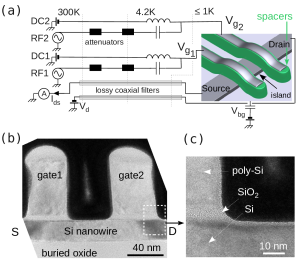
A difficulty with quantized current sources comes from the necessity to have a system containing at some point a well defined number of charges . Whether this relies on a high charging energy for metallic dots (here is the total capacitance of the island), or on the one-particle energy level spacing in a confinement potential created by gates, it requires the fabrication of a very small structure, at the limit of typical academic nanofabrication facilities. Silicon field-effect transistors (FETs) where gate length, channel width and thickness are all below 20 nm are now developed and mass-produced by the microelectronics industry. We have fabricated our electron pumps with the advanced Fully-Depleted Silicon-On-Insulator (FD-SOI) technology which just entered production for consumer electronics. Compared to conventional planar bulk technology, it offers a better electrostatic control over a very small channel, since the thin Si film forming the active area is isolated from the substrate by a buried oxide (BOX) layer of SiO2, as shown in Fig. 1b,c. This architecture is also very favorable for Coulomb blockade operation Hofheinz2006a . The very reduced volume of the transistor’s channel yields a high charging energy, and it is well controlled by the gate electrode. The lever-arm parameter = / is close to 1 at 300 K ( is the gate capacitance). This translates into a slope for the sub-threshold current (an important figure of merit for transistors) approaching the ideal value set by thermal activation of the carriers: =60 mV/decade at =300 K ( is the Boltzmann constant). In addition to the top gate acting as a tunable barrier (FET behaviour), biasing the substrate with a back-gate voltage allows to change both the threshold voltage and the tunnel coupling to source and drain by more than an order of magnitude. Thus the same transistor can be toggled between field-effect and single-electron behaviour Roche2012 . The key steps of fabrication are nanowire lithography and etching, gate stack deposition (SiO2 / N+ doped polysilicon) and patterning, silicon nitride spacer deposition and etch (highlighted in green in Fig. 1a), source/drain epitaxy, doping and silicidation (NiSi). Then the standard back-end process includes embedding in SiO2, opening and filling vias, metal lines (Cu) and finally Al pads. To obtain a pump, two gates are designed in series with a small gap in between, as shown in Fig. 1. During the silicidation process the gates and spacers act as a mask. As a result not only the source and drain become truly metallic, but also the island between the two gates. The critical dimensions of the devices measured in this work are given in Table 1.
| name | spacers | ||||||
|---|---|---|---|---|---|---|---|
| s1 | 40 | 8 | 30 | 70 | 5+10 | 19.1 | 20.1 |
| s2 | 60 | 20 | 50 | 50 | 5+10 | 17.2 | 15.5 |
| s3 | 100 | 25 | 30 | 70 | 15 | 18.4 | 17.2 |
II.2 d.c. electrostatics and transport
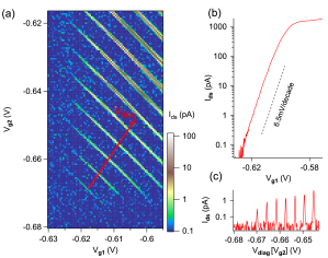
The metallic island is by design capacitively coupled to the gates of both transistors, hence at low temperature the drain-source current versus gate voltages and is a series of antidiagonal lines, as illustrated in Fig. 2a at 0.5 K. Each segment corresponds to the addition of an extra electron on the central island and is limited by the closure of the two FETs. In order to estimate the efficiency of each barrier separately we set one of them to +0.8 V to minimize its contribution to the total current and sweep the other one. Such a measurement is shown in Fig. 2b. As expected for industrial FETs, we found a very steep current rise over more than 4 orders of magnitude. At low temperature the sub-threshold slope is no more set by the ideal thermal activation discussed before but saturates, mainly because the conduction band is broadened by disorder. Despite this, the recorded value of 6.5 mV/decade at 0.5 K is excellent and critical for electron pumping. Fig. 2c shows the periodicity of the current recorded when both gates are varied in order to follow the red diagonal line drawn on top of Fig. 2a. The values =19.1 aF and =20.1 aF extracted from this graph illustrate the symmetry of the coupling to both FET gates.
III ELECTRON PUMPING
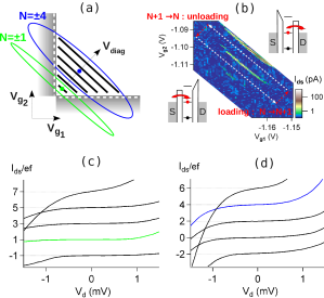
The principle of the pumping experiment is depicted in Fig. 3a,b. The white dashed line in Fig. 3a corresponds to the region where dc current measurement falls below the experimental noise floor because the barriers increase rapidly. Applying phase-shifted sinewaves on the gates corresponds to elliptic contours in the plane. They can be set to turn around a Coulomb peak without ever crossing a black segment where current flows. For this their center (set by the d.c. values of and ) has to be chosen on or near the Coulomb segment and the extension has to be large enough, as shown by the ellipses in Fig. 3a. This contour has been used previously with silicon but with extremely opaque barriers (always larger than ), resulting in extremely slow (1 MHz) and single-charge pumpingOno2003 . With barriers more than 6 orders of magnitude more transparent, we can pump faster and extend the contour to turn around several Coulomb lines, as illustrated by the blue ellipse in Fig. 3a. Instead of a net current for the green ellipse, one expects where is the number of Coulomb lines enclosed by the contour (=4 for the blue ellipse). The sign of the current is simply changed by turning in the other direction. Although never reported so far, the periodicity of the Coulomb oscillations should yield a different evolution of depending on the position of the contour center. With ellipses centered near a line, only odd numbers of lines are enclosed, while only even numbers occur for ellipses right in between two lines. These two situations have been experimentally realized. The corresponding pumped current plateaus are shown respectively in Figs. 3c,d. They follow exactly the expected odd/even behaviour.
The evolution of the slope of the plateaus as a function of different parameters have been investigated at high frequency. Results for sample s2 are shown in Fig. 4. The evolution of the pumped current versus is shown in Fig. 4a at 0.5 K, for =0. The rms amplitudes of the r.f. signals at 650 MHz on the gates are 19 mV and 19.8 mV, in order to account for the small difference in couplings to the two gates, and therefore align the long axis of the ellipse with the Coulomb segments pattern. The phase difference between the a.c. gate voltages was set 189∘, in order to pump preferentialy -1 electron. When the ellipse encloses only one Coulomb segment, a quantized plateau at /=-1 is obtained. Moving along , there are regions where two segments are partially enclosed. In that case there is a tendency to pump more than one electron, hence the recorded current periodically increases. This period (approximately 4.1 mV) is equal to the one extracted from the conductance measurements from which the gate capacitances given in Table 1 were obtained. A working point indicated by the cross in Fig. 4a is chosen to study the dependence of the pumped current with bias (Fig. 4b) and r.f. amplitude (Fig. 4c) and phase (Fig. 4d). An important figure of merit for a current source is its output resistance, corresponding to the flatness of the plateau in Fig. 4b. From the uncertainty in a linear fit of the data across a large span of (1.2 mV), in red, we obtain the lower limit of 250 G for this resistance. The flatness of the plateaus versus r.f. amplitude and relative phase are important to check that the flat region is wide enough to be well within control. The data shown in Fig. 4c,d gives a comfortable working range of 70 mV and 6∘.
Operation up to 1 GHz and for several values of is shown in Fig. 4e at 0.6 K. At =0 a plateau is still obtained up to , corresponding to a quantized current 1.12 nA. For this measurement with large , i.e. a wide ellipse, the r.f. amplitude has to be increased significantly to maintain a large penetration into the regions shaded in grey in Fig. 3a, where the island population will eventually change. A maximum rms amplitude of 33.5 mV was used (for =7 at =1 GHz), which is possible at 600 mK but could be challenging at significantly lower temperatures, where heating can occurChan2011 . It is clear however that the flatness quickly degrades with increasing , as a result of the inadequate trajectory looking too much like a circle. For better performance a custom trajectory performed with an arbitrary waveform generator could be used Giblin2012 .
While is determined near =0 by the number of Coulomb lines enclosed by the ellipse, it can be changed with a sufficient bias. This corresponds to the Coulomb staircase. In principle this is the case in any dot, however the barriers are often strongly affected by the bias and only the first diamond can be observed. In our system clear plateaus are still found up to 8 mV, with a period of approximately 4 mV (Fig. 4e) which can be directly interpreted as the charging energy (4 meV), without any lever-arm parameter. This is in excellent agreement with Coulomb diamond measurements (not shown). This behaviour in is characteristic of systems relying on orthodox Coulomb blockade, whether based on GaAsKouwenhoven1991 , SiChan2011 or a metal like here. It is strikingly different from the pumping scheme where the barriers are made more transparent than the quantum of conductance. In that case the middle island is fully connected to source or drain (hence there is no Coulomb blockade) and no dependence is found, even up to 200 mVFujiwara2004 . The possibility to observe clear plateaus with a bias voltage up to twice the charging energy is directly related to the robustness of the barriers in the OFF state, a figure of merit called drain-induced barrier lowering in microelectronics.
IV STABILITY AND ACCURACY EXPERIMENTS
The accuracy of the pumped current has been assessed with alternating current techniques, in order to cancel the offset of the measurement chain.
Firstly, preliminary current measurements using a cryogenic current comparator (CCC) have been carried out on a fourth sample, at a reduced frequency of 50 MHz with the CCC in internal feedback mode. Although this scheme does not allow an accurate measurement of the absolute value of the current, it allows to investigate the current steps flatness and the long-term stability of the device, shown in the supplementary material Steck2008 . The Allan deviation calculated for a 14-hour long measurement exhibits a variation with the averaging time . This is a signature of a white noise regime over the whole range of measurement time, up to 14 hours (Figures 1 and 2 of the supplementary material). The statistical uncertainty can therefore be estimated by calculating the experimental deviation of the mean over the whole set of data. It results in a relative statistical uncertainty of 3 parts in 106 on the current value.
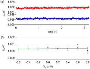
Secondly, calibrated commercial equipments have been used. Fig. 5a shows the time evolution of the currents obtained by switching the phase alternatively between 171∘ and 189∘, at 0.5 K, 650 MHz and =0. After changing the phase and waiting for 5 seconds, two points were recorded for each phase, with a 1 s integration time.
In order to evaluate the robustness of the obtained value with bias voltage, this alternating technique is used but on the much shorter timescale of a few tens of minutes, for which averaging out two-by-two subsequent values for + and - is beneficial (see supplementary material). Then this whole set of data points is averaged to yield a unique value for a certain . This final dataset is shown in Fig. 5b. The standard deviation of a linear fit (in green in Fig. 5b) across the 1.4 mV of gives a lower limit of 6.8 for the resistance. Averaging these 7 values yields a final current /=1.00036 across a 1.4 mV voltage bias span, at 650 MHz and 0.5 K, with a standard deviation of 0.00017. This value is well within the 0.15% uncertainty in the gain of our measurement setup after calibration.
V CONCLUDING REMARKS
The first experiments presented here on an industrial CMOS electron pump have been performed mostly at 650 MHz, in order to produce a pumped current of the order of 100 pA, high enough to be relevant for the quantum metrological triangle experiment. It should be noted that the experiments were carried out without any radiation shielding around the sample inside the vacuum chamber of a dilution refrigerator. Although our best value falls well below the accuracy of the measurement system, this could significantly improve further measurements with a more refined setup. The temperature of 0.5 K at which we did these experiments illustrates the small dimensions (high charging energy) of the nanowire transistors. However, a study in temperature will be needed now, in order to investigate the main cause of errors in the pumping mechanism. An important contribution to these errors may indeed come from the thermal broadening of the Coulomb lines. Another source of errors will arise from the finite steepness of the FETs sub-threshold slope. Clearly, when the working point is at an extremum of the ellipse, what matters is the ratio of the minimum resistance of one barrier and the maximum resistance reached by the other one Ono2003 . For bound to be larger than for Coulomb blockade operation, a resistance of has to be reached for the other one if one targets a relative uncertainty of . This kind of performance is probably reachable at low temperature with the FDSOI technology which shows unrivaled performance in terms of leakage. A more quantitative study is necessary, using the simulation tools we have developed for our Coulomb blockade devices and single-charge impurities Pierre2009 . A realistic simulation of the electrostatic system and tunable FET barriers has been implemented recently and will be compared with the experimental dataThe reproducibility and robustness of the fabrication technology ensures a consistent quality allowing very exhaustive experimental investigations, since these embedded samples do not age significantly. We have measured the same SET device based on SOI technology 6 years apart, and it has shown no significant modification in the pattern of Coulomb oscillations at low temperature. Another advantage of the nanowire transistors is that these pumps operate as FETs at 300 K. The room temperature measurements provide valuable information on the samples (e.g. maximum conductance, symmetry of the barriers) which allows to sort and select samples for low temperature investigation among the thousands available. A practical current standard based on this device can in addition benefit from straightforward integration with silicon technology. This includes on-chip CMOS circuits or drive electronics as well as r.f. design for 1-10 GHz operation. The authors acknowledge financial support from the French ANR under Project POESI, the EC FP7 FET-proactive NanoICT under Project AFSiD and the EMRP program under Project SIB-07 Quantum Ampere. The Nanosciences foundation is supporting this work with the PhD grant of P.C. We also thank Mark W Keller for his comments and careful reading of the manuscript.
References
- (1) J. Flowers, “The route to atomic and quantum standards,” Science 306, 1324 (2004)
- (2) B. N. Taylor and T. J. Witt, “New international electrical reference standards based on the josephson and quantum hall effects,” Metrologia 26, 47 (1989)
- (3) F. Piquemal and G. Genevès, “Argument for a direct realization of the quantum metrological triangle,” Metrologia 37, 207 (2000)
- (4) M. W. Keller, “Current status of the quantum metrology triangle,” Metrologia 45, 102 (2008)
- (5) H. Grabert and M. H. Devoret, Single Charge Tunneling: Coulomb Blockade Phenomena in Nanostructures (Plenum Press, New York, 1992)
- (6) L. J. Geerligs, V. F. Anderegg, P. A. M. Holweg, J. E. Mooij, H. Pothier, D. Esteve, C. Urbina, and M. H. Devoret, “Frequency-locked turnstile device for single electrons,” Phys. Rev. Lett. 64, 2691 (1990)
- (7) H. Pothier, P. Lafarge, C. Urbina, D. Esteve, and M. H. Devoret, “Single-electron pump based on charging effects,” EPL (Europhysics Letters) 17, 249 (1992)
- (8) L. P. Kouwenhoven, A. T. Johnson, N. C. van der Vaart, C. J. P. M. Harmans, and C. T. Foxon, “Quantized current in a quantum-dot turnstile using oscillating tunnel barriers,” Phys. Rev. Lett. 67, 1626 (1991)
- (9) M. W. Keller, J. M. Martinis, N. M. Zimmerman, and A. H. Steinbach, “Accuracy of electron counting using a 7-junction electron pump,” Appl. Phys. Lett. 69, 1804 (1996)
- (10) M. W. Keller, A. L. Eichenberger, J. M. Martinis, and N. M. Zimmerman, “A capacitance standard based on counting electrons,” Science 285, 1706 (1999)
- (11) S. V. Lotkhov, S. A. Bogoslovsky, A. B. Zorin, and J. Niemeyer, “Operation of a three-junction single-electron pump with on-chip resistors,” Appl. Phys. Lett. 78, 946 (2001)
- (12) X. Jehl, M. W. Keller, R. L. Kautz, J. Aumentado, and J. M. Martinis, “Counting errors in a voltage-biased electron pump,” Phys. Rev. B 67, 165331 ( 2003)
- (13) M. Pierre, B. Roche, X. Jehl, R. Wacquez, M. Sanquer, M. Vinet, N. Feltin, and L. Devoille, “Operation of a Silicon CMOS Electron Pump,” p. 755, 2010 Conference on Precision Electromagnetic Measurements, Daejeon, South Korea, June 13-18, 2010
- (14) J. P. Pekola, J. J. Vartiainen, M. Mottonen, O-P Saira, M. Meschke, and D. V. Averin, “Hybrid single-electron transistor as a source of quantized electric current,” Nat. Phys. 4, 120–124 ( 2008)
- (15) V. Maisi, Y. A. Pashkin, S. Kafanov, J.-S. Tsai, and J. Pekola, “Parallel pumping of electrons,” New Journal of Physics 11, 113057 (2009)
- (16) L. Nevou, V. Liverini, P. Friedli, F. Castellano, A. Bismuto, H. Sigg, F. Gramm, E. Muller, and J. Faist, “Current quantization in an optically driven electron pump based on self-assembled quantum dots,” Nat. Phys. 7, 423 ( 2011)
- (17) M. D. Blumenthal, B. Kaestner, L. Li, S. Giblin, T. J. B. M. Janssen, M. Pepper, D. Anderson, G. Jones, and D. A. Ritchie, “Gigahertz quantized charge pumping,” Nat. Phys. 3, 343 ( 2007)
- (18) A. Fujiwara, K. Nishiguchi, and Y. Ono, “Nanoampere charge pump by single-electron ratchet using silicon nanowire metal-oxide-semiconductor field-effect transistor,” Appl. Phys. Lett. 92, 042102 (2008)
- (19) B. Kaestner, V. Kashcheyevs, S. Amakawa, M. D. Blumenthal, L. Li, T. J. B. M. Janssen, G. Hein, K. Pierz, T. Weimann, U. Siegner, and H. W. Schumacher, “Single-parameter nonadiabatic quantized charge pumping,” Phys. Rev. B 77, 153301 (2008)
- (20) S. P. Giblin, S. J. Wright, J. D. Fletcher, M. Kataoka, M. Pepper, T. J. B. M. Janssen, D. A. Ritchie, C. A. Nicoll, D. Anderson, and G. A. C. Jones, “An accurate high-speed single-electron quantum dot pump,” New Journal of Physics 12, 073013 (2010)
- (21) S.P. Giblin, M. Kataoka, J.D. Fletcher, P. See, T.J.B.M. Janssen, J.P. Griffiths, G.A.C. Jones, I. Farrer, and D.A. Ritchie, “Towards a quantum representation of the ampere using single electron pumps,” Nat. Commun. 3, 930 ( 2012)
- (22) V. Kashcheyevs and B. Kaestner, “Universal decay cascade model for dynamic quantum dot initialization,” Phys. Rev. Lett. 104, 186805 ( 2010)
- (23) L. Fricke, F. Hohls, N. Ubbelohde, B. Kaestner, V. Kashcheyevs, C. Leicht, P. Mirovsky, K. Pierz, H. W. Schumacher, and R. J. Haug, “Quantized current source with mesoscopic feedback,” Phys. Rev. B 83, 193306 ( 2011)
- (24) Y. Ono and Y. Takahashi, “Electron pump by a combined single-electron/field-effect- transistor structure,” Appl. Phys. Lett. 82, 1221–1223 (2003)
- (25) K. W. Chan, M. Möttönen, A. Kemppinen, N. S. Lai, K. Y. Tan, W. H. Lim, and A. S. Dzurak, “Single-electron shuttle based on a silicon quantum dot,” Appl. Phys. Lett. 98, 212103 (2011)
- (26) M. Hofheinz, X. Jehl, M. Sanquer, G. Molas, M. Vinet, and S. Deleonibus, “Simple and controlled single electron transistor based on doping modulation in silicon nanowires,” Appl. Phys. Lett. 89, 143504 (2006)
- (27) B. Roche, B. Voisin, X. Jehl, R. Wacquez, M. Sanquer, M. Vinet, V. Deshpande, and B. Previtali, “A tunable, dual mode field-effect or single electron transistor,” Appl. Phys. Lett. 100, 032107 (2012)
- (28) A. Fujiwara, N. Zimmerman, Y. Ono, and Y. Takahashi, “Current quantization due to single-electron transfer in si-wire charge-coupled devices,” Appl. Phys. Lett. 84, 1323 (2004)
- (29) B. Steck, A. Gonzalez-Cano, N. Feltin, L. Devoille, F. Piquemal, S. Lotkhov, and A. B. Zorin, “Characterization and metrological investigation of an r-pump with driving frequencies up to 100 mhz,” Metrologia 45, 482 (2008)
- (30) M. Pierre, M. Hofheinz, X. Jehl, M. Sanquer, G. Molas, M. Vinet, and S. Deleonibus, “Background charges and quantum effects in quantum dots transport spectroscopy,” European Physical Journal B 70, 475 ( 2009)