Band structure and optical transitions in atomic layers of hexagonal gallium chalcogenides
Abstract
We report density-functional-theory calculations of the electronic band structures and optical absorption spectra of two-dimensional crystals of Ga2X2 (X=S, Se, and Te). Our calculations show that all three two-dimensional materials are dynamically stable indirect-band-gap semiconductors with a Mexican-hat dispersion of holes near the top of the valence band. We predict the existence of Lifshitz transitions—changes in the Fermi-surface topology of hole-doped Ga2X2—at hole concentrations cm-2, cm-2, and cm-2.
pacs:
73.61.Ga, 78.66.Hf, 73.20.-r, 71.15.MbI Introduction
Two-dimensional semiconductors have been studied intensively in the past few decades as researchers have tried to find materials to complement or even replace silicon in electronics. A recent trend in the hunt for new two-dimensional systems consists of the isolation and study of atomically thin sheets of layered materials. Honeycomb carbon allotropes have been widely investigated for this purpose following the discovery of graphene novoselov_2004 ; geim_2007 ; hexagonal boron nitride is another example BN01 ; BN02 . With increasing chemical unit cell complexity, hexagonal transition metal dichalcogenides have been exfoliated into atomically thin films using mechanical transfer and liquid-phase sonication mos2exfol ; KisA_2011_2 ; KisA_2011 ; WS2exp01 ; WS2exp02 ; many of these materials are semiconductors in both bulk and monolayer phases, making them ideal for use in single-sheet nanoscale optoelectronics KisA_2011_2 ; AtacaC_2012 ; WS2exp01 ; Morpurgo . In this work we explore the next generation in the family of two-dimensional atomic crystals: stoichiometric layers of gallium chalcogenides (Ga2X2).
In the bulk form, GaS and GaSe are indirect-gap semiconductors ho_ch_2006 , with the latter being well-known for its nonlinear optical properties bhar_gc_1995 , while GaTe is a direct-gap semiconductor used for electrothermal threshold switching Milne_WI_1973 . All three materials exhibit the same structure: they are layered compounds of Ga2X2 stoichiometry in which each layer consists of two AA-stacked hexagonal sublayers of gallium atoms sandwiched between two hexagonal sublayers of chalcogen atoms (X), as illustrated in Fig. 1. In a bulk material, these layers are bound in a three-dimensional structure by van der Waals interactions.
In this work we discuss the optical and electronic properties of single-layer crystals of Ga2S2, Ga2Se2, and Ga2Te2. We present the electronic band structures and optical absorption spectra for all three materials. In each case we find that the band gap is indirect, with the valence-band maximum shifted from the point (an inverted Mexican-hat dispersion) and the conduction-band minimum (CBM) located at the M point in Ga2S2 and Ga2Te2, and at the point in Ga2Se2. For all three materials we find an unusual, slightly anisotropic Mexican-hat shape in the electron dispersion near the edge of the valence band. However, the strongest peak in the optical absorption spectra—dominated by a transition between two bands with states which are even with respect to symmetry—is not caused by the Van Hove singularity associated with the Mexican-hat spectra, but is provided by two, near-parallel branches in the dispersion of the conduction bands near the Brillouin-zone corners K and K′. We also find that hole-doped Ga2X2 undergoes a Lifshitz transitionLifshitz1960 —a change in the topology of the Fermi surface—at hole concentrations cm-2, cm-2, and cm-2.

II Results and discussion
The band-structure analysis of single-layer Ga2X2 leading to the above conclusions was performed using density-functional-theory (DFT) as implemented in the castep castep and vasp vasp plane-wave-basis codes. Tests have shown that the two codes yield nearly indistinguishable results for the materials studied here. To calculate the geometries, phonon dispersions, and optical absorption spectra, we used semilocal exchange-correlation functionals: the local density approximation (LDA) and the Perdew-Burke-Ernzerhof pbe (PBE) functionals. The screened Heyd-Scuseria-Ernzerhof 06 (HSE06) functional hse was used to obtain the electronic band structures to compensate at least partially for the underestimation of the band gap by semilocal functionals. The plane-wave cutoff energy was 600 eV. During relaxations a Monkhorst-Pack k-point grid was used, while band structures were obtained with a grid. The optical absorption spectra were obtained with a very dense grid of k-points. The artificial out-of-plane periodicity of the monolayer was set to 20 Å. Phonon dispersions were calculated in castep castep2 using the method of finite displacements in a supercell, with k-points, a 408 eV plane-wave cutoff, and an artificial out-of-plane periodicity of 15.88 Å.
Full geometry optimization was performed using both the LDA and PBE functionals. Table 1 shows that the lattice constants increase with the atomic number of the chalcogen atom, while the Ga-Ga bond lengths hardly change. The bond lengths obtained with the PBE functional are systematically larger than those optimized with the LDA, as expected FavotF_1999 .
| X | ||||||
|---|---|---|---|---|---|---|
| S | ||||||
| Se | ||||||
| Te |
| X | |||
|---|---|---|---|
| S | eV | meV | meV |
| Se | eV | meV | meV |
| Te | eV | meV | meV |
| X | Kc | M | M | |
|---|---|---|---|---|
| S | ||||
| Se | ||||
| Te |
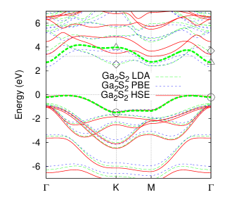
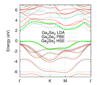
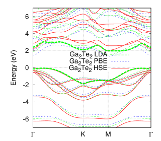
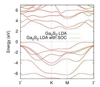
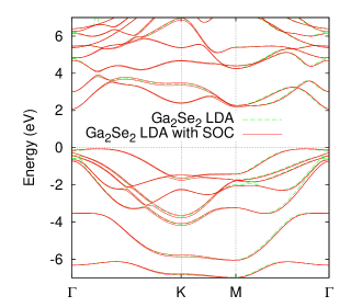
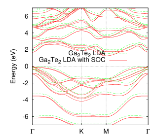
The calculated electronic band structures are summarized in Fig. 2. All three materials are indirect-gap semiconductors, primarily due to the valence-band maximum (VBM) lying somewhat off the point. It is possible to fit an inverted Mexican-hat polynomial to the valence-band dispersions around the valence band maximum:
| (1) |
where and are the polar coordinates of the wave vectors measured from the point in units of 1/Å, is measured from the line, and the energy is in units of eV. The coefficients are listed in Table 5. This fit should provide a good starting point for a simple analytical model of the valence band in these materials. Note however that this fit is designed to describe the immediate vicinity of the VBM and the saddle point, and it no longer describes the point correctly, overestimating the point valence band energy by 52 meV, 70 meV, and 32 meV in Ga2S2, Ga2Se2, and Ga2Te2, respectively.
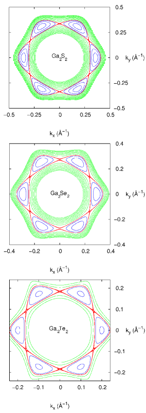
Further analysis of the valence band reveals a saddle point along the line, illustrated in Fig. 3. This saddle point gives rise to a Van Hove singularity in the density of states quite close to the Fermi level, which is found to be at the valence band edge. Due to the presence of these saddle points, hole-doping causes Ga2X2 to undergo a Lifshitz transition when the hole concentration reaches the critical value where all states are depleted above the energy of the saddle point, since this leads to a change in the topology of the Fermi surface. The carrier density where the Lifshitz transition takes place in each material is listed in the last column of Table 5 and was obtained by integrating the DFT density of states from the saddle point to the valence band edge.
We find that the conduction-band minimum (CBM) is at the M point in Ga2S2 and Ga2Te2, and at the point in Ga2Se2. The HSE06 band gaps of Ga2X2 are summarized in Table 2. The HSE06 band gap is expected to underestimate the quasiparticle band gap by no more than 10 % hse10percent , and is known to be applicable to two-dimensional materials as well hse10scuseria . Our finding that the gap is indirect is in agreement with a recent DFT result obtained for single-layer Ga2Se2 rybkovskiy_dv_2006 , although density-functional tight-binding calculations kohler_t_2004 disagree with our results for Ga2S2. The effective masses at the high-symmetry points in the conduction band are summarized in Table 3. The effective mass is isotropic at and K, but not at the M point.
The semilocal band structures are also plotted in Fig. 2 for comparison. The LDA and PBE functionals give very similar results to the HSE06 functional up to the Fermi level, but above that significant discrepancies arise. This is most notable in the case of Ga2S2, where the position of the CBM is ambiguous: the LDA predicts that the CBM is at the M point, in agreement with HSE06, while the PBE functional puts it at the point. In Ga2Se2 and Ga2Te2 both the LDA and the PBE functionals predict that the CBM is at the same place as in the HSE06 calculation.
In the case of the semilocal DFT calculations we also took spin-orbit coupling into account using a relativistic DFT approach vasp . As can be seen in Fig. 4 some of the bands exhibit spin splitting, including the highest valence () and lowest conduction () bands near the K point, most significant in Ga2Te2 (see Table 2). While we were unable to calculate the spin-orbit splittings in HSE06 due to limited computational resources, we expect that they will exhibit a similar magnitude to that found in the semilocal band structures.
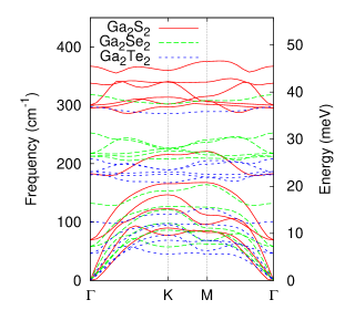
We have calculated the phonon dispersions for Ga2X2 using the force-constant approach in up to supercells. The results are depicted in Fig. 5, suggesting that isolated atomic crystals of gallium chalcogenides, Ga2X2, are dynamically stable.
Table 4 shows an orbital composition analysis of the LDA bands of Ga2S2 around the Fermi level. We have found that these bands are dominated by - and -type orbitals. Furthermore, states in each band are either odd or even with respect to symmetry (this information is obtained from the complex phases of the orbital decomposition in vasp). Therefore, the interband absorption selection rules require that photons polarized in the plane of the two-dimensional crystal are absorbed by transitions between bands with the same symmetry of wave-functions (eveneven, oddodd), and photons polarized along the axis cause transitions between bands with opposite symmetry (evenodd, oddeven). Note that in the case of Ga2Te2 these numbers only provide a qualitative description of whether the orbitals are of mostly or character due to the strong spin-orbit coupling.
| Band | K | ||
|---|---|---|---|
| 0.014+0.058+0.004+0.189 | 0.058+0.169+0.044 | ||
| 0.142+0.008+0.098+0.056 | 0.190+0.008+0.051 | ||
| 0.075+0.107+0.082+0.001 | 0.030+0.036 |
| X | E0 | E2 | E4 | E6 | E | |
|---|---|---|---|---|---|---|
| S | 1.38 | 5.6 | 1.634 | |||
| Se | 1.49 | 17 | 4.49 | |||
| Te | 2.50 | 240 | 30.1 |
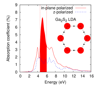
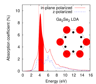
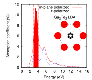
The calculated optical absorption spectra (using semilocal DFT) are shown in Fig. 6. The intensities were normalized by using graphene as a benchmark. We calculated the absorption of graphene using the same method in the 0.8–1.5 eV energy range where monolayer graphene absorbs 2.3 % of light, and used the calculated graphene absorption intensity to obtain a scaling factor that scales the calculated intensities to the experimental value. Since in the case of Ga2S2 we found disagreement between the PBE and the HSE06 regarding the location of the CBM, we restrict ourselves to the LDA in the following. Note that the LDA results are only qualitatively accurate and should only be used for a comparative study of the different Ga2X2 monolayers and for an order-of-magnitude estimate of the expected peak positions. A better description would require a computationally much more expensive calculation using the GW approximation and the Bethe-Salpeter equation for excitonic corrections bse_example . In Fig. 6 we show the energy dependence of the absorption coefficients of various stoichiometric Ga2X2 monolayers. The absorption spectrum starts with a shoulder at low energies, which originates from the vicinity of the M and points. In all cases the in-plane absorption is much more significant and is dominated by peaks at around 5 eV/4 eV/3.5 eV for X=S/Se/Te. Analysis of the band structure reveals that the bulk of this spectrum comes from transitions between the valence band and the even band above the conduction band around the K point where the two bands are near-parallel (this is the only part in the band structure where the energy difference between a filled and an empty band matches the energy of the main peak). In that range, the absorption coefficients of Ga2X2 are comparable to and even exceed that of monolayer and bilayer graphene; therefore we suggest that ultrathin films of GaX biased in vertical tunneling transistors with graphene electrodes could be used as an active element for detection of ultraviolet photons.
III Conclusion
We have shown using first-principles density-functional-theory that two-dimensional Ga2X2 (X=S, Se, and Te) crystals are stable indirect-band-gap semiconductors with an unusual inverted Mexican-hat valence band. The presence of saddle points along the line leads to a Lifshitz transition in the event of hole doping for which we have calculated the critical carrier density. We have provided an analytical fit of the valence-band edge and given a qualitative description of the optical absorption spectra, which suggest that ultrathin films of GaX biased in vertical tunneling transistors with graphene electrodes could be used as an active element for detection of ultraviolet photons.
Acknowledgements.
We acknowledge financial support from the EPSRC Science and Innovation Award, the ERC Advanced Grant “Graphene and Beyond,” the Royal Society Wolfson Merit Award, the Marie Curie project CARBOTRON, and the EC STREP “ConceptGraphene.”References
- (1) K. S. Novoselov, A. K. Geim, S. V. Morozov, D. Jiang, Y. Zhang, S. V. Dubonos, I. V. Grigorieva, and A. A. Firsov, Science 306, 666 (2004).
- (2) A. K. Geim and K. S. Novoselov, Nature Materials 6, 183 (2007).
- (3) Y. Kubota, K. Watanabe, O. Tsuda, and T. Taniguchi, Science 317, 932 (2007)
- (4) M. P. Levendorf, C.-J. Kim, L. Brown, P. Y. Huang, R. W. Havener, D. A. Muller, and J. Park, Nature 488, 627 (2012).
- (5) K. F. Mak, C. Lee, J. Hone, J. Shan, and T. F. Heinz, Phys. Rev. Lett. 105, 136805 (2010).
- (6) B. Radisavljevic, A. Radenovic, J. Brivio, V. Giacometti, and A. Kis, Nature Nanotechnology 6, 147 (2011)
- (7) B. Radisavljevic, M. B. Whitwick, and A. Kis, ACS Nano 5, 9934 (2011).
- (8) T. Georgiou, R. Jalil, B. D. Belle, L. Britnell, R. V. Gorbachev, S. V. Morozov, Y.-J. Kim, A. Gholinia, S. J. Haigh, O. Makarovsky, L. Eaves, L. A. Ponomarenko, A. K. Geim, K. S. Novoselov and A. Mishchenko, Nature Nanotechnology 8, 100 (2013).
- (9) J. N. Coleman, M. Lotya, A. O’Neill, S. D. Bergin, P. J. King, U. Khan, K. Young, A. Gaucher, S. De, R. J. Smith, I. V. Shvets, S. K. Arora, G. Stanton, H.-Y. Kim, K. Lee, G. T. Kim, G. S. Duesberg, T. Hallam, J. J. Boland, J. J. Wang, J. F. Donegan, J C. Grunlan, G. Moriarty, A. Shmeliov, R. J. Nicholls, J. M. Perkins, E. M. Grieveson, K. Theuwissen, D. W. McComb, P. D. Nellist, and V. Nicolosi, Science 331, 568 (2011).
- (10) D. Braga, L. I. Gutiérrez, H. Berger, and A. F. Morpurgo, Nano Lett. 12, 5218 (2012).
- (11) C. Ataca, H. Sahin, and S. Ciraci, J. Phys. Chem. C 116, 8983 (2012).
- (12) C. H. Ho and S. L. Lin, J. Appl. Phys. 100, 083508 (2006).
- (13) G. C. Bhar, S. Das, and K. L. Vodopyanov, Appl. Phys. B 61, 187 (1995).
- (14) W. I. Milne and J. C. Anderson, J. Phys. D.: Appl. Phys. 6, 2115 (1973).
- (15) I. M. Lifshitz, Sov. Phys. JETP 11, 1130 (1960).
- (16) S. J. Clark, M. D. Segall, C. J. Pickard, P. J. Hasnip, M. I. J. Probert, K. Refson, and M. C. Payne, Z. Kristallogr. 220, 567 (2005).
- (17) G. Kresse and J. Furthmüller, Phys. Rev. B 54, 11169 (1996).
- (18) J. P. Perdew, K. Burke, and M. Ernzerhof, Phys. Rev. Lett. 77, 3865 (1996).
- (19) J. Heyd, G. E. Scuseria, and M. Ernzerhof, J. Chem. Phys. 118, 8207 (2003); A. V. Krukau, O. A. Vydrov, A. F. Izmaylov, and G. E. Scuseria, ibid. 125, 224106 (2006).
- (20) K. Refson, P. R. Tulip, and S. J. Clark, Phys. Rev. B 73, 155114 (2006).
- (21) F. Favot and A. D. Corso, Phys. Rev. B 60, 11427 (1999).
- (22) S. Park, B. Lee, S. H. Jeon, and S. Han, Current Applied Physics 11, S337 (2011).
- (23) J. K. Ellis, M. J. Lucero, and G. E. Scuseria Appl. Phys. Lett. 99, 261908 (2011).
- (24) D. V. Rybkovskiy, I. V. Vorobyev, A. V. Osadchy, and E. D. Obraztsova, J. Nanoelectron. Optoelectron. 7, 65 (2012).
- (25) Th. Köhler, Th. Frauenheim, Z. Hajnal, and G. Seifert, Phys. Rev. B 69, 193403 (2004).
- (26) G. Onida, L. Reining, and A. Rubio, Rev. Mod. Phys. 74, 601–659 (2002).