Electronic transport in graphene Multilayers Electronic structure of graphene
Klein paradox for a pn junction in multilayer graphene
Abstract
Charge carriers in single and multilayered graphene systems behave as chiral particles due to the particular lattice symmetry of the crystal. We show that the interplay between the meta-material properties of graphene multilayers and the pseudospinorial properties of the charge carriers result in the occurrence of Klein and anti-Klein tunneling for rhombohedral stacked multilayers. We derive an algebraic formula predicting the angles at which these phenomena occur and support this with numerical calculations for systems up to four layers. We present a decomposition of an arbitrarily stacked multilayer into pseudospin doublets that have the same properties as rhombohedral systems with a lower number of layers.
pacs:
72.80.Vppacs:
73.21.Acpacs:
73.22.Pr1 Introduction
The electronic properties of the one atom thick graphene crystal has been the subject of several recent papers[1, 2] since its experimental isolation.[3] Not only is the crystal a promising candidate for semiconductor physics, the electron behavior also mimics that of Dirac particles and can therefore be seen as an interesting table top realization of a two dimensional quantum relativistic system. The Klein paradox, a unit transmission probability through potential barriers of any height or width, was one of the first characterizing phenomena from QED predicted[4] and subsequently observed experimentally[5]. But also optical properties as Fabry-Pérot resonances[6] and the negative refraction index that makes graphene a metamaterial[7] are remarkable properties of the crystal. The stacking of two layers of graphene, the so called bilayer graphene (BLG), although being only weakly bound, changes fundamentally the electronic properties. For example, the Klein paradox as observed in monolayer graphene (MLG) is replaced by the suppression of transmission which is called anti-Klein tunneling[8]. This suppressed transmission is remarkable since there are hole states available inside a potential barrier that are cloaked from the continuum of states outside[9]. For trilayer graphene (TLG), Klein tunneling is present if the layers are orthorhombic stacked. For Bernal stacking however Klein tunneling is absent[10, 11].
The occurrence of these tunneling phenomena is the consequence of the lattice induced chiral nature of the charge carriers. When the Fermi energy of the electrons is low enough, in MLG the dispersion of the electrons in the vicinity of one of the Dirac points K is linear in reciprocal space. This allows for the introduction of pseudospin, which is the lattice induced analogue of conventional spin from the Dirac theory. Extending this concept to BLG, the dispersion near the Dirac point can be approximated as being parabolic but due to symmetry arguments still leads to a spinorial Hamiltonian describing the electrons as chiral particles with a pseudospin[12, 13].
Some recent papers have discussed the electronic structure[14, 15] and known concepts such as trigonal warping and the Berry phase[16, 17, 18] of graphene multilayers. In this paper we generalize the discussions of Katsnelson et al.[4] and Gu et al.[9] to an arbitrary number of layers and to an arbitrary stacking order for a pn junction. We find that the low energy behaviour can be expressed as a system of non interacting pseudospin doublets, each with a specific chirality and derive a simple algebraic expression for the angles at which Klein tunneling (KT) and anti-Klein tunneling (AKT) can be expected.
2 Structure of the multilayer
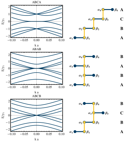
A system of layers of graphene can be stacked using a multitude of different stacking sequences. Graphene consists of two trigonal sublattices, called and , and it therefore suffices to consider only the relative position of these sublattices of the different layers. Due to the periodicity of the crystal, there are only three ways a layer can be placed with respect to the bottom one which we label as , and . It is possible to place it directly above the bottom layer (A), to shift it once (B) or twice (C) by the interatomic distance in the direction of the vector between the and atoms. Bernal stacking (ABA)[19, 20] is found to be the most stable combination. Rhombohedral stacking (ABC) is however also possible and is observed for a small number of layers[21, 22]. In between these two stacking structures, each different combination leads to a different electronic structure. To find the low energy electronic spectrum of the different possible stackings for an arbitrary number of layers, one can use the decomposition method as described by Min et al.[14]. Notice however that they do not differentiate between structures that are symmetric under in plane mirroring and thus represent the same system. The total number of physically different stacking possibilities for layers is given by
| (1) |
where refers to the nearest integer smaller than . The second term of this expression takes into account the mirror symmetry of a stacking sequence and is absent in the discussion of Ref.[14]. In Fig. 1 we show for the 3 stacking possibilities together with their respective energy spectrum near the point.
3 Rhombohedral multilayers
For rhombohedral (ABC) stacked graphene layers, the spectrum consists of two bands that touch at the point and bands that are located at higher energies. If we only include the nearest neighbour interlayer hopping, so only hopping between the and sublattices, the effective Hamiltonian of such system near the point is given by a matrix
| (2) |
with a vector of Pauli matrices, the Fermi velocity in MLG, the wave vector and is given by
| (3) |
where is the interlayer hopping parameter[23]. For this kind of stacking it is possible to introduce a two band low energy approximation which yields the Hamiltonian[14, 24]
| (6) | |||||
| (7) |
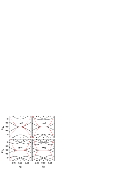
where is the angle of the wave vector with the normal chosen perpendicular to the pn junction and are the components of the pseudospin associated with this two dimensional Hamiltonian which are the respective Pauli matrices. The validity of this approximation is shown in Fig. 2 for . In this figure we show the dispersion relation obtained by the Hamiltonian in Eq. (2) which consists of bands. Superimposed we have plotted the dispersion relation from the Hamiltonian in Eq. (7) as dashed curves. The two band spectrum is in good agreement with the band spectrum for low energy and near the point.
The two band Hamiltonian in Eq. describes a chiral particle for which the pseudospin spins times as fast as the wave vector . Notice that for the angles
| (8) |
the sine or the cosine in Eq. vanish for even or odd respectively. At these angles the Hamiltonian commutes respectively with or making them conserved quantities.
When electrons impinge on a pn junction with an angle of incidence given by Eq. , conservation of pseudospin allows the electron to be reflected only if the reflected state has the same pseudospin as the incident state. The angle of the reflected state is given by and therefore the wave vector of the reflected electron must rotate by an angle of . Since the pseudospin rotates times as fast as the wave vector, we must have , , in order that reflection is allowed by pseudospin conservation. Using Eq. yields that the pseudospin of the reflected state is parallel with that of the incident state for angles when the difference is even, while the pseudospin is opposite when is odd.
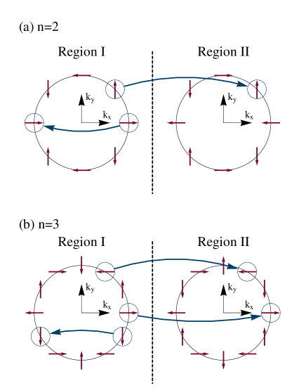
When the Fermi energy of the incident electron is less than the potential step of the pn junction, the sign of the wave vector of the propagating hole state inside the junction is opposite to the sign of the incident electron wave vector. This is the result of charge conservation at the steps’ edge and gives rise to a negative refraction index as found for MLG making it a meta-material[7, 6]. Due to the change in sign of the wave vector, the angle of the wave inside the potential region also flips sign, making the pseudospin inside the junction to rotate in the opposite direction. This is schematically illustrated in Fig. 3. In this case the angle of refraction is given by
| (9) |
where is the wave vector of the hole state and corresponds to the kinetic energy of the hole. Due to electron-hole symmetry, when , the refractive angle is exactly opposite to the angle of incidence. Following a similar argument as before, one finds that for angles the pseudospin is opposite to that of the incident state when is even, but it is the same when is odd.
A mismatch in the pseudospin inside and outside the potential step was invoked earlier to explain Klein tunneling in MLG and anti-Klein tunneling in BLG[4, 9]. Following the above argument, one can conclude that for an layered rhombohedral stacked system, AKT is present at angles given by Eq. when is even, while KT is present for angles given by Eq. when is odd. Table 1 lists the special angles for up to 5.
| n | (rad) | (rad) |
|---|---|---|
| 1 | ||
| 2 | ||
| 3 | ||
| 4 | ||
| 5 |
For arbitrary stacking, Min et al.[14] showed that the Hamiltonian can be decomposed in a set of independent pseudospin doublets of the form
| (10) |
where is the wave vector corresponding to the propagating low energy band of the pseudospin doublet and is the number of layers taking part in the doublet which corresponds to the chirality of this doublet. The number of pseudospin doublets depends on the details of the stacking, but the sum of the chiralities equals the total number of layers in the system. In this way one can decompose the low energy structure of any multilayered system in a set of non interacting doublets. Therefore, there are modes of propagation for low energy. As long as the symmetry of the system remains intact, it is not possible to scatter between different modes. The Hamiltonian given in Eq. is that of a system of rhombohedral stacked layers of graphene and because the different modes do not interact, the occurrence of KT and AKT is the same as before for a multilayer with .
4 Transmission probability
The two band Hamiltonian in Eq. has a plane wave solution given by two propagating waves, one right and one left moving, and evanescent waves. The wave vectors of these plane waves are the solutions of the equation
| (11) |
where and is the transverse wave vector. The solution of this equation is with different values for . The plane wave solution can be written as a two spinor
| (14) | ||||
| (15) |
where the latter is a matrix formulation of the spinor with matrices
| (16e) | ||||
| (16f) | ||||
| and | ||||
| (16g) | ||||
To find the transmission probability for a pn junction, one has to equate the plane wave solutions and all the derivatives up to order of the region before the junction (region I) with those of the region behind it (region II) at the junction’s edge at . This leads to a set of two component equations:
| (17) |
where the matrix is evaluated at . Normalizing the incident wave on the right propagating wave before the junction by putting and applying boundary conditions and for to suppress the non normalizable plane wave functions, the transmission and the reflection probability are given by
| (18) |
The numerical results for the transmission probability for multilayers with up to are depicted in Fig. 4 as function of the energy of the incident electron and the incident angle. The expected angles for KT and AKT are confirmed by our calculations.
Fig4.eps
5 Conclusions and remarks
The combination of the chiral nature of the charge carriers and their meta-material properties induce Klein tunneling and anti-Klein tunneling at specific angles for rhombohedral stacked graphene multilayers. For an arbitrary stacking sequence, the low energy behavior of the electrons can be decomposed in independent chiral doublets with a chirality that act as if it is a rhombohedral multilayer with layers. In this way, for any arbitrary stacking sequence, one can predict the occurrence of Klein tunneling and anti-Klein tunneling. Note however that we limited ourselves to nearest neighbour hoppings and neglected other less important hoppings that are present in a real multilayer. The latter results in e.g. trigonal warping[18] that will effect our results for very small energies. Furthermore, the use of the two band approximation limits the energy range to about 300meV. At high energies, additional modes of propagation need to be taken into account, changing the transmission properties for high junctions and high Fermi energy[13].
Acknowledgements.
We thank S. Gillis for valuable discussions. This work was supported by the European Science Foundation (ESF) under the EUROCORES Program Euro-GRAPHENE within the project CONGRAN, and the Flemish Science Foundation (FWO-Vl).References
- [1] \NameCastro Neto A. H., Guinea F., Peres N. M. R., Novoselov K. S. Geim A. K. \REVIEWReviews of Modern Physics812009109.
- [2] \NameRozhkov A. V., Giavaras G., Bliokh Y. P., Freilikher V. Nori F. \REVIEWPhysics Reports503201177.
- [3] \NameNovoselov K. S., Geim A. K., Morozov S. V., Jiang D., Zhang Y., Dubonos S. V., Grigorieva I. V. Firsov A. A. \REVIEWScience3062004666.
- [4] \NameKatsnelson M. I., Novoselov K. S. Geim A. K. \REVIEWNature Physics22006620.
- [5] \NameStander N., Huard B. Goldhaber-Gordon D. \REVIEWPhysical Review Letters1022009026807.
- [6] \NameRamezani Masir M., Vasilopoulos P. Peeters F. M. \REVIEWPhysical Review B822010115417.
- [7] \NameCheianov V. V., Fal’ko V. Altshuler B. L. \REVIEWScience31520071252.
- [8] \NameCampos L.C., Young A.F., Surakitbovorn K., Watanabe K., Taniguchi T. Jarillo-Herrero P. \REVIEWNature communications320121239.
- [9] \NameGu N., Rudner M. Levitov L. \REVIEWPhysical Review Letters1072011156603.
- [10] \NameKumar S. B. Guo J. \REVIEWApplied Physics Letters1002012163102.
- [11] \NameVan Duppen B. Peeters F. M. \REVIEWApplied Physics Letters1012012226101.
- [12] \NameMcCann E. Falḱo V. \REVIEWPhysical Review Letters962006086805.
- [13] \NameVan Duppen B. Peeters F. M. \REVIEWPhysical Review B2012 Four band tunneling in bilayer graphene (Submitted).
-
[14]
\NameMin H. MacDonald A. H. \REVIEWPhysical Review B772008155416.
Please note that the - and the -tetralayer are considered to be different systems, while it is the same under mirror symmetry and the permutation . - [15] \NameKoshino M. McCann E. \REVIEWPhysical Review B872013045420.
- [16] \NameMorimoto T. Koshino M. \REVIEWPhysical Review B872013085424.
- [17] \NameMikitik G. P. Sharlai Yu. V. \REVIEWLow Temperature Physics342008794.
- [18] \NameKoshino M. McCann E. \REVIEWPhysical Review B802009165409.
- [19] \NameBernal J. D. \REVIEWProceedings of the Royal Society A: Mathematical, Physical and Engineering Sciences1061924749.
- [20] \NamePartoens B. Peeters F. M. \REVIEWPhysical Review B752007193402.
- [21] \NameShih C.-J., Vijayaraghavan A., Krishnan R., Sharma R., Han J.-H., Ham M.-H., Jin Z., Lin S., Paulus G. L., Reuel N. F., Wang Q. H., Blankschtein D. Strano M. S. \REVIEWNature Nanotechnology62011439.
- [22] \NameCraciun M. F., Russo S., Yamamoto M., Oostinga J. B., Morpurgo A. F. Tarucha S. \REVIEWNature Nanotechnology42009383.
- [23] \NamePartoens B. Peeters F. M \REVIEWPhysical Review B742006075404.
- [24] \NameNakamura M. Hirasawa L. \REVIEWPhysical Review B772008045429.