Ballistic charge transport in graphene and light propagation in periodic dielectric structures with metamaterials: a comparative study
Abstract
We explore the optical properties of periodic layered media containing left-handed metamaterials. This study is based on several analogies between the propagation of light in metamaterials and charge transport in graphene. We derive the conditions for these two problems become equivalent, i.e., the equations and the boundary conditions when the corresponding wave functions coincide. We show that the photonic band-gap structure of a periodic system built of alternating left- and right-handed dielectric slabs contains conical singularities similar to the Dirac points in the energy spectrum of charged quasiparticles in graphene. Such singularities in the zone structure of the infinite systems give rise to rather unusual properties of light transport in finite samples. In an insightful numerical experiment (the propagation of a Gaussian beam through a mixed stack of normal and meta-dielectrics) we simultaneously demonstrate four Dirac point-induced anomalies: (i) diffusion-like decay of the intensity at forbidden frequencies, (ii) focusing and defocussing of the beam, (iii) absence of the transverse shift of the beam, and (iv) a spatial analogue of the Zitterbewegung effect. All of these phenomena take place in media with non-zero average refractive index, and can be tuned by changing either the geometrical and electromagnetic parameters of the sample,or the frequency and the polarization of light.
I Introduction
Highly unusual properties of monolayers of graphite (graphene) and of optical media with negative refractive indices (left-handed metamaterials) had been independently predicted and studied theoretically a long time ago 1 ; 2 . At that time, however, these predictions were perceived as rather intriguing but unrealistic exotica, and remained unnoticed for about a half-century, until quite recently (and nearly simultaneously) they were embodied in real materials. This immediately triggered an explosion of interest and activities, in metamaterials and graphene, both in solid state physics and optics. Researchers also realized that the most unusual properties of electron transport in graphene were also peculiar to the propagation of light in dielectric systems with metamaterials. Mathematically, this is because, under some (rather general) conditions, the Maxwell equations for electromagnetic waves in an inhomogeneous dielectric medium can be reduced to the Dirac equations for charge carriers in graphene subjected to an external electric potential.
I.1 Similarities between Maxwell and Dirac equations
The history of recasting Maxwell equations in alternative, more compact, spinor forms goes back to the beginning of the past century, and is still in progress (for a comprehensive historical overview see Refs. 3, ; 4, , with recent examples in Refs. 5, ; 6, ; 7, ; 7a, ). Therefore it is not surprising that the similarity between Maxwell and Dirac equations has long been noticed (according to Ref. 3, , Majorana discussed it already in 1930). In the general case of inhomogeneous media, the close analogy between (i) the quantum-mechanical form of the equations for the Reimann-Silberstain vector fields (linear combinations of the electromagnetic vectors and ), and (ii) the Dirac equation, written in the chiral representation of the Dirac matrices, was explicitly demonstrated in Ref. 3,
Recently, as graphene became increasingly more popular in solid state physics, the mathematically established similarity of Maxwell and Dirac equations took on a new physical significance. Inspired by the very unusual predictions and discoveries made in graphene, research groups in optics started endeavors to reproduce the unique transport properties of graphene in specifically designed dielectric structures. An additional incentive to these efforts came from the fact that, while the elementary building blocks of graphene are fixed, modern micro- and nanotechnologies enable manufacturing periodic dielectric samples with a variety of types and sizes of unit cells. Moreover, the electrodynamic parameters of photonic crystals can, in principle, be controlled by external fields, providing unique opportunities to study condensed matter phenomena in optical ways; for example, by opening a gap between Dirac cones, as well as breaking and restoring space-inversion and time-reversal symmetries 5 . Rather simple electrodynamical analogies furnish physical insights into properties and applications of graphene such as: the Klein phenomenon Shytov , breaking the valley degeneracy Garcia , graphene quantum dots Darancet ; Rozhkov , the electronic Goos-Hanchen shift Chen , delocalization in one-dimensional disordered systems 8 , etc. Furthermore, some exotic phenomena predicted and discovered in optical systems (like, for example, the “light wheel” localized mode A , or confined cavity modes and mini-stop bands in broad periodic photonic waveguides B ; C ) could prompt unique possibilities for creating new graphene-based devices. In this regard, particularly promising is the analogy between photonic crystal broad waveguides and zigzag graphene nanoribbons studied in Ref. D, , where it was shown that the photonic mode coupling also arises in nanoribbons at low energies. The implementation of the analogy between Dirac electrons and light could be rewarding for the optical community as well, because it is relatively easy to create in graphene an inhomogeneous potential pattern with any distribution of and junctions, while designing a periodic or random stack of alternating positive-negative dielectric layers is nowadays a feasible task. Thus, graphene could provide analogue laboratory models in order to test the optics of metamaterials in a controlled way.
I.2 Dirac point
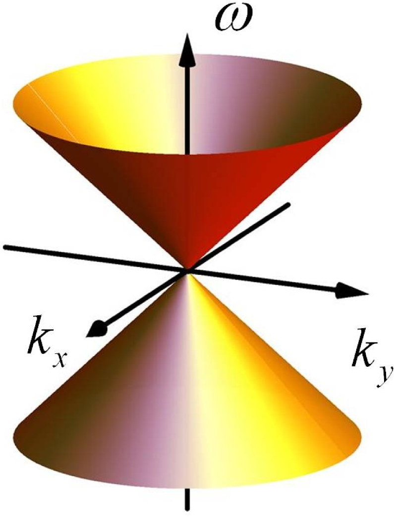
The key feature of graphene, from which all its unique transport properties stem, is the existence of Dirac cones in the band structure of its energy spectrum. At first glance, one does not have to work hard to obtain in optics a double-conical, graphene-like dispersion law: it is inherent in any plane monochromatic wave propagating in a homogeneous medium, as the relation between its frequency and the wave number is given by
| (1) |
However, the contact of two cones in Fig. 1 only looks like a Dirac point (DP). In fact, of the two cones in Fig. 1, only one (for example, the upper one) is related to a photon, while the second solution of Eq. (1) (lower cone in Fig. 1) is redundant. This lower cone does not carry any additional information and is not related to any different physical entity like, for example, a hole in graphene or a positron in the case of relativistic QED. In other words, the photon and antiphoton are identical 3 . Hence, the challenge in optics is to create a structure with a real DP in its spectrum, so that different types of waves would correspond to two different cones (a sort of optical “particle-antiparticle” pair). Appropriate for this purpose are photonic crystals, in which two modes degenerated in a homogeneous space become split by the periodicity 9 .
The analytical and numerical studies of two-dimensional periodic structures (infinite rods embedded in a background medium with a different dielectric constant) were carried out as early as in 1991, for square 10 and triangular 11 lattices. Linear singularities (that nowadays are called Dirac points) are clearly seen in the band structures of both systems, although they escaped the attention of Refs. 10, ; 11, mostly interested in absolute band gaps for different polarizations. Afterwards, during more than two decades, studies of two-dimensional photonic crystals were primarily aimed on maximizing the photonic band gap 12 ; 15 ; 16 (see also the review Ref. 17, and references therein), until the discovery of the unusual transport properties in graphene, and the potential to reproduce them in optics switched efforts towards the search and further exploration of photonic structures with Dirac-cone-like singularities in their transmission spectra 5 ; 7 ; 9 ; 18 . A number of new optical phenomena arising due to the existence of Dirac points were predicted and discovered: diffusion-like -dependence of the pulse intensity on the distance of propagation inside the photonic crystal 9 ; 19 (which is unusual for non-random media); oscillatory motion of a Gaussian beam (optical analogue of the Zitterbewegung effect) 20 ; 21 ; 22 ; extinction of coherent backscattering 23a ; 23b ; 23 ; conical diffraction 24 ; as well as the existence of graphene-like and novel edge states 25 ; 25a .
From the above-mentioned publications one can conclude that the existence of Dirac points in two-dimensional periodic structures is a rather universal phenomenon, in the sense that they appear irrespective of sample details, such as the shape and dielectric parameters of the “atoms” and its structural symmetry. For example, in the band structures presented in Refs. 7, ; 10, ; 11, ; 26, , DPs show up at square, triangular, and honeycomb lattices. The general criteria for the existence of DP in periodic dielectric samples were discussed in Ref. 27, .
The situation in layered periodic media is quite different and less studied. As we show below, DPs cannot exist in periodically-layered dielectric structures built of mono-type (i.e., with either all positive or negative refractive indices) dielectrics, no matter their period, size, and dielectric contrast between the layers. In Refs. 27, ; 34, , a one-dimensional periodic array of metallic unit cells of a special shape was considered, which exhibited Dirac points created by the accidental degeneracy of two modes. To create photonic Dirac cones in one dimension, both normal and metamaterials should be used. Interestingly enough, a single DP can exist in a homogeneous dispersive meta-medium at a frequency at which both the dielectric permittivity and the magnetic permeability approach zero simultaneously 6 . Eigenwaves in structured, infinite periodic systems built of alternating normal and left-handed dielectric layers, and the transmission and reflection from finite samples, were analyzed in Refs. 36, ; 37, ; 38, . It was shown that, when the spatial average of the refractive index over the period was zero, the band structure consisted of gaps at all frequencies except for a set of isolated points (discrete modes), for which the optical thicknesses of the adjacent layers were equal to the same integer number of half-wavelengths. New Dirac cones in graphene supelatices created by double-periodic and quasiperiodic electrostatic potentials have been considered in Ref. Japan, .
I.3 Brief summary
Here we study the transport properties of layered periodic dielectric systems “electronically similar” to graphene, in the sense that they possess Dirac cones in their photonic band gap structures. In Sec. II, we demonstrate, using a simple example, and discuss the similarity and differences between the Maxwell and Dirac equations as well as between the corresponding boundary conditions. Section III presents the transmission through potential barriers created in graphene by applying steplike electrostatic potentials, in comparison with light propagation in slabs of normal dielectrics and metamaterials. In Sec. IV, the photonic band-gap structures of periodically layered dielectrics are compared with the structure of the electron energy zones of graphene subjected to a periodic potential. It is shown that, unlike a two-dimensional photonic crystal, Dirac cones in a layered periodic medium can exist only when the medium consists of alternating slabs of left- and right-handed dielectrics (mixed samples). In Sec. V, we study the propagation of Gaussian beams of light through periodically-layered mixed samples built of alternating slabs with positive and negative refractive indices, and of beams of charge carriers through finite graphene superlattices. We demonstrate the anomalous, diffusion-like dependence of the intensity on the propagation distance, and an analog of the Zitterbewegung effect in a wide range of parameters. New unusual transport properties of such samples are predicted. In particular, it is shown that two contacting Dirac cones manifest themselves differently: given two beams with frequencies belonging to different cones, one is focused and another is defocused. The magnitude of the shift of the focus is independent on the distance of the sample from the focal plane of the incident beam and is proportional to the width of the sample. At oblique incidence, a Gaussian beam is not displaced along the sample even at non-zero values of the mean value of the dielectric constant.
II Equations and boundary conditions
The dynamics of the charge carriers in an external potential in graphene is described by a spinor
whose components are related to two sublattices in the unit cell of the crystal 39 . In the low-energy limit, near the Dirac point, the components of this spinor obey the Dirac equations. When the energy of the charge carrier is fixed, then the time dependence of the spinor is given by , and these equations can be written as
| (2) |
where is the electrostatic potential, and is the Fermi velocity.
In order to link this to Maxwell equations, we now consider, as an example, a TE electromagnetic wave (where the magnetic field has only one non-zero component) propagating in a homogeneous medium, and introduce two complex-valued functions
| (3) |
where is the medium impedance, and are the medium permeability and permittivity, accordingly. In Ref. 3, , instead of Eq. (3), the Reimann-Silberstain vector wave functions were used to derive a quantum-mechanical, matrix form of the classical wave equations in the general case of arbitrary electromagnetic fields propagating in media with space-dependent permittivity and permeability. The analogy with the relativistic Dirac equations was noted.
It is easy to show that for monochromatic fields and [the time dependence is given by ], the Maxwell equations yield
| (4) |
Here, is the medium refractive index, and . It is evident that after the replacement
| (5) |
Eq. (II) coincide with Eq. (II). Namely, the 2D Maxwell equations for the complex effective fields (3) in a homogeneous medium, and the Dirac equations for the wave functions of the charge carriers in graphene become identical. The role of the refractive index of the corresponding effective medium is played by the quantity . Therefore if, for example, the potential is a piecewise-constant function of one coordinate, the corresponding graphene superlattice models a layered dielectric structure 8 . In particular, a layer, in which the potential exceeds the energy of the particle, , is similar to a slab with negative refractive index . This means that a junction of two regions having opposite signs of is similar to an interface between left- and right-handed dielectric media with the refractive indices and , if
| (6) |
Because of this similarity, a junction can focus Dirac electrons in graphene 41 in the same way as the focusing of electromagnetic waves by the boundary between a normal dielectric and a metamaterial 1 ; 42 . However it is important to realize that, as it follows from Eq. (6), a change of necessarily implies the corresponding change of the ratio . Thus, to model the same (i.e., with fixed values of and ) graphene bi-layer structure, but at different energies, one has to chose different pairs of dielectrics.
It follows from Eq. (II) that the energy spectrum of the charge carriers in graphene in a homogeneous potential is linear near , i.e., consists of two cones touching at the Dirac point (see Fig. 1):
| (7) |
After substituting Eq. (II), Eq. (7) looks exactly like the dispersion law (1) for photons. Whilst Eqs. (2) and (4) are akin, the similarity between the two problems is not complete. First, unlike Dirac wavefunctions, the genuine electromagnetic fields and are real, i.e., equal to their complex conjugates. Due to this, positive and negative frequencies (upper and lower cones in Fig. 1) correspond to the same fields, in contrast to a Dirac spinor, which describes electrons, when , and holes, when . One further distinction is that the electric field satisfies the continuity condition
| (8) |
which is not required for the Dirac wave functions.
Essentially different are also the boundary conditions for the Dirac wave functions at the interface between two half-spaces with potentials and ,
| (9) |
and for the effective electromagnetic fields and at the boundary between two dielectrics:
| (10) |
Equations (10) follow from the boundary conditions for the real fields, and (the boundary is assumed to be parallel to the axis ).
Although the charge transport in graphene and the light propagation in dielectrics are governed by similar equations (II) and (II) inside the medium, the boundary conditions (9) and (10) are distinct from each other. This means that, generally speaking, the coupling between adjacent samples in these two cases is different. This difference is more conspicuous in the particular case of a monochromatic plane wave, , when the boundary conditions for the effective fields take the form:
| (11) |
where . It is easy to see that Eqs. (9) and (11) coincide only when (normal incidence) and . That is, in this particular instance, the transmission of Dirac electrons through a junction is similar to the transmission of light through an interface between two media with different refractive indices but equal impedances. In other words, at normal incidence, any junction in graphene, either , , or , is analogous to a contact between two perfectly-matched dielectrics or microwave elements. Such an interface is absolutely transparent to the normally-incident radiation and therefore to the Dirac electrons in graphene as well. This provides a more intuitive insight into the physics of the Klein paradox (perfect transmission through a high potential barrier 39 ; 43 ) in graphene systems.
III Transmission through potential barriers and dielectric slabs: similarities and differences
To compare the transport properties of Dirac electrons and light in the general case of oblique incidence, , we first consider the transmission of particles through a step-like potential barrier, i.e. through the line separating two domains (1 and 2) of a graphene sheet with different values and of the potential. In what follows, we will consider only one spinor component, say , because could be found using Eq. (II). The solutions of Eqs. (II) in both domains can be presented as a linear combination of plane waves with equal (at the chosen geometry of the system) values of :
| (12) |
From now on we consider the range of parameters where there are no total internal reflections and therefore . From the continuity of the wave functions at the boundary, Eq. (9), it follows (the incident wave now propagates from medium 1 to medium 2):
| (13) |
where the transfer matrix for the interface is equal to
| (14) |
and the matrix elements are
| (15) |
Here , and are the angles of incidence and refraction, respectively, while .
We determine the transmission and reflection coefficients as the ratios of the normal-to-the-boundary components of the densities of the transmitted, , and reflected, , currents divided by the normal component of the incident current density :
| (16) |
where
| (17) |
From Eqs. (16), (17) the following formulas can be obtained (see, e.g., Refs. Bliokh, ; Allian, ):
| (18) |
where the angles of incidence and refraction are connected by the relation
| (19) |
The same signs of and correspond to (or ) junctions, while for a (or ) junction . It is easy to see that at normal incidence () the potential barrier of any height is absolutely transparent at any energy (the Klein tunneling effect).
In the case of light propagating through the interface between two dielectrics, whose parameters are , and , , the transfer matrix
| (20) |
connects the amplitudes of leftward and rightward propagating waves at both sides, and has the same form as Eq. (14), with the matrix elements replaced by
| (21) |
for TE waves, and by
| (22) |
for TM radiation. In Eqs. (21) and (22), , , and . For left-handed dielectrics (, ), the refractive index is negative.
When , the expressions (21) and (22) are identical and are related to the matrix elements (15) of the corresponding transfer matrix in graphene, Eq. (13), as
| (23) |
This relation is a consequence of the abovementioned difference between the solutions of the Dirac and Maxwell equations: the former are complex-valued functions, while the electromagnetic fields are real.
The light transmission and reflection coefficients are determined as the ratios of the normal components of the transmitted (for ) and reflected (for ) energy fluxes divided by the normal component of the incident energy flux. When (the situation most favorable for the analogy between Dirac electrons and light) and take the forms:
| (24) |
One can see that even in the particular case, , Eqs. (III) and (III) are, generally speaking, different, and coincide only when , i.e., when the boundary conditions Eq. (11) are equivalent. This means that in spite of the identity of Eqs. (II) and (II), the analogy between the transport of Dirac electrons in graphene and electromagnetic radiation in dielectrics should not be extended too far. Due to the differences in the boundary conditions, the analogy holds only for normal incidence on the interface between two perfectly matched media.
The transmission of Dirac electrons trough a potential barrier of finite width , and of an electromagnetic wave through a dielectric slab of the same width are described by similar matrices of the form
| (25) |
where the indices 1 and 2 now correspond, respectively, to the outside and inside of the barrier (slab). The matrix is equal to , as in Eq. (14) for graphene, and , as in Eq. (20) for dielectrics. Obviously, , where is a unit matrix. The diagonal matrix , with describes the propagation inside the barrier (dielectric slab). From Eq. (25) it follows that under the condition
| (26) |
. This means that either a potential barrier or a layer of dielectric is transparent if its width is equal to an integer number of half-wavelengths. This is a general property of both, Dirac and Maxwell equations, which is independent of the ratio between the impedances, and its physical nature has nothing to do with the Klein tunneling.
IV Periodically-stripped graphene superlattices and photonic structures
In this section, we compare the structure of the electron energy zones of graphene subject to a periodic electrostatic potential, with the photonic band gap structures of periodically-layered dielectrics. To do this we assume that the potential in graphene takes the two values and in alternating areas of widths and , and the corresponding dielectric sample is built of alternating layers of the same thicknesses, and , with refractive indices and , and impedances and , respectively. In both cases, the propagation in the layers 1 and 2 is described by the matrices , , where . Assuming that the layers are parallel to the -axis, the transformation matrix on the period is defined by , and is equal to
| (27) |
for graphene, and
| (28) |
for dielectrics.
The eigenvalues ( is the Bloch wavenumber along the -axis) of the matrix () depend on the energy (frequency) and on the tangent component of the wavevector. Both periodic structures are transparent if
| (29) |
In other words, Eq. (29) determines the transparency zones: the ranges of the energies (frequencies) and wave numbers for which the longitudinal wavenumber is real 45 . It can be shown that
| (30) |
where
| (31) |
for Dirac electrons in graphene and
| (32) |
for electromagnetic waves in layered dielectrics. In both cases, the eigenmodes obey the dispersion equation:
| (33) |
It follows from Eqs. (29) and (30) that a periodic structure is transparent for the points in the plane [or ] for which the inequality holds. One the other hand, in each of these two planes, the conditions
| (34) |
( and are positive integer numbers) determine two sets of curves, where and are equal to . This means that those types of curves belong to transparency zones. It is apparent that since at the crossings of these lines, the eigenvalues of the matrices and are equal to , such singular crossing points lie at the edges of the zones and represent their points of contact, known as “conical intersection,” or “diabolic points” (see, e.g., Ref. Berry, ).
The coordinates, and , of these points in the plane can be found from Eqs. (IV):
| (35) |
In the case of graphene, the coordinates of the diabolic points in the plane are calculated in the same way. In the vicinity of the points defined by Eq. (IV), the phases and can be written as
| (36) |
where . Substituting Eqs. (36) into Eq. (32) yields:
| (37) |
with
where the components and are taken at the point . In the plane , where and are small deviations of and from their values given by Eq. (IV), the points for which the quadratic form (IV) is positive, constitute a transparency zone, while the points with correspond to a gap in the photonic spectrum.
The relation between , , and follows from the formula:
| (38) |
where is the refraction index of the -th layer. An analogue formula for graphene has the form:
| (39) |
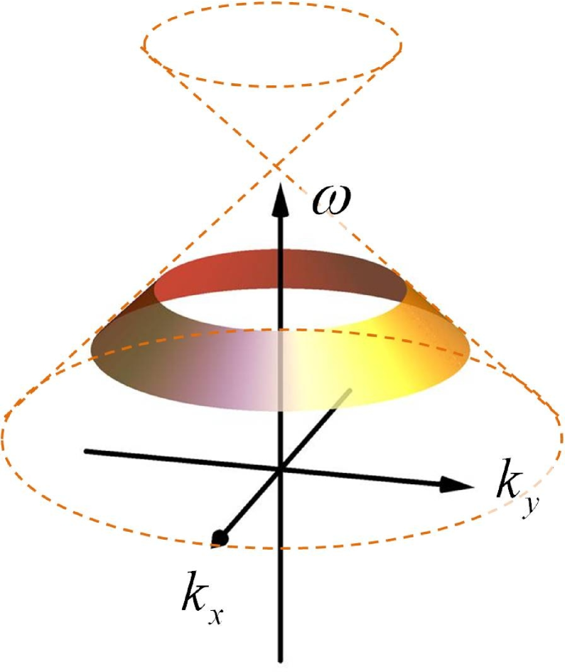
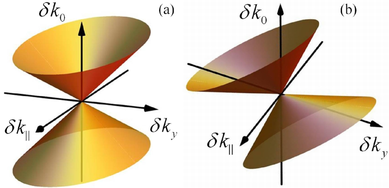
While in conventional dielectrics, the dispersion can be ignored, if it is weak enough, in left-handed materials it must always be taken into account. Indeed, the surface , where , for normal dielectrics, is a cone similar to the one presented in Fig. 1; i.e., , with . For left-handed metamaterials , and the group velocity is negative, , i.e., is antiparallel to the phase velocity . The surface , in a small vicinity of a certain frequency , has the form depicted in Fig. 2. Although locally it looks like a part of the lower cone in Fig. 1, , with on this surface, because the contact point of the cones is shifted from the origin.
Although the absolute values of the transmission and reflection coefficients in Eqs. (III) and (III) are different, the dispersion characteristics of two adjoining right- and left-handed dielectric layers, and the energetic spectrum diagrams of junction in graphene are identical, as it is shown schematically in Fig. 3. As a consequence of this identity, the periodic dielectric structure and graphene superlattice formed by a periodic external potential possess the same unique transport properties.
IV.1 Photonic structure
From Eq. (38) we obtain:
| (40) |
where is the wave group velocity in the -th layer at the frequency . The group velocity in Eq. (40) is positive for normal dielectric layers, and negative for layers of left-handed metamaterials.
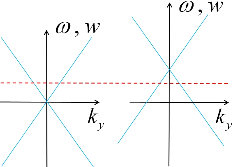
Equation (40) shows that the phase variations vanish on the lines
| (41) |
These lines lie in the transparency zones and intersect at the point where they touch. The line associated with the right-handed dielectric lies in the first and the third quadrants, whereas the line associated with the left-handed metamaterial lies in the second and the fourth quadrants, as it is shown in Fig. 4. When the lattice is composed of conventional dielectrics only, both lines and lie in the first and the third quadrants, and the transparency zones touch one another in a manner shown in Fig. 4(a). There are band gaps above and below the frequency , and these gaps are degenerate in pointlike nontransparent zones (gaps) at the frequency . Note that the zone structure of the lattice composed of both left-handed dielectrics is similar to the one shown in Fig. 4(a), but symmetrically reflected with respect to the axis.
The band structure can be significantly different when the lattice contains both left- and right-handed dielectrics. In this case, there are transparency zones above and below the frequency , that touch one another at the frequency , forming a pointlike transparent zone as it is shown in Fig. 4(b). This band structure is similar to the energy spectrum of the charge carriers in graphene, and manifests genuine Dirac points. It must be emphasized that for such points to exist, the layers with both positive and negative refractive indices must be present, but the average (over the period) value of should not necessarily be equal to zero. Materials with effective and/or effective near zero have become recently the subject of intensive investigation due to their unusual transport properties, including the existence of conical singularities in the band gap structures48 ; 49 ; 50 ; 51 ; 52 , however, this topic lies outside the domain of our paper.
It is worth noting that the zone structures shown in Fig. 4 have been calculated for TE (p-polarized) waves. In the case of s-polarized fields, the dielectric permittivities in Eq. (IV) are replaced by the magnetic permeabilities , therefore the photonic band structure is different, while the coordinates of the diabolic points are the same. This means that for a given frequency and angle of incidence, the same sample could be transparent for s-polarization and opaque p-polarization, and vice versa. This property can by utilized for the separation of polarizations.
The transparency zones depicted in Figs. 4 are the projections onto the plane of the surface , described by the dispersion equation (33) and shown in Fig. 5. The zone structures, presented in Figs. 4(a), 4(c), and 4(b), correspond to the surfaces shown in Figs. 5(a) and 5(b), respectively.
It is important to note that the presence of both left- and right-handed dielectrics in the periodic structure is a necessary, but not sufficient condition for the graphene-like band structure to exist. Generally speaking, the lines (41) and the band edges do not coincide, and can be widely separated. When the distance between the lines (41) and the zone edges is large enough, as, for example, in Fig. 4(c), the zones shape is similar to that of a lattice formed by right-handed dielectrics only [see Fig. 4(c)]. A detailed analysis of the zones shape is presented in Appendix.
The fundamental qualitative difference between the zone shapes of mono- and mix-lattices owes its origin to the strong dispersion, which is an inherent characteristic of left-haded media. Ignoring this fact (“for simplicity”as this is sometimes done) leads to wrong results for the zones structure in the vicinity of their contact.
Indeed, assuming a constant refractive index , the phase variation can be written as
| (42) |
i.e., the phase variation vanishes on the line that lies in the first and the third quadrants, independently of the sign of .
IV.2 Graphene superlattice
It follows from Eq. (39) that in a graphene superlattice created by an electrostatic potential with periodically-alternating values and , the phase variations vanish on the lines
| (43) |
where and are the coordinates of the zone touching point in the plane . The slopes of these lines have opposite signs when the energy lies between the values and of the potential, i.e., when . In this case, the zones touch each other either as it is shown in Figs. 4(b) or 4(c) (depending on the relation between the layer thicknesses and , and the touching point indices and ). In the opposite case, when , the zones structure is similar to the one shown in Fig. 4(a), or symmetrically reflected with respect to the ordinate axis. Thus, the point-like transparent zones (new Dirac points) can appear in the graphene superlattice only in the energy range between and .
V Transmission near the Dirac points
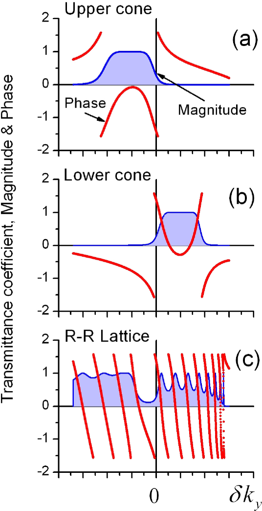
As it was mentioned in Introduction, the similarity between the energy spectra of electromagnetic waves in homogeneous media, and Dirac quasiparticles is only formal and physically meaningless, because the two cones in the photon spectra are identical. To demonstrate that the singular points (presented above) in the band gap structure of mixed periodic dielectric samples possess the properties that make them bona fide Dirac points, we considered the transmission of a monochromatic wave of a frequency through a finite stack of alternating left- and right-handed dielectric slabs. The dependencies of the amplitudes and phases on the complex transmission coefficients of the -component of the wavevector [i.e., of the angle of incidence ] are shown in Figs. 6(a) and 6(b), for two different frequencies belonging, respectively, to the upper and the lower cones in Fig. 2. While the amplitudes are similar, the phases manifest quite distinct behaviors:
| (44) |
where opposite signs correspond to two different cones, and is the position of the phase extremum. For comparison, the dependences of and for a periodic stack of normal dielectric layers are shown in Fig. 6(c). In this case, the phase is a monotonic (close to linear) function of the angle of incidence at all frequencies, and has no singularities at .
Exactly the same parabolic dependence of the phase of the transmission coefficient is intrinsic to graphene superlattices, when the contact point corresponds to the point-like transparent zone. The dependences of the amplitudes and phases of the complex transmission coefficients on the -component of the wavevector are shown in Fig. 7 for two different energies: one above [see Fig. 7(a)] and another below [see Fig. 7(b)] the energy of the zones contact.
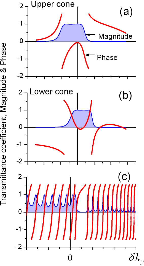
As it was mentioned above, the presence of both left- and right-handed dielectrics, or alternating and junctions in graphene, is not sufficient for a point of zone touching to be a point-like transparency zone (Dirac point). In the same lattice, points of the zone-touching with different indexes and can be either point-like gaps, as shown in Fig. 7(c), or pointlike transparent zones, i.e., Dirac points [see Figs. 7(a) and 7(b)].
A number of interesting effects emerge in the vicinity of the Dirac point of the mixed periodic sample or graphene superlattice. Some of them are caused by the parabolic dependence (44) of the transmittance coefficient phase on the angle of incidence (of ). Let us consider the propagation of a monochromatic beam of light, bounded in the transverse dimension (Gaussian beam, for instance), through the mixed stack of a thickness . Generally, a beam transmitted through a slab of a normal dielectric is shifted along the surface, as it is schematically shown in Fig. 8(a).
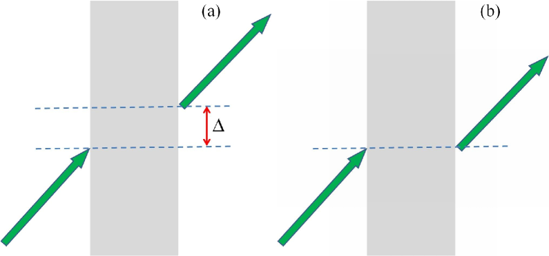
The shift is determinedArtman by evolution of the phase of the transmission coefficient :
| (45) |
where is the tangential component of the wave vector of the central ray in the incident beam. It is assumed in Eq. (45) that the angular width of the incident beam is rather small. Since mixed periodic stacks are characterized by the parabolic dependence , Eq. (44), is small or even equal to zero, in which case the longitudinal shift is absent completely.
The absence of the longitudinal shift, when , can also be observed in the so-called near-zero-index metamaterials Kocaman and in 1D periodic lattices with birefringent materials Mandatori . It is important to note that in our case, this phenomenon has a different physical origin.
The parabolic dependence affects also the curvature of the transmitted beam phase front, i.e., it shifts the focal plane of the incident Gaussian beam. The value of this shift is proportional to the thickness of the mixed stack and is independent of the stack position on the beam trajectory. The sign of the shift depends on the sign of the detuning of the beam frequency from the Dirac-point frequency . The focal plane is shifted forward (defocusing) when , and backward (focusing) when .
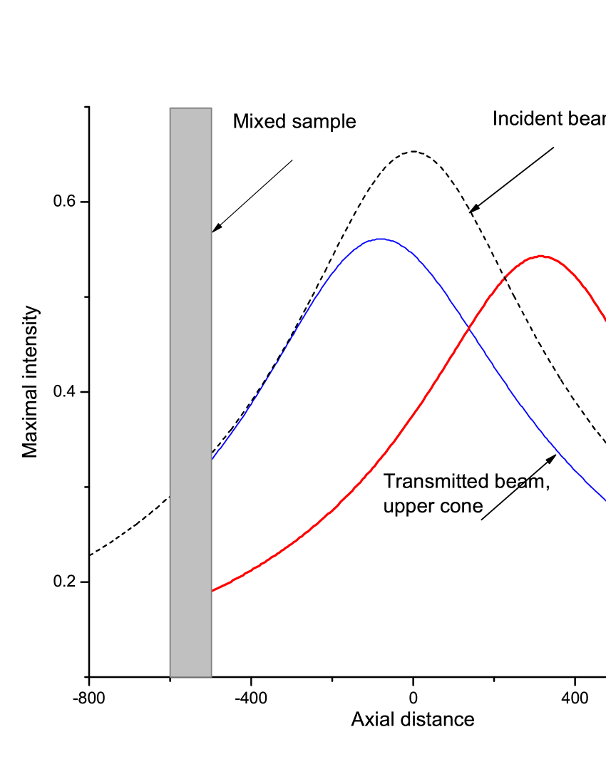
This surprising focusing properties of mixed periodic samples are demonstrated in Fig. 9. Of the two beams with the frequencies resting on two different dispersive cones, the one corresponding to the upper cone is focused by the sample, blue curve, while the other (lower cone) is defocused, red line. For comparison, the black curve presents the intensity distribution in the beam propagated in free space. This phenomenon is highly unusual by itself, and also reinforces the similarity of the contact points of the cones to a genuine “optical” Dirac point: different cones are not identical, and represent objects with distinct physical properties — a sort of optical particle-antiparticle pair.
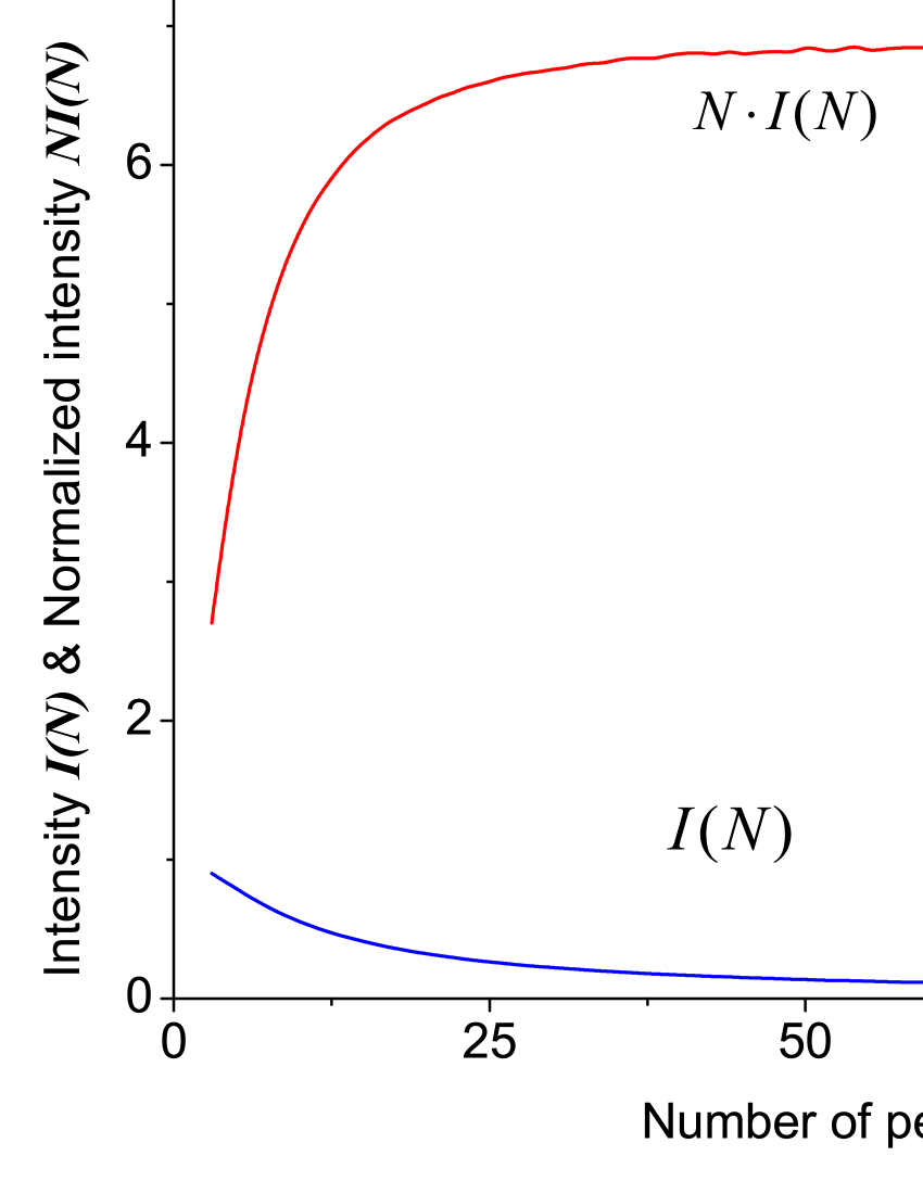
When the frequency of the incident beam coincides with a point-like gap of the corresponding infinite structure, i.e., , one would expect an exponential decay of the transmitted beam intensity as a function of the mixed stack thickness : . However, the well-pronounced constant asymptotic of the function (Fig. 10, red line), demonstrates an anomalously high intensity, decaying as . Such a diffusion-like dependence is one of the consequences of the linear, Dirac cone-like dispersion. In two-dimensional photonic crystals with triangular lattices of normal dielectric rods, this phenomenon was predicted in Ref. 9, . In layered structures, it could take place only in the presence of left-handed elements.
Because of the similarity between the energy spectrum of relativistic electrons and the frequency band structure of a mixed periodic dielectric structure, it is natural to assume that the light beam propagation into mixed samples can be accompanied by a Zitterbewegung-like phenomenon. Indeed, the spatial distribution of the energy flux inside the mixed sample manifests a trembling motion: the “center of gravity” of the flux oscillates in the transverse direction (along the -axis). In Fig. 11, the spatial distribution of the energy flux inside the mixed sample is shown. The oscillatory motion of the center of gravity is clearly seen in Fig. 12. Note that Fig. 11 is similar to Fig. 3 in Ref. Thaler, , where the probability function of a moving electron (solution of the Dirac equation) is shown.
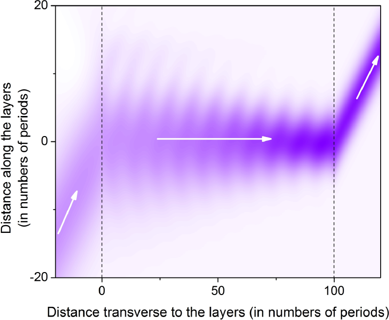

Figure 11 also demonstrates the two above-mentioned effects: the absence of the longitudinal shift (the energy propagates normally to the sample boundary, whereas the angle of incidence of the beam is far from the normal) and the focusing of the beam.
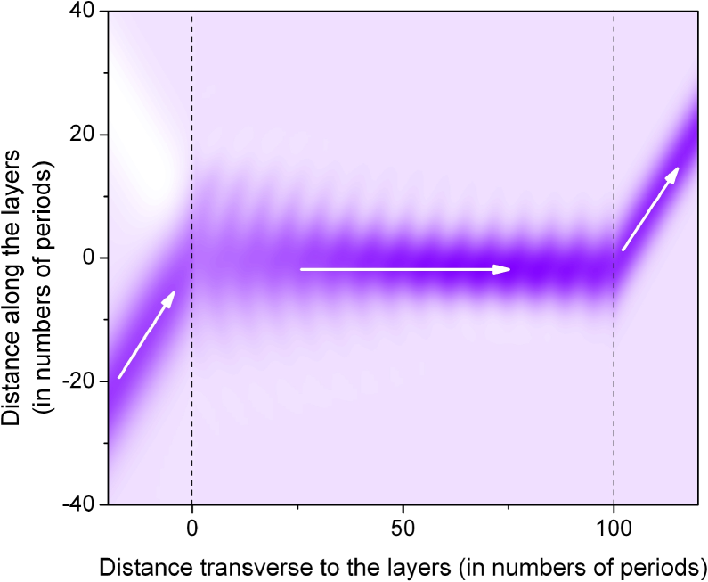
All these effects — the absence of the longitudinal shift, the focusing of the beam, and the Zitterbewegung phenomenon — are also seen in graphene superlattices. As an example, the current density distribution in the Gaussian beam of monoenergetic charge carriers propagating through a finite graphene superlattice is depicted in Fig. 13.
Let us now compare the wave propagation through a mixed dielectric slab or a graphene superlattice with the transmission of an electromagnetic wave through a plate made of a homogeneous (right- or left-handed) dielectric. In a small vicinity of the normal angle of incidence, the dependence of the transmission coefficient phase on the tangential component of the wave number (the dependence on the angle of incidence) has the same parabolic form as discussed above [see Eq. (44)], with the only difference that at homogeneous dielectric plates, by definition:
| (46) |
Here the plus sign corresponds to right-handed dielectrics, while the minus sign corresponds to left-handed dielectrics. In the first case, the refraction is positive, i.e., the incident beam and the beam inside the plate lie on opposite sides from the normal; whereas in the second case, the beams lie on the same side of the normal (negative refraction). Therefore, the shift is positive for plates of a right-handed dielectric, and negative for left-handed dielectrics. In other words, in normal samples, and have the same signs, while in metamaterials the signs are opposite. Amazingly, these two situations, each inherent to different kinds of homogeneous materials, can be observed in the same mixed periodically-layered sample, and graphene superlattice. Indeed, depending on which side of the Dirac point the frequency lies, the refraction is either positive (upper cone), or negative (lower cone). In this regard, it is more appropriate to refer to these two cones as a “medium – anti-medium” pair, rather than “particle–antiparticle”, as in homogeneous graphene.
VI Conclusions
We have shown that some of the exotic properties of charge transport in graphene can be reproduced in the propagation of light through layered dielectric samples. Similarities and distinctions between Maxwell and Dirac equations, and between the corresponding boundary conditions have been studied. Although the equations for the real electric and magnetic fields are essentially different from those for the Dirac electrons, under some conditions they can be reduced to similar form. For example, Eq. (II) for the complex combinations given by Eq. (3) coincides with the Dirac equations (II). Therewith, the role of the refractive index in graphene is played by the difference between properly normalized values of the Fermi energy and the external electrostatic potential [Eq. (II)]. The boundary conditions for a Dirac quasiparticle incident on a plane separating two areas with different potentials, and for an electromagnetic wave propagating through an interface between two layers of homogeneous dielectrics are, generally speaking, different. They coincide only when the impedances of the layers are equal, and the direction of the propagation is normal to the boundary. It means that at normal incidence, any junction in graphene is analogous to a contact between two perfectly matched dielectrics and therefore is absolutely transparent to normally-incident Dirac electrons. This provides a more intuitive insight into the physics of the Klein paradox in graphene.
The analytical and numerical analysis of the photonic band gap structures of infinite periodically-layered systems reveals an infinite number of the so-called “diabolic points” (singular points of contact of two transparency zones) in the spectral diagrams (examples are shown in Fig. 4). A distinction needs to be drawn between two types of these singularities: point-like transparency zones, like in Figs. 4(a) and 4(c), and pointlike gaps in the spectrum, similar to the one presented in Fig. 4(c). Although all three pictures in Fig. 4 are topologically equivalent, the transport properties of the corresponding finite periodic stacks of layers differ drastically in the vicinities of these points. Waves with frequencies lying on opposite sides of the singularities of the first type propagate through the samples in similar ways. In the same time, when two touching spectral cones form a point-like gap, the electromagnetic radiation interacts with the same sample differently, depending to which cone its frequency belongs. Studies of the propagation of beams of light show that only the diabolic points of this type posses the properties of genuine Dirac points. We demonstrate that in mono-type layered structures (i.e., in those built of either normal or left-handed dielectrics) just the diabolic point of the first type can exist, and conical, Dirac-type singularities appear only in mixed (with alternating left- and right-handed layers) samples. This is in contrast to two-dimensional media where Dirac points were discovered in various types of photonic crystals with normal dielectric elements. It is important to note that the physical nature of the Dirac points that we consider is different from that in systems with zero average value of the refractive index: in mixed layered structures, they are due to the specific strong dispersion (phase and group velocities have different signs) inherent in the elements with negative refraction.
Although the angular dependencies of the transmission and reflection coefficients from a single interface in layered dielectrics and graphene superlatices are different [compare formulas Eqs. (III) and (III)], the spectral properties of these two structures are conceptually identical and entail similar features in the light and charge transport. Considering, as examples, the transmission of the Gaussian monochromatic beams of light and monoenergetic Dirac electrons through the corresponding (dielectric or graphene) samples we predict the following Dirac-point-induced effects: (i) two touching Dirac cones influence the propagation of a beam in different ways: the beam is focused when the frequency (energy) belongs to the upper cone, and is defocused at frequencies (energies) lying in the lower one, (ii) the transverse shift of the beam is anomalously small or even zero, (iii) the decay of the intensity at forbidden frequencies is diffusion-like, and (iv) a spatial analog of the Zitterbewegung effect (i.e., trembling motion of the “center of gravity” of the energy flux) is observed in periodically layered dielectric structures with nonzero average refractive indices and in graphene superlatices.
VII Acknowledgments
This work was supported in part by JSPS-RFBR Grant No. 12-02-92100, RFBR Grant No. 11-02-00708, ARO, RIKEN iTHES Project, MURI Center for Dynamic Magneto-Optics, Grant-in-Aid for Scientific Research (S), MEXT Kakenhi on Quantum Cybernetics, the JSPS via its FIRST program, and by the Israeli Science Foundation (Grant No. 894/10).
*
Appendix A Boundaries of the transparency zones of photonic structures
Boundaries of the transparency zones in the plane in the vicinity of the zones touching point are defined by the equation
| (47) |
where are defined by Eqs. (40). It follows from Eq. (47), that
| (48) |
where
This equation, using Eq. (40), can be presented in the form:
| (49) |
When the photonic structure is formed by either right- or left-handed layers only, i.e., and , both lines lie in the same quadrants and the zones touching point forms a point-like gap, as it is shown, for instance, in Fig. 4a. In the mixed structure which contains both left- and right-handed layers, i.e., and , the situation is quite different. The denominator in Eq. (49) has the same sign for both and , while the signs of the numerator can be different. Whether the sign of is equal to or depends on the values of the parameters. The zones structures in the first [] and the second [] cases are similar to ones shown in Fig. 4b and Fig. 4c, respectively.
Thus, the zones touching point presents the point-like transparent zone when the following inequalities hold:
| (50) |
Using the definition of the parameter and Eq. (IV) these inequalities can be written as
| (51) |
when
and reverse to Eq. (51) inequalities, when
As it follows from Eq. (IV), the range of allowed values of the parameters is restricted by the condition
| (52) |
when , and by the reverse inequality when .
All these inequalities select a region in the 4-dimensional space of parameters , , , and , where the vicinity of the zones contact point is characterized by the Dirac-like spectrum.
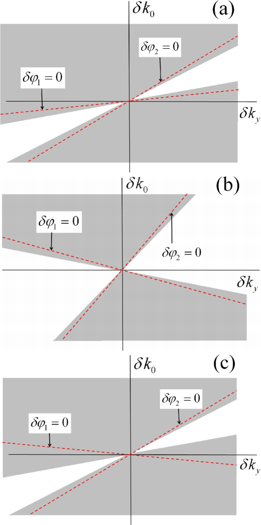
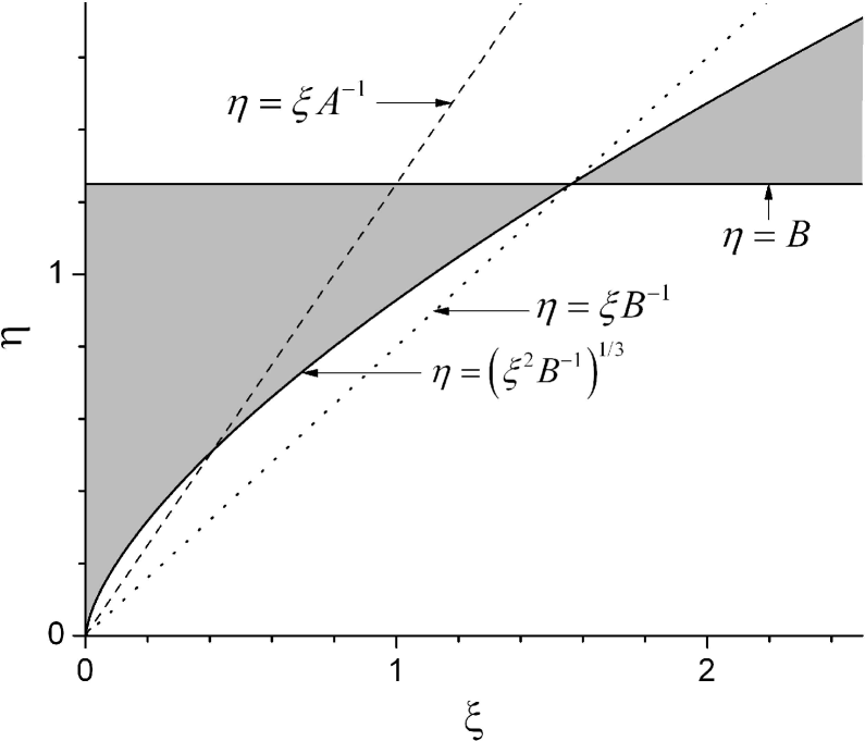
Any metamaterial-dielectric pair is characterized by its own values of the parameters and . Therefore, considering these parameters as given, one can define the corresponding area in the two-dimensional space of parameters and (remainder: and are integer numbers). Introducing the notations and we can write the inequalities Eqs. (51) and (52) as
| (53) |
and
| (54) |
Equation (A) means that the line divides the plane in two parts. The allowed values of variables and lie below this line if , and above the line if . Inequalities Eq. (A) bound an area between the line and the curve . The region where a touching point of the zones presents the genuine Dirac point is defined by the intersection of these two areas, as it is shown in Fig. 14.
Note, that the group velocities and are not involved in this analysis. These velocities define the angle of opening of the Dirac spectrum, but not the fact of its existence.
Usually, metamaterials exhibit their left-handed properties in a rather narrow frequency range. Because the above-mentioned region is defined only by the relation between the layer thicknesses and , one can tune the Dirac point frequency by an appropriate choice of the structure period .
References
- (1) V.G. Veselago, Sov. Phys. Usp. 10, 509 (1968).
- (2) P.R. Wallace, Phys. Rev. B 71, 622 (1947).
- (3) I. Bialynicki-Birula, Progress in Optics, XXXVI (1996).
- (4) I. Bialynicki-Birula, Z. Bialynicka-Birula, J. Phys. A: Math. Theor. 46, 053001 (2013); arXiv: 1211.2655 (2012).
- (5) F.D.M. Haldane, S. Raghu, Phys. Rev. Lett. 100, 013904 (2008).
- (6) L.-G. Wang, Z.-G. Wang, J.-X. Zhang, S.-Y. Zhu, Opt. Lett. 34, 1510 (2009).
- (7) T. Ochiai, M. Onoda, Phys. Rev. B. 80, 155103 (2009).
- (8) K.Y. Bliokh, A.Y. Bekshaev, and F. Nori, New J. Phys. 15, 033026 (2013).
- (9) A.V. Shytov, M.S. Rudner, and L.S. Levitov, Phys. Rev. Lett. 101, 156804 (2008).
- (10) J.L. Garcia-Pomar, A. Cortijo, M. Nieto-Vesperinas, Phys. Rev. Lett. 100, 236801 (2008).
- (11) P. Darancet, V. Olevano, and D. Mayou, Phys. Rev. Lett. 102, 136803 (2009).
- (12) A.V. Rozhkov, G. Giavaras, Y.P. Bliokh, V. Freilikher, F. Nori, Phys. Rep. 503, 77 (2011).
- (13) X. Chen, P.-L.Zhao, X.-J. Lu, arXiv:1111.1753 (2011); X. Chen, X.-J. Lu, Y. Ban, and C.-F. Li, J. Optics 15, 033001 (2013).
- (14) Y.P. Bliokh, V. Freilikher, S. Savel’ev, F. Nori, Phys. Rev. B 79, 075123 (2009).
- (15) R. Polles, A. Moreau, G. Granet, Opt. Let. 35, 3237 (2010).
- (16) H. Benisty, N. Piskunov, P. Kashkarov, O. Khayam, Phys. Rev. A 84, 063825 (2011).
- (17) H. Benisty, O. Khayam, IEEE J. Quant. Electronics 47, 204 (2011).
- (18) H. Benisty, Phys. Rev. B 79, 155409 (2009).
- (19) R. Sepkhanov, Ya. Bazaliy, C. W. J. Beenakker, Phys. Rev. A 75, 063813 (2007).
- (20) M. Plihal, A. Shambrook, A. A. Maradudin, Opt. Commun. 80, 199 (1991).
- (21) M. Plihal, A.A. Maradudin, Phys. Rev. B 44, 8565 (1991).
- (22) D. Cassagne, C. Jouanin, D. Bertho, Phys. Rev. B 52, R2217 (1995); 53, 7134 (1996); Appl. Phys. Lett. 70, 289 (1997).
- (23) F. Gadot, A. Chelnokov, A.D. Lustrac, P. Crozat, J.-M. Lourtioz, D. Cassagne, C. Jouanin, Appl. Phys. Lett. 71, 1780 (1997).
- (24) L. Martinez, A. Garcia-Martin, P. Postigo, Opt. Express 12, 5684 (2004).
- (25) K. Busch, G. von Freymann, S. Linden, S. Mingaleev, L. Tkeshelashvili, M. Wegener, Phys. Reports 444, 101 (2007).
- (26) F.D.M. Haldane, S. Raghu, Phys. Rev. A 78, 033834 (2008).
- (27) M. Diem, T. Koschny, C.M. Soukoulis, Physica B 405, 2990 (2010).
- (28) X. Zhang, Phys. Rev. Let 100, 113903 (2008).
- (29) Q. Liang, Y. Yan, J. Dong, Opt. Lett. 36, 2513 (2011) .
- (30) F. Dreisow, M. Heinrich, R. Keil, A. Tünnermann, S. Nolte, S. Longhi, A. Szameit, Phys. Rev. Let. 105, 143902 (2010).
- (31) T. Ando, T. Nakanishi, and R. Saito, J. Phys. Soc. Japan 67, 2857 (1998).
- (32) K.Y. Bliokh, Phys. Lett. A, 344, 127 (2005).
- (33) R. Sepkhanov, A. Ossipov, C. W. J. Beenakker, Eur. Phys. Lett. 85, 14005 (2009).
- (34) O. Peleg, G. Bartal, B. Freedman, O. Manela, M. Segev, D. N. Christodoulides, Phys. Rev. Lett. 98, 103901 (2007).
- (35) M. Rechtsman, Y. Plotnik, D. Song, M. Heinrich, J. M. Zeuner, S. Nolte, N. Malkova, J. Xu, A. Szameit, Z. Chen, M. Segev, arXiv:1210.5361 (2012).
- (36) M.C. Rechtsman, Y. Plotnik, J.M. Zeuner, A. Szameit, M. Segev, arXiv:1211.5683 (2012).
- (37) X. Huang, Y. Lai, Z. H.Hang, H. Zheng, C. T. Chan, Nat. Mater. 10, 582 (2011).
- (38) K. Sakoda and H-F. Zhou, Opt. Express 18, 27371 (2010); 19, 13899 (2011); K. Sakoda, Opt. Express 20, 3898 (2012); 20, 9925 (2012); 20 25181, (2012); J. Opt. Soc. Am. B 29, 2770 (2012).
- (39) S. Matsuzawa, K. Sato, Y. Inoue, T. Nomura, IEICE Trans. Electron. E89-C, 1337 (2006).
- (40) I. Nefedov, S. Tretyakov, Phys. Rev. E 66, 036611 (2002).
- (41) L. Wu, S. He, L. Shen, Phys. Rev. B 67, 235103 (2003).
- (42) D. Bria, B. Djafari-Rouhani, A. Akjouj, L. Dobrzynski, J. Vigneron, E. El Boudouti, A. Nougaoui, Phys. Rev. E 69, 066613 (2004).
- (43) M. Tashima and N. Hatano, arXiv:1306.0297 (2013).
- (44) M. Katsnelson, K. S. Novoselov, A. Geim, Nat. Phys. 2, 620 (2006).
- (45) V. Cheianov, V. Fal’ko, B. Altshuler, Science 315, 1252 (2007).
- (46) J. B. Pendry, Phys. Rev. Lett. 85, 3966 (2000).
- (47) A. Young, P. Kim, Nat. Phys. 5, 222 (2009).
- (48) Y.P. Bliokh, V. Freilikher, F. Nori, Phys. Rev. B 81, 075410 (2010).
- (49) P.E. Allain and J.N. Fuchs, Eur. Phys. J. B 83, 301 (2011).
- (50) P. Yeh, A. Yariv, .C.-S. Hong, J. Opt. Soc. Am. 97, 423 (1977).
- (51) M.V. Berry and M.R. Jeffrey, Progress in Optics 50, 13 (2007).
- (52) J. Li, L. Zhou, C.T. Chan, P. Sheng, Phys. Rev. Lett. 90, 083901 (2003).
- (53) X. Huang, Y. Lai, Z. H. Hang, H. Zheng, C. T. Chan, Nature Mat. 10, 582 (2011).
- (54) K. Artmann, Ann. Phys. Lpz. 2, 87 (1948).
- (55) M.G. Silveirinha, N. Engheta, Phys. Rev. Lett. 97, 157403 (2006).
- (56) N.C. Panoiu, R.M. Osgood, Jr., S. Zhang, and S.R.J. Brueck, J. Opt. Soc. Am. B 23, 507 (2006).
- (57) S. Feng, Phys. Rev. Lett. 108, 193904 (2012).
- (58) S. Kocaman, M.S. Aras, P. Hsieh, J.F. McMillan, C.G. Biris, N.C. Panoiu, M.B. Yu, D.L. Kwong, A Stein, and W. Wong, Nat. Photonics 5, 499 (2011).
- (59) A. Mandatori, C Sibilia, M. Bertolotti, S. Zhukovsky, J.W. Haus, and M. Scalora, Phys. Rev. B 70, 165107 (2004).
- (60) B. Thaller, arXiv:quant-ph/0409079 (2004).