∎
Multiple Andreev reflections spectroscopy of two-gap 1111- and 11 Fe-based superconductors
Abstract
Using the “break-junction” technique we prepared and studied superconductor - constriction - superconductor nanocontacts in polycrystalline samples of Fe-based superconductors CeO0.88F0.12FeAs (Ce-1111; K), LaO0.9F0.1FeAs (La-1111; K), and FeSe ( K). We detected two subharmonic gap structures related with multiple Andreev reflections, indicating the presence of two superconducting gaps with the BCS-ratios and , respectively. Temperature dependences of the two gaps in FeSe indicate a -space proximity effect between two superconducting condensates. For the studied iron-based superconductors we found a linear relation between the gap and magnetic resonance energy, .
Keywords:
Fe-based superconductors two-gap superconductivity multiple Andreev reflections subharmonic gap structure “break-junction”pacs:
74.70.Xa 74.25.-q 74.45.+c1 Introduction
Andreev spectroscopy Andreev is a powerful instrument to measure superconducting gap in a wide temperature range, up to Kummel ; Poenicke ; Blonder . A number of such measurements have been performed earlier with oxypnictides of the RFeAsO1-xFx family and with FeSe Seidel ; LOFA ; Gd ; FeSe . Here we present systematic studies of the current-voltage characteristics (CVCs) and dynamic conductance for superconductor - constriction - superconductor (ScS) contacts in Ce-1111, La-1111 and FeSe. Using the intrinsic multiple Andreev reflections effect (IMARE) spectroscopy, we measured the two superconducting gap values in all three Fe-based materials and determined temperature dependences of the two gaps for FeSe.
The compounds under study belong to the class of iron-based superconductors discovered in 2008 Kamihara . These materials are characterized by a layered crystal structure; their electron energy spectrum in the normal state contains electron and hole quasi-two-dimensional Fermi surface sheets, where two superconducting condensates are supposed to be formed at Seidel .
2 Experimental details
To measure the superconducting gaps we used two methods: (i) Andreev spectroscopy Andreev of single ScS nanocontacts Kummel , and (ii) IMARE spectroscopy of ScS-contact stacks. The nano-sized contacts required for multiple Andreev reflections spectroscopy, have been made using the “break-junction” technique Moreland . In this technique, breaking a bulk sample in the cryogenic environment creates a superconductor - constriction - superconductor (ScS) junctions. Bias current flowing through the sub-mcm size constriction exceeds the superconducting critical current value and causes the contact area transition to the normal state; as a result, the studied ScS-contacts may be considered as conventional SnS-junctions.
The main features of the curves for our ScS-contacts comprise a pronounced excess current at low bias voltages and a subharmonic gap structure (SGS) in the curve. The latter shows sharp dips at a set of bias voltages . For interpreting these dips we use theoretical model by Kümmel et al. Kummel , applicable for conductance spectra of the symmetric ScS-contacts:
| (1) |
As the subharmonic number increases, the dip amplitude decays. By plotting the dependence (which must pass through the point) it is easy to determine the gap value accurately. In the case of a two-band superconductor, two distinct SGS should be observed.
Due to the local character of the Andreev spectroscopy of ScS break junctions, studies of the SGS for individual Sharvin type Sharvin nanocontacts allow to gain information even in case of inhomogeneous samples. In order to observe SGS, the size of the Andreev contact should be significantly smaller than the quasiparticles mean free path (the ballistic regime) Kummel ; Poenicke ; Blonder .
Because of the layered structure of Fe-based superconductors, exfoliation of the sample generates nanosteps and terraces in the -direction and thus may form not only single ScS-junctions but also arrays of the S-c-S-c-…-S- type junctions. The array represents a stack of several consequently connected ballistic ScS-junctions causing an intrinsic multiple Andreev reflections effect. The latter is similar to the intrinsic Josephson effect in SIS-array Nakamura . Using stacks of contacts, one can exclude surface distortion of superconductivity and observe sharp peculiarities corresponding to the true bulk gaps. Bias voltages for these singularities should scale with the number of contacts in the stack.
For temperatures up to , the gap may be obtained directly by substituting to Eq.(1) the bias voltages corresponding to the dips Kummel . Our data for three different materials are shown in Figs. 1-5; they are typical for clean classical SnS-contacts Kummel . As will be shown below, the data manifest two distinct sequences of dips.
The and dI(V)/dV-characteristics were measured by a computer controlled set-up using a 16 bit National Instrument board. The dynamic conductance spectra were measured by a standard modulation technique Rakhmanina .
3 Experimental results
3.1 CeO1-xFxFeAs
In this section we present Andreev spectroscopy data for Ce-1111 break junctions. The results reveal the existence of two superconducting energy gaps and enable evaluating their magnitude at K. To the best of our knowledge, the gap values were not measured for this material earlier. The polycrystalline CeO0.88F0.12FeAs samples with were synthesized as described in Khlybov .
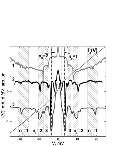
Dynamic conductance for three single ScS-contacts , (marked as 1 and 2) for sample Ce1, and (3) for sample Ce2 is shown in Fig. 1, where one can see two sets of SGS. For comparison, the figure also shows the excess-current CVC for contact (3). The dashed areas comprise respective minima of the first set (marked with labels and originating from the large gap) and represent a 15% uncertainty. Somewhat reduced intensity of the minima may be caused by a slight overheating of the contact area at the highest bias voltages. The fine structure in the bias voltage interval between and signals a large gap anisotropy of about 30%.
The small gap SGS starts with minima located at mV (marked with dash-dotted vertical lines and labels) which have rather high relative amplitude, higher than the third Andreev dip from the large gap SGS. The sharp increase in the dip amplitude signals onset of a new SGS. Beyond the dips one can also see the dips located at mV.
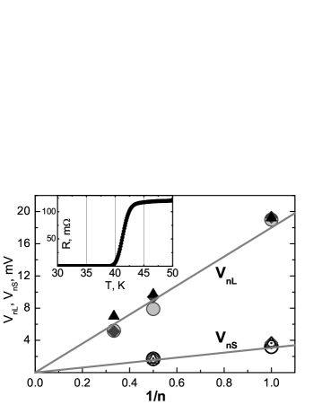
The Andreev minima positions for the large and the small gap are plotted in Fig. 2 as a function of . The plot clearly demonstrates the anticipated linear dependence which proves unambiguously that the dips in Fig. 1 do form two independent SGS, related with the presence of two superconducting gaps. The slope of the two fitting lines gives meV, and meV, for the large and small gaps, respectively. Taking into consideration the bulk K values (see inset to Fig. 2), we find the BCS ratio for the large gap, and for the small gap.
3.2 LaO1-xFxFeAs
We studied about 50 ScS-Andreev contacts in polycrystalline LaO0.9F0.1FeAs (LOFA) samples with bulk = K. The dynamic conductance of single contacts and nanosteps demonstrates two well-reproducible sets of SGS corresponding to the pair of independent gap values. The number of elementary contacts in a stack was controlled by comparing the single contact spectra with those for several stacks normalized to a single junction spectrum. Figure 3 shows the spectra for a single contact (black curve) and for the stacks and with various number of junctions in the array (, gray curve dI9(V)/dV, and , dashed curve dI10(V)/dV, respectively). Scaling of the SGS with properly selected number of contacts in nanosteps is straightforward. Following the equation of Kümmel et al. Kummel , we easily obtain the large gap meV. As for the small gap minima, peculiarities marked by arrows (at the top of Fig. 3 and in the inset) give meV and 1.25 meV values at K for the single contact and for the array , respectively. By tracing the temperature dependence, we found the local critical temperature of the contact area . The values obtained, meV, meV, and K are close to the results of Yashima .
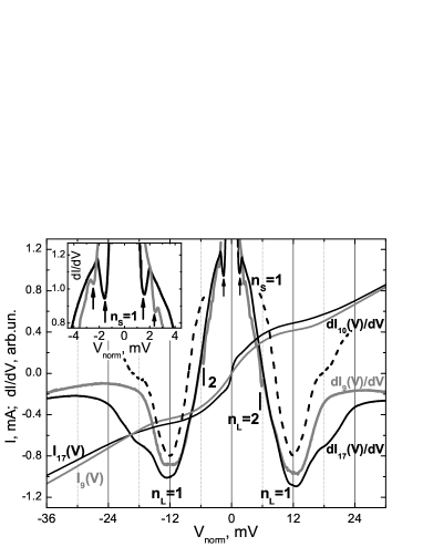
Figure 4 shows normalized CVC and dynamic conductance of two-contact ScS-Andreev array in another LaO(F)FeAs sample. The sharp SGS related to the large gap (marked with labels) gives meV (see solid squares in the inset to Fig. 4). Interestingly, all these Andreev minima up to are double-splitted. It seems that the doublets observed on the high-quality characteristics are caused by some anisotropy of the order parameter, though it has no nodes, as was shown in LOFA . The CVC shown in Fig. 4 demonstrates a small Josephson supercurrent at zero bias caused by the tunneling between the sample clefts. An SGS associated with the small gap ( labels and arrows) leads to meV value (see open squares in the inset to Fig. 4).
The BCS-ratio exceeds the standard value 3.52 and thus is in favor of a strong coupling in the condensate. At the same time, the small value, , is a result of induced superconductivity at finite temperatures in the bands with the small gap. These values support data reported earlier in LOFA and are in close agreement with the experimental results on GdO(F)FeAs Gd and our data on MgB2 SSC ; MgB2 .
3.3 FeSe
Among the new class of Fe-based superconductors Kamihara , layered FeSe has the simplest crystal structure and relatively low critical temperature . Polycrystalline FeSe samples have been grown from melt by spontaneous nucleation. The synthesis process was described in detail in FeSe . The intrinsic multiple Andreev reflections effect was observed in FeSe nanosteps earlier FeSe .
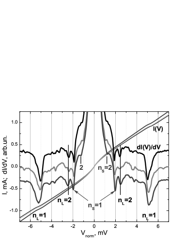
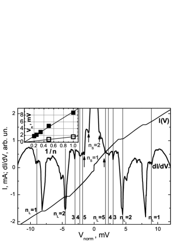
The and characteristics for several ScS-junctions formed by successive mechanical readjustments of the contact are shown in Fig. 5. Two sets of SGS with a number of dips are clearly seen. The first set of dips ( labels) gives the large gap value meV. The second set of dips ( labels) corresponds to the small gap meV. It is worth noting that the dip positions and, consequently, the gap values remain unchanged under the readjustment of the contact. This proves the high homogeneity of the sample superconducting properties in the contact area. The superconducting gap values at K averaged over more than 30 ScS-contacts, are meV and meV ( K). These results agree with the preliminary data obtained with similar samples FeSe .
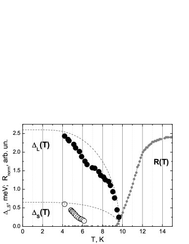
Figure 6 shows the temperature dependences for two ScS-contacts in FeSe. For the large gap, the -curve lies slightly below the standard BCS-like dependence. For the small gap, the dependence deviates essentially from the BCS-type curve and is in a good agreement with the calculations in Khasanov . Knowing the local K, one can calculate the BCS-ratio. For the large gap, we obtain which exceeds the BCS value for a single-gap superconductor. On the other hand, for the small gap, the ratio is much smaller than 3.52. Such a behavior resembles the situation in MgB2 MgB2 ; SSC12 ; Nicol and, by parity of reasoning, can be explained by the -space proximity effect Golubov ; Yanson between two superconducting condensates, where the large gap condensate plays a “driving” role.
4 Discussion
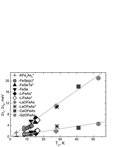
It was pointed out Onari that inelastic neutron scattering data can provide a valuable information about the symmetry of the superconducting gap in novel superconductors. Calculations showed, in particular, that a hump structure must appear in the dynamic spin susceptibility just above the energy in the case of an wave state (the fully gapped -wave state without sign reversal) Onari . Recently, the experimental linear dependence of the spin resonance energy on with the average slope was found for several iron based superconductors (see, e.g. Fig. 5 in Shamoto ). Within experimental errors, this dependence coincides with our plot (Fig. 7) of the superconducting gap versus for several iron based superconductors: Ce-1111 (present measurements), FeSe (FeSe ), LaO(F)FeAs LOFA , GdO(F)FeAs Gd , as well as KFe2As2, FeTe1-xSex, LiFeAs, (see Fig. 11 in FeSe and Refs. therein). Although the scattering of data in Fig. 7 is quite significant, two linear dependences emerge with and . The coincidence of (Fig. 7) and (Fig. 5 in Shamoto ) supports the version of a fully gapped -wave state without sign reversal Onari .
In conclusion, we studied properties of CeO(F)FeAs, LaO(F)FeAs, and FeSe superconductors by ScS-Andreev- and IMARE spectroscopies. The dynamic conductance curves for single and stack ScS-contacts cannot be described within the single-gap framework and evidence for the two-gap superconductivity in these compounds. For the first time studied CeO(F)FeAs ( K) we determined the two superconducting gaps meV, and meV; the respective BCS-ratios are , and .
For LaO(F)FeAs ( K) we also determined the two superconducting gap values meV, meV, leading to the BCS-ratios and , respectively ( K). We observed splitting of the SGS dips for high-quality characteristics, suggestive of an anisotropy of the order parameter.
For FeSe ( K) our IMARE spectroscopy data point to meV, meV, and , . The temperature dependences indicate the -space proximity effect between two superconducting condensates. The large gap BCS-ratio for all the materials studied exceeds 3.52, indicating a strong electron-boson coupling in the “driving” large gap condensate. The BCS-ratio for the small gap appears to be much less than 3.52, thus suggesting an induced superconductivity at finite temperatures in the “driven” condensate due to a nonzero interband coupling. Finally, our data confirm a linear relation between the superconducting gap and magnetic resonance energy , valid for various Fe-based superconductors.
Acknowledgements.
The work was supported by Russian Ministry of Education and Sciences (contract 11.519.11.60.12, grant 8375), RFBR (grants 12-02-31269, 13-02-01451), DFG Grants 436RUS113 and FOR 538/BU887/4, and DFG priority program (SPP1458). We thank T. Hänke, C. Hess, G. Behr, R. Klingeler and B. Büchner for the La-1111 samples synthesis.References
- (1) A.F. Andreev, Sov. Phys. JETP 19, 1228 (1964).
- (2) R. Kümmel et al., Phys. Rev. B 42, 3992 (1990).
- (3) A. Poenicke et al., Phys. Rev. B 65, 220510 (2002).
- (4) G.E. Blonder et al., Phys. Rev. B 25, 4515 (1982).
- (5) P. Seidel, Supercond. Sci. Technol. 24, 043001 (2011).
- (6) Ya.G. Ponomarev, et al., Phys. Rev. B 79, 224517 (2009).
- (7) T.E. Shanygina et al., JETP Lett. 93, 94 (2011).
- (8) Ya.G. Ponomarev et al., J. Exp. Theor. Phys. 113, 459 (2011).
- (9) Y. Kamihara et al., J. Am. Chem. Soc. 130, 3296 (2008).
- (10) J. Moreland, J. W. Ekin, J. Appl. Phys. 58, 3888 (1985).
- (11) Yu.V. Sharvin, Zh. Eksp. Teor. Fiz. 48, 984 (1965).
- (12) H. Nakamura et al., J. Phys. Soc. Jpn. 78, 123712 (2009).
- (13) Ya.G. Ponomarev, A. V. Rakhmanina, Prib. Tehn. Eksp. 5, 120 (1970).
- (14) E.P. Khlybov et al., JETP Lett. 90 (2009).
- (15) M. Yashima, et al., J. Phys. Soc. Jpn. 78, 103702 (2009).
- (16) Ya.G. Ponomarev et al., Solid St. Comm. 129, 85 (2004).
- (17) R. Khasanov et al., Phys. Rev. Lett. 104, 087004 (2010).
- (18) Ya.G. Ponomarev et al., JETP Lett. 79, 484 (2004).
- (19) S.A. Kuzmichev et al., Solid St. Comm. 152, 119 (2012).
- (20) E.J. Nicol, J. P. Carbotte, Phys. Rev. B 71, 054501 (2005).
- (21) A.A. Golubov et al., Phys. Rev. B 51, 1073 (1995).
- (22) I.K. Yanson et al., Phys. Rev. B 67, 024517 (2003).
- (23) S. Onari et al., Phys. Rev. B, 81, 060504 (2010).
- (24) Shin-ichi Shamoto et al., Phys. Rev. B 82, 172508 (2010).